Page 1

PHOTODARLINGTON OPTICAL
INTERRUPTER SWITCH
QCK3 QCK4
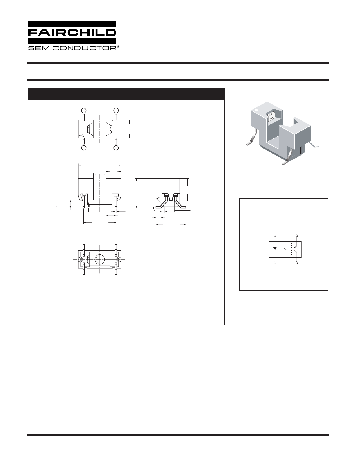
PACKAGE DIMENSIONS
2
C
L
PIN 1
IDENTIFICATIO
N
1
0.527
0.157
OPTICAL C OPTICAL C
L
0.005
0.295±
0.005
0.100±
OPTICAL C
0.015
0.400±
L
C
L
C
L
C
L
0.020
0.185
3
4
0.1215
00
0.22
0.020SQ
(4X)
C
L
PIN 1 CATHODE
PIN 2 ANODE
PIN 3 EMITTER
PIN 4 COLLECTOR
0.020
(4X)
0.365±
0.0283
45.0°
(2X)
L
C
L
0.060±0.020
(4X)
0.020
0.370±
0.280
0.085
(4X)
SCHEMATIC
2
1
3
4
NOTES:
1. Dimensions for all drawings are in inches.
2. Tolerance of ± .010 on all non-nominal dimensions
unless otherwise specified.
3. All leads are coplanar within .006".
4. Housing material is electrically conductive.
DESCRIPTION
The QCK3/QCK4 is a slotted opticalswitch designed for surface mount applications where extreme temperatures are experienced
during solder reflow. The switch consists of a GaAs LED and a silicon photodarlington facing each other across a.157" (4.0 mm)
gap. The leads are formed to sit flush on a PCB during solder reflow.
FEATURES
• Unique single piece housing designed to reduce cost.
• High temperature housing material to withstand extreme temperature.
• Shipped in plastic tubes for protection of leads and to feed automatic placement equipment.
• Sensor package is infrared transparent and tinted to attenuate visible light.
© 2002 Fairchild Semiconductor Corporation
Page 1 of 3
5/13/02
Page 2

PHOTODARLINGTON OPTICAL
INTERRUPTER SWITCH
QCK3 QCK4
ABSOLUTE MAXIMUM RATINGS
(T
= 25°C unless otherwise specified)
A
Parameter Symbol Rating Units
T
T
T
SOL-F
OPR
STG
-55 to +100 °C
-40 to +85 °C
Operating Temperature
Storage Temperature
Soldering Temperature (Flow)
Preheating Stage for 60 sec 183 °C
Reflow Stage for 5 sec 230 °C
Rate of Temperature Rise 3 to 10 °C/S
EMITTER
Continuous Forward Current
Reverse Voltage
Power Dissipation
(1)
I
F
V
R
P
D
50 mA
6 V
100 mW
SENSOR
V
V
CEO
ECO
I
C
P
D
30 V
6 V
40 mA
150 mW
Collector-Emitter Voltage
Emitter-Collector Voltage
Collector Current
Power Dissipation
(1)
NOTE:
1. Derate power dissipation linearly 1.33 mW/°C above 25°C.
PARAMETER DEVICES TEST CONDITIONS SYMBOL MIN TYP MAX UNITS
EMITTER
Forward Voltage
Reverse Current
= 20 mA V
F
V
= 2 V I
R
F
R
——1.4 V
——100 µA
I
SENSOR
Collector-Emitter Breakdown
Collector-Emitter Leakage
= 1 mA, E
I
C
V
= 5.25 V, E
CE
= 0 BV
e
= 0 I
e
CEO
CEO
30 ——V
——30 µA
COUPLED
On-State Collector Current
QCK3
= 5.0 mA, V
F
= 5 V I
CE
C(ON)
1.0 ——
mA
I
QCK4 3.0 15.0
I
Saturation Voltage
© 2002 Fairchild Semiconductor Corporation
= 5 mA, I
F
= 5.0 mA V
C
Page 2 of 3
CE (SAT)
——1.0 V
5/13/02
Page 3

PHOTODARLINGTON OPTICAL
INTERRUPTER SWITCH
QCK3 QCK4
DISCLAIMER
FAIRCHILD SEMICONDUCTOR RESERVES THE RIGHT TO MAKE CHANGES WITHOUT FURTHER NOTICE TO
ANY PRODUCTS HEREIN TO IMPROVE RELIABILITY, FUNCTION OR DESIGN. FAIRCHILD DOES NOT ASSUME
ANY LIABILITY ARISING OUT OF THE APPLICATION OR USE OF ANY PRODUCT OR CIRCUIT DESCRIBED HEREIN;
NEITHER DOES IT CONVEY ANY LICENSE UNDER ITS PATENT RIGHTS, NOR THE RIGHTS OF OTHERS.
LIFE SUPPORT POLICY
FAIRCHILD’S PRODUCTS ARE NOT AUTHORIZED FOR USE AS CRITICAL COMPONENTS IN LIFE SUPPORT DEVICES
OR SYSTEMS WITHOUT THE EXPRESS WRITTEN APPROVAL OF THE PRESIDENT OF FAIRCHILD SEMICONDUCTOR
CORPORATION. As used herein:
1. Life support devices or systems are devices or systems
which, (a) are intended for surgical implant into the body, or
(b) support or sustain life, and (c) whose failure to perform
when properly used in accordance with instructions for use
provided in the labeling, can be reasonably expected to
result in a significant injury of the user.
2. A critical component in any component of a life support
device or system whose failure to perform can be
reasonably expected to cause the failure of the life support
device or system, or to affect its safety or effectiveness.
© 2002 Fairchild Semiconductor Corporation
Page 3 of 3
5/13/02
 Loading...