

Page 1
FEATURES DESCRIPTION
APPLICATIONS
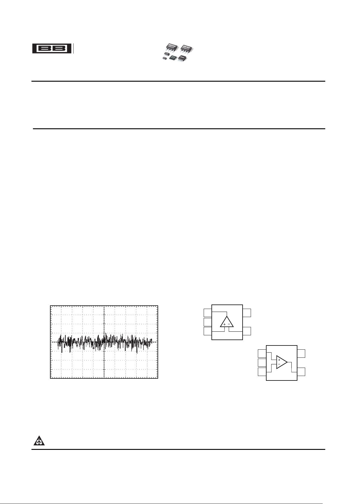
0.1HzTO10HzNOISE
500nV/div
1s/div
1
2
3
5
4
V+
-IN
OUT
V-
+IN
OPA333
SOT23-5
1
2
3
5
4
V+
OUT
+IN
V-
-IN
OPA333
SC70-5
OPA333
OPA2333
SBOS351C – MARCH 2006 – REVISED MAY 2007
1.8V, microPOWER
CMOS OPERATIONAL AMPLIFIERS
Zerø-Drift Series
• LOW OFFSET VOLTAGE: 10 μ V (max)
The OPA333 series of CMOS operational amplifiers
uses a proprietary auto-calibration technique to
• ZERO DRIFT: 0.05 μ V/ ° C (max)
simultaneously provide very low offset voltage (10 μ V
• 0.01Hz to 10Hz NOISE: 1.1 μ V
PP
max) and near-zero drift over time and temperature.
• QUIESCENT CURRENT: 17 μ A
These miniature, high-precision, low quiescent
• SINGLE-SUPPLY OPERATION current amplifiers offer high-impedance inputs that
have a common-mode range 100mV beyond the rails
• SUPPLY VOLTAGE: 1.8V to 5.5V
and rail-to-rail output that swings within 50mV of the
• RAIL-TO-RAIL INPUT/OUTPUT
rails. Single or dual supplies as low as +1.8V ( ± 0.9V)
• microSIZE PACKAGES: SC70 and SOT23
and up to +5.5V ( ± 2.75V) may be used. They are
optimized for low-voltage, single-supply operation.
The OPA333 family offers excellent CMRR without
• TRANSDUCER APPLICATIONS
the crossover associated with traditional
• TEMPERATURE MEASUREMENTS complementary input stages. This design results in
superior performance for driving analog-to-digital
• ELECTRONIC SCALES
converters (ADCs) without degradation of differential
• MEDICAL INSTRUMENTATION
linearity.
• BATTERY-POWERED INSTRUMENTS
The OPA333 (single version) is available in the
• HANDHELD TEST EQUIPMENT
SC70-5, SOT23-5, and SO-8 packages. The
OPA2333 (dual version) is offered in DFN-8 (3mm ×
3mm), MSOP-8, and SO-8 packages. All versions
are specified for operation from –40 ° C to +125 ° C.
Please be aware that an important notice concerning availability, standard warranty, and use in critical applications of Texas
Instruments semiconductor products and disclaimers thereto appears at the end of this data sheet.
PRODUCTION DATA information is current as of publication date.
Copyright © 2006–2007, Texas Instruments Incorporated
Products conform to specifications per the terms of the Texas
Instruments standard warranty. Production processing does not
necessarily include testing of all parameters.
Page 2
www.ti.com
ABSOLUTE MAXIMUM RATINGS
(1)
OPA333
OPA2333
SBOS351C – MARCH 2006 – REVISED MAY 2007
This integrated circuit can be damaged by ESD. Texas Instruments recommends that all integrated circuits be handled with
appropriate precautions. Failure to observe proper handling and installation procedures can cause damage.
ESD damage can range from subtle performance degradation to complete device failure. Precision integrated circuits may be
more susceptible to damage because very small parametric changes could cause the device not to meet its published
specifications.
ORDERING INFORMATION
(1)
PRODUCT PACKAGE-LEAD PACKAGE DESIGNATOR PACKAGE MARKING
SOT23-5 DBV OAXQ
OPA333 SC70-5 DCK BQY
SO-8 D O333A
SO-8 D O2333A
OPA2333 DFN-8 DRB BQZ
MSOP-8 DGK OBAQ
(1) For the most current package and ordering information see the Package Option Addendum at the end of this document, or see the TI
web site at www.ti.com .
OPA333, OPA2333 UNIT
Supply Voltage +7 V
Signal Input Terminals, Voltage
(2)
–0.3 to (V+) + 0.3 V
Signal Input Terminals, Voltage
(2)
± 10 mA
Output Short-Circuit
(3)
Continuous
Operating Temperature –40 to +150 ° C
Storage Temperature –65 to +150 ° C
Junction Temperature +150 ° C
ESD Ratings:
Human Body Model (HBM) 4000 V
Charged Device Model (CDM) 1000 V
Machine Model (MM) 400 V
(1) Stresses above these ratings may cause permanent damage. Exposure to absolute maximum conditions for extended periods may
degrade device reliability. These are stress ratings only, and functional operation of the device at these or any other conditions beyond
those specified is not supported.
(2) Input terminals are diode-clamped to the power-supply rails. Input signals that can swing more than 0.3V beyond the supply rails should
be current limited to 10mA or less.
(3) Short-circuit to ground, one amplifier per package.
2
Submit Documentation Feedback
Page 3
www.ti.com
ELECTRICAL CHARACTERISTICS: V
S
= +1.8V to +5.5V
OPA333
OPA2333
SBOS351C – MARCH 2006 – REVISED MAY 2007
Boldface limits apply over the specified temperature range, TA= –40 ° C to +125 ° C.
At TA= +25 ° C, RL= 10k Ω connected to VS/2, V
CM
= VS/2, and V
OUT
= VS/2, unless otherwise noted.
OPA333, OPA2333
PARAMETER TEST CONDITIONS MIN TYP MAX UNIT
OFFSET VOLTAGE
Input Offset Voltage V
OS
VS= +5V 2 10 μ V
vs Temperature dV
OS
/dT 0.02 0.05 μ V/ ° C
vs Power Supply PSRR VS= +1.8V to +5.5V 1 5 μ V/V
Long-Term Stability
(1)
See
(1)
Channel Separation, dc 0.1 μ V/V
INPUT BIAS CURRENT
Input Bias Current I
B
± 70 ± 200 pA
over Temperature ± 150 pA
Input Offset Current I
OS
± 140 ± 400 pA
NOISE
Input Voltage Noise, f = 0.01Hz to 1Hz 0.3 μ V
PP
Input Voltage Noise, f = 0.1Hz to 10Hz 1.1 μ V
PP
Input Current Noise, f = 10Hz i
n
100 fA/ √ Hz
INPUT VOLTAGE RANGE
Common-Mode Voltage Range V
CM
(V–) – 0.1 (V+) + 0.1 V
Common-Mode Rejection Ratio CMRR (V–) – 0.1V < VCM< (V+) + 0.1V 106 130 dB
INPUT CAPACITANCE
Differential 2 pF
Common-Mode 4 pF
OPEN-LOOP GAIN
(V–) + 100mV < VO< (V+) – 100mV, RL=
Open-Loop Voltage Gain A
OL
106 130 dB
10k Ω
FREQUENCY RESPONSE
Gain-Bandwidth Product GBW CL= 100pF 350 kHz
Slew Rate SR G = +1 0.16 V/ μ s
OUTPUT
Voltage Output Swing from Rail RL= 10k Ω 30 50 mV
over Temperature RL= 10k Ω 70 mV
Short-Circuit Current I
SC
± 5 mA
Capacitive Load Drive C
L
See Typical Characteristics
Open-Loop Output Impedance f = 350kHz, IO= 0 2 k Ω
POWER SUPPLY
Specified Voltage Range V
S
1.8 5.5 V
Quiescent Current Per Amplifier I
Q
IO= 0 17 25 μ A
over Temperature 28 μ A
Turn-On Time VS= +5V 100 μ s
TEMPERATURE RANGE
Specified Range –40 +125 ° C
Operating Range –40 +150 ° C
Storage Range –65 +150 ° C
Thermal Resistance θ
JA
° C/W
SOT23-5 200 ° C/W
MSOP-8, SO-8 150 ° C/W
DFN-8 50 ° C/W
SC70-5 250 ° C/W
(1) 300-hour life test at +150 ° C demonstrated randomly distributed variation of approximately 1 μ V.
3
Submit Documentation Feedback
Page 4
www.ti.com
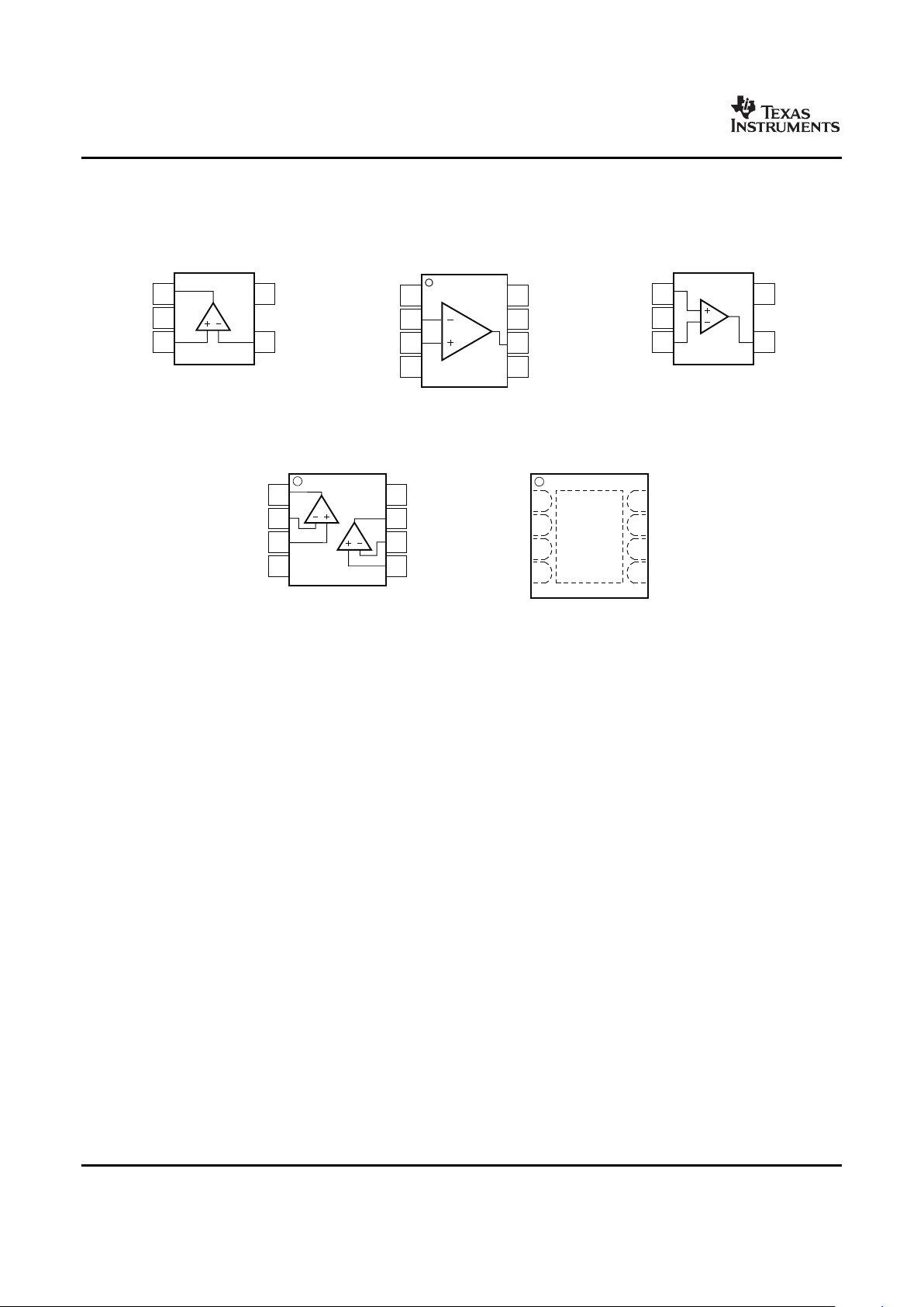
PIN CONFIGURATIONS
1
2
3
5
4
V+
-IN
OUT
V-
+IN
1
2
3
5
4
V+
OUT
+IN
V-
-IN
1
2
3
4
8
7
6
5
NC
(1)
V+
OUT
NC
(1)
NC
(1)
-IN
+IN
V-
1
2
3
4
8
7
6
5
V+
OUTB
-INB
+INB
OUTA
-INA
+INA
V-
A
B
1
2
3
4
8
7
6
5
V+
OUTB
-INB
+INB
OUTA
-INA
+INA
V-
Exposed
Thermal
DiePad
on
Underside
(2)
OPA333
OPA2333
SBOS351C – MARCH 2006 – REVISED MAY 2007
OPA333 OPA333 OPA333
SOT23-5 SO-8 SC70-5
Top View Top View Top View
OPA2333 OPA2333
SO-8, MSOP-8 DFN-8
Top View Top View
1. NC denotes no internal connection.
2. Connect thermal die pad to V–.
4
Submit Documentation Feedback
Page 5
www.ti.com
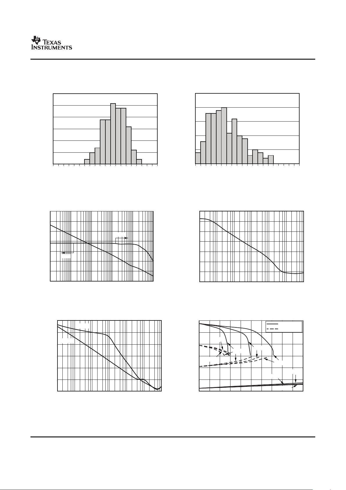
TYPICAL CHARACTERISTICS
Population
-10
-9
-
8
-
7
-
6
-
5
-
4
-
3
-
2
-
1
0
1
2
3
4
5
6
7
8
9
10
OffsetVoltage( V)m
Population
0
0.0025
0.0050
0.0075
0.0100
0.0125
0.0150
0.0175
0.0200
0.0225
0.0250
0.0275
0.0300
0.0325
0.0350
0.0375
0.0400
0.0425
0.0450
0.0475
0.0500
OffsetVoltageDrift( V/ C)m °
A (dB)
OL
10
120
100
80
60
40
20
0
-20
Phase( )°
250
200
150
100
50
0
-50
-100
100k10k1k100
Frequency(Hz)
1M
Phase
Gain
CMRR(dB)
1
140
120
100
80
60
40
20
0
100k10k1k10010
Frequency(Hz)
1M
PSRR(dB)
1
120
100
80
60
40
20
0
10k 100k1k10010
Frequency(Hz)
1M
+PSRR
-PSRR
OutputSwing(V)
0
3
2
1
0
-1
-2
-3
1
OutputCurrent(mA)
107 8 965432
- °40 C
- °40 C
- °40 C
+25 C°
+25 C°
+25 C°
+125 C°
+125 C°
V = 2.75V±
S
V = 0.9V±
S
OPA333
OPA2333
SBOS351C – MARCH 2006 – REVISED MAY 2007
At TA= +25 ° C, VS= +5V, and CL= 0pF, unless otherwise noted.
OFFSET VOLTAGE PRODUCTION DISTRIBUTION OFFSET VOLTAGE DRIFT PRODUCTION DISTRIBUTION
Figure 1. Figure 2.
OPEN-LOOP GAIN vs FREQUENCY COMMON-MODE REJECTION RATIO vs FREQUENCY
Figure 3. Figure 4.
POWER-SUPPLY REJECTION RATIO vs FREQUENCY OUTPUT VOLTAGE SWING vs OUTPUT CURRENT
Figure 5. Figure 6.
5
Submit Documentation Feedback
Page 6
www.ti.com
I
(pA)
B
0
100
80
60
40
20
0
-20
-40
-60
-80
-100
1
Common-ModeVoltage(V)
5432
-I
B
+I
B
I
(pA)
B
-50
200
150
100
50
0
-50
-100
-150
-200
-25
Temperature( C)°
1251007550250
V =5.5V
S
V =1.8V
S
-I
B
-I
B
+I
B
+I
B
OutputVoltage(1V/div)
Time(50 s/div)m
G=1
R =10kW
L
I ( A)m
Q
-50
25
20
15
10
5
0
-25
Temperature( C)°
1251007550250
V =1.8V
S
V =5.5V
S
OutputVoltage(50mV/div)
Time(5 s/div)m
G=+1
R =10kW
L
2V/div
0
1V/div
0
Time(50 s/div)m
Input
Output
10kW
1kW
OPA333
+2.5V
-2.5V
OPA333
OPA2333
SBOS351C – MARCH 2006 – REVISED MAY 2007
TYPICAL CHARACTERISTICS (continued)
At TA= +25 ° C, VS= +5V, and CL= 0pF, unless otherwise noted.
INPUT BIAS CURRENT vs COMMON-MODE VOLTAGE INPUT BIAS CURRENT vs TEMPERATURE
Figure 7. Figure 8.
QUIESCENT CURRENT vs TEMPERATURE LARGE-SCALE STEP RESPONSE
Figure 9. Figure 10.
SMALL-SCALE STEP RESPONSE POSITIVE OVER-VOLTAGE RECOVERY
Figure 11. Figure 12.
6
Submit Documentation Feedback
Page 7
www.ti.com
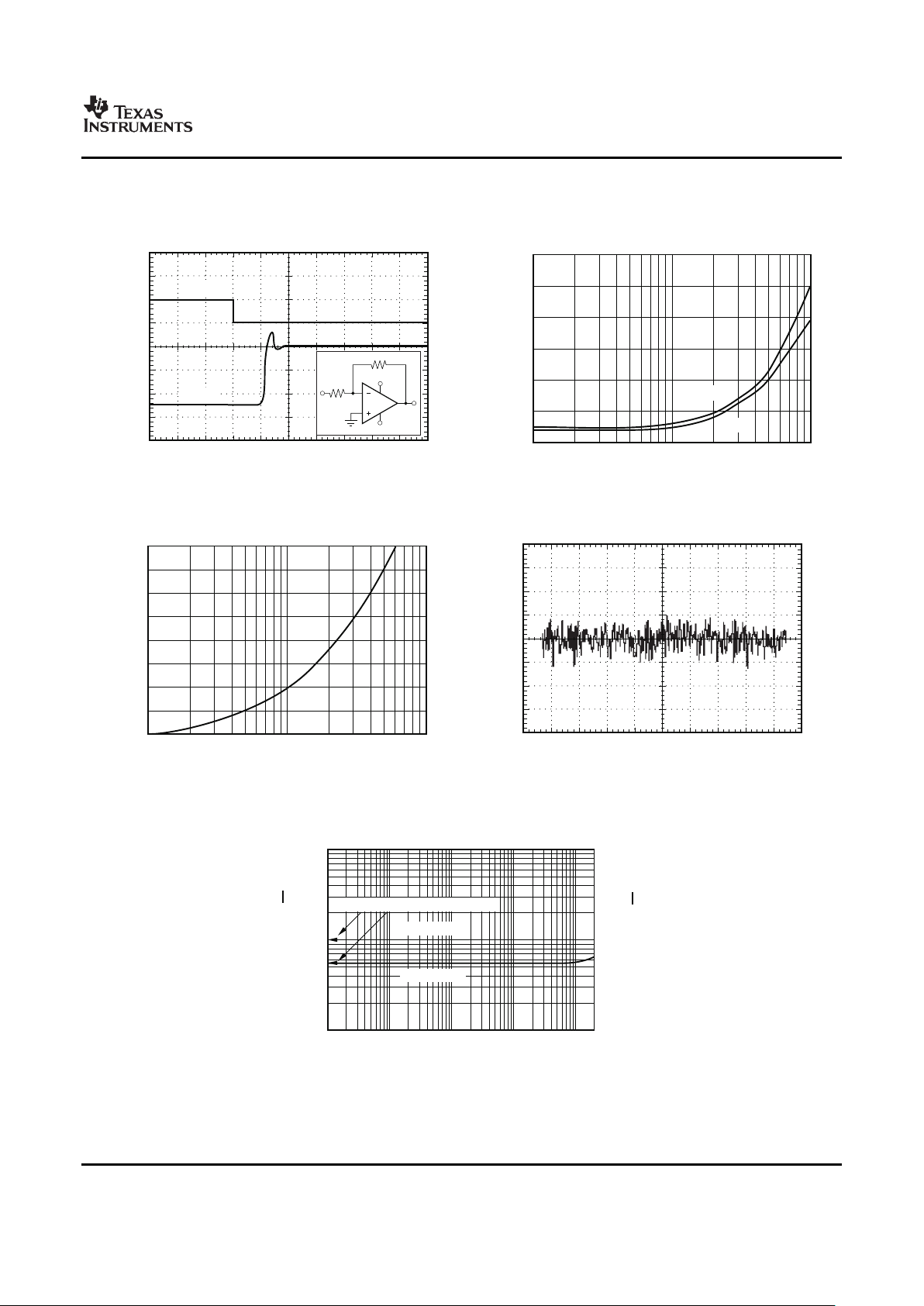
2V/div
0
1V/div
0
Time(50 s/div)m
Input
Output
10kW
1kW
OPA333
+2.5V
-2.5V
SettlingTime( s)
m
1
600
500
400
300
200
100
0
10
Gain(dB)
100
0.001%
0.01%
4VStep
500nV/div
1s/div
Overshoot(%)
10
40
35
30
25
20
15
10
5
0
100
LoadCapacitance(pF)
1000
VoltageNoise(nV/ )ÖHz
1
1000
100
10
CurrentNoise(fA/
)ÖHz
1000
100
10
1k10010
Frequency(Hz)
10k
CurrentNoise
VoltageNoise
Continueswithno1/f(flicker)noise.
OPA333
OPA2333
SBOS351C – MARCH 2006 – REVISED MAY 2007
TYPICAL CHARACTERISTICS (continued)
At TA= +25 ° C, VS= +5V, and CL= 0pF, unless otherwise noted.
NEGATIVE OVER-VOLTAGE RECOVERY SETTLING TIME vs CLOSED-LOOP GAIN
Figure 13. Figure 14.
SMALL-SIGNAL OVERSHOOT vs LOAD CAPACITANCE 0.1Hz TO 10Hz NOISE
Figure 15. Figure 16.
CURRENT AND VOLTAGE NOISE SPECTRAL DENSITY vs
FREQUENCY
Figure 17.
7
Submit Documentation Feedback
Page 8

www.ti.com
APPLICATIONS INFORMATION
INPUT VOLTAGE
5kW
OPA333
10mAmax
+5V
V
IN
V
OUT
I
OVERLOAD
Current-limitingresistor
requiredifinputvoltage
exceedssupplyrailsby
³ 0.5V.
OPERATING VOLTAGE
INTERNAL OFFSET CORRECTION
OPA333
OPA2333
SBOS351C – MARCH 2006 – REVISED MAY 2007
The OPA333 and OPA2333 are unity-gain stable and
free from unexpected output phase reversal. They
use a proprietary auto-calibration technique to
The OPA333 and OPA2333 input common-mode
provide low offset voltage and very low drift over time
voltage range extends 0.1V beyond the supply rails.
and temperature. For lowest offset voltage and
The OPA333 is designed to cover the full range
precision performance, circuit layout and mechanical
without the troublesome transition region found in
conditions should be optimized. Avoid temperature
some other rail-to-rail amplifiers.
gradients that create thermoelectric (Seebeck)
Normally, input bias current is about 70pA; however,
effects in the thermocouple junctions formed from
input voltages exceeding the power supplies can
connecting dissimilar conductors. These
cause excessive current to flow into or out of the
thermally-generated potentials can be made to
input pins. Momentary voltages greater than the
cancel by assuring they are equal on both input
power supply can be tolerated if the input current is
terminals. Other layout and design considerations
limited to 10mA. This limitation is easily
include:
accomplished with an input resistor, as shown in
• Use low thermoelectric-coefficient conditions
Figure 18 .
(avoid dissimilar metals).
• Thermally isolate components from power
supplies or other heat sources.
• Shield op amp and input circuitry from air
currents, such as cooling fans.
Following these guidelines will reduce the likelihood
of junctions being at different temperatures, which
can cause thermoelectric voltages of 0.1 μ V/ ° C or
higher, depending on materials used.
Figure 18. Input Current Protection
The OPA333 and OPA2333 op amps operate over a
power-supply range of +1.8V to +5.5V ( ± 0.9V to
± 2.75V). Supply voltages higher than +7V (absolute
maximum) can permanently damage the device.
The OPA333 and OPA2333 op amps use an
Parameters that vary over supply voltage or
auto-calibration technique with a time-continuous
temperature are shown in the Typical Characteristics
350kHz op amp in the signal path. This amplifier is
section of this data sheet.
zero-corrected every 8 μ s using a proprietary
technique. Upon power-up, the amplifier requires
approximately 100 μ s to achieve specified V
OS
accuracy. This design has no aliasing or flicker
noise.
8
Submit Documentation Feedback
Page 9

www.ti.com
ACHIEVING OUTPUT SWING TO THE OP
GENERAL LAYOUT GUIDELINES
V
OUT
R =20kW
P
OpAmpV =GND-
OPA333
V
IN
V+=+5V
-5V
Additional
Negative
Supply
+ +
+
- -
+
4.096V
0.1 Fm
+5V
ZeroAdj.
K-Type
Thermocouple
40.7 V/ Cm °
R
2
549W
R
9
150kW
R
5
31.6kW
R
1
6.04kW
R
6
200W
+5V
0.1 Fm
R
2
2.94kW
V
O
R
3
60.4W
R
4
6.04kW
OPA333
D1
REF3140
OPA333
OPA2333
SBOS351C – MARCH 2006 – REVISED MAY 2007
works with some types of output stages. The
AMP NEGATIVE RAIL OPA333 and OPA2333 have been characterized to
perform with this technique; the recommended
Some applications require output voltage swings
resistor value is approximately 20k Ω . Note that this
from 0V to a positive full-scale voltage (such as
configuration will increase the current consumption
+2.5V) with excellent accuracy. With most
by several hundreds of microamps. Accuracy is
single-supply op amps, problems arise when the
excellent down to 0V and as low as –2mV. Limiting
output signal approaches 0V, near the lower output
and nonlinearity occurs below –2mV, but excellent
swing limit of a single-supply op amp. A good
accuracy returns as the output is again driven above
single-supply op amp may swing close to
–2mV. Lowering the resistance of the pull-down
single-supply ground, but will not reach ground. The
resistor will allow the op amp to swing even further
output of the OPA333 and OPA2333 can be made to
below the negative rail. Resistances as low as 10k Ω
swing to ground, or slightly below, on a single-supply
can be used to achieve excellent accuracy down to
power source. To do so requires the use of another
–10mV.
resistor and an additional, more negative, power
supply than the op amp negative supply. A pull-down
resistor may be connected between the output and
the additional negative supply to pull the output down
Attention to good layout practices is always
below the value that the output would otherwise
recommended. Keep traces short and, when
achieve, as shown in Figure 19 .
possible, use a printed circuit board (PCB) ground
plane with surface-mount components placed as
close to the device pins as possible. Place a 0.1 μ F
capacitor closely across the supply pins. These
guidelines should be applied throughout the analog
circuit to improve performance and provide benefits
such as reducing the EMI
(electromagnetic-interference) susceptibility.
Operational amplifiers vary in their susceptibility to
radio frequency interference (RFI). RFI can generally
be identified as a variation in offset voltage or dc
signal levels with changes in the interfering RF
signal. The OPA333 has been specifically designed
to minimize susceptibility to RFI and demonstrates
Figure 19. For V
OUT
Range to Ground
remarkably low sensitivity compared to previous
generation devices. Strong RF fields may still cause
varying offset levels.
The OPA333 and OPA2333 have an output stage
that allows the output voltage to be pulled to its
negative supply rail, or slightly below, using the
technique previously described. This technique only
Figure 20. Temperature Measurement
9
Submit Documentation Feedback
Page 10
www.ti.com
R
1
V
EX
V
OUT
V
REF
R
1
OPA333
R
R
R R
+5V
NOTE:1%resistorsprovideadequatecommon-moderejectionatsmallground-looperrors.
OPA333
ADS1100
Load
V
I C
2
R
1
4.99kW
R
3
4.99kW
R
4
48.7kW
R
2
49.9kW
+5V
3V
REF3130
R
7
1.18kW
R
SHUNT
1W
R
6
71.5kW
R
N
56W
R
N
56W
(PGAGain=4)
FS=3.0V
StrayGround-LoopResistance
I
LOAD
OPA333
Output
R
SHUNT
Load
V+
V+
R
G
R
L
R
(2)
1
10kW
R
BIAS
+5V
zener
(1)
Twozener
biasingmethods
areshown.
(3)
MOSFETratedto
stand-offsupplyvoltage
suchasBSS84for
upto50V.
(1)zenerratedforopampsupplycapability(thatis,5.1VforOPA333).
(2)Current-limitingresistor.
(3)ChoosezenerbiasingresistorordualNMOSFETs(FDG6301N,NTJD4001N,orSi1034)
NOTES:
OPA333
OPA2333
SBOS351C – MARCH 2006 – REVISED MAY 2007
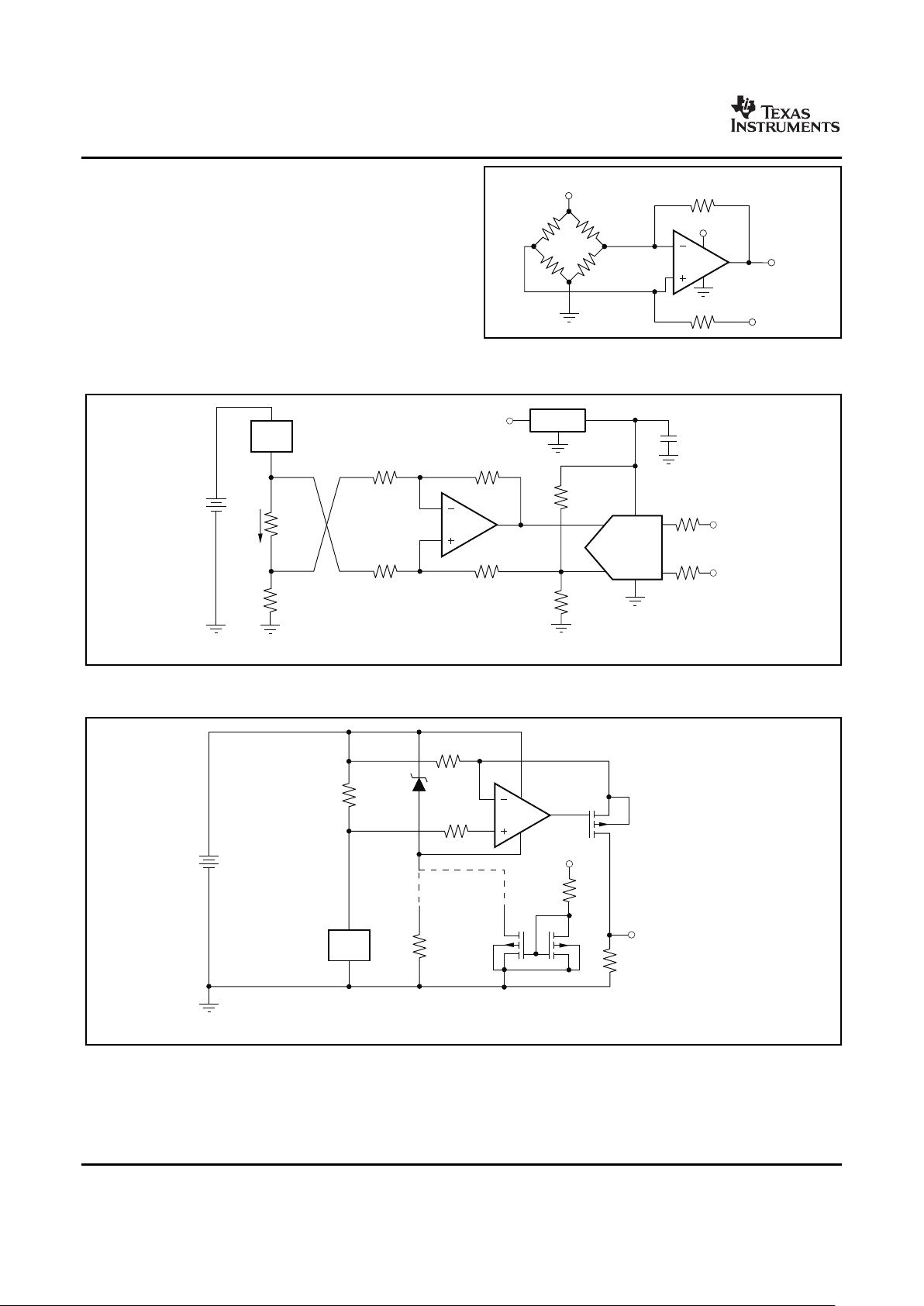
Figure 21 shows the basic configuration for a bridge
amplifier.
A low-side current shunt monitor is shown in
Figure 22 . R
N
are operational resistors used to
isolate the ADS1100 from the noise of the digital I2C
bus. Since the ADS1100 is a 16-bit converter, a
precise reference is essential for maximum accuracy.
If absolute accuracy is not required, and the 5V
power supply is sufficiently stable, the REF3130 may
be omitted.
Figure 21. Single Op Amp Bridge Amplifier
Figure 22. Low-Side Current Monitor
Figure 23. High-Side Current Monitor
10
Submit Documentation Feedback
Page 11

www.ti.com
V
1
-In
V
2
+In
R
1
R
2
2
3
5
6
1
R
2
OPA333
OPA333
INA152
V
O
V =(1+2R /R
O 2 1 2 1
)(V V )-
OPA333
3V
1MW 60kW
100kW
1MW
NTC
Thermistor
R
1
100kW
1/2
OPA2333
RA
Inverted
V
CM
+V
S
INA321
(1)
+VS
V
OUT
+V
S
+V
S
+V
S
OPA333
+V
S
1/2V
S
dc
3
2
1
4
5
6
G =1kV/V
TOT
G =5
INA
G =200
OPA
f =150Hz
LPF
f =0.5Hz
HPF
(providesacsignalcoupling)
V =+2.7Vto+5.5V
S
BW=0.5Hzto150Hz
f =0.5Hz
O
Wilson
V
CENTRAL
(RA+LA+LL)/3
7
ac
1/2V
S
R
2
100kW
1/2
OPA2333
LL
+V
S
R
3
100kW
1/2
OPA2333
LA
R
4
100kW
R
9
20kW
R
6
100kW
RL
+V
S
+V
S
1/2
OPA2333
1/2
OPA2333
1/2
OPA2333
C
4
1.06nF
C
3
1 Fm
R
14
1MW
R
12
5kW
R
13
318kW
R
7
100kW
R
8
100kW
R
10
1MW
C
2
0.64 Fm
R
11
1MW
C
1
47pF
R
5
390kW
NOTE:(1)Otherinstrumentationamplifierscanbeused,
suchastheINA326,whichhaslowernoise,
buthigherquiescentcurrent.
OPA333
OPA2333
SBOS351C – MARCH 2006 – REVISED MAY 2007
Figure 24. Thermistor Measurement Figure 25. Precision Instrumentation Amplifier
Figure 26. Single-Supply, Very Low Power, ECG Circuit
11
Submit Documentation Feedback
Page 12

www.ti.com
DFN PACKAGE DFN LAYOUT GUIDELINES
OPA333
OPA2333
SBOS351C – MARCH 2006 – REVISED MAY 2007
The OPA2333 is offered in an DFN-8 package (also The exposed leadframe die pad on the DFN package
known as SON). The DFN is a QFN package with should be soldered to a thermal pad on the PCB. A
lead contacts on only two sides of the bottom of the mechanical drawing showing an example layout is
package. This leadless package maximizes board attached at the end of this data sheet. Refinements
space and enhances thermal and electrical to this layout may be necessary based on assembly
characteristics through an exposed pad. process requirements. Mechanical drawings located
at the end of this data sheet list the physical
DFN packages are physically small, have a smaller
dimensions for the package and pad. The five holes
routing area, improved thermal performance, and
in the landing pattern are optional, and are intended
improved electrical parasitics. Additionally, the
for use with thermal vias that connect the leadframe
absence of external leads eliminates bent-lead
die pad to the heatsink area on the PCB.
issues.
Soldering the exposed pad significantly improves
The DFN package can be easily mounted using
board-level reliability during temperature cycling, key
standard printed circuit board (PCB) assembly
push, package shear, and similar board-level tests.
techniques. See Application Note QFN/SON PCB
Even with applications that have low-power
Attachment (SLUA271 ) and Application Report Quad
dissipation, the exposed pad must be soldered to the
Flatpack No-Lead Logic Packages (SCBA017 ), both
PCB to provide structural integrity and long-term
available for download at www.ti.com .
reliability.
The exposed leadframe die pad on the bottom of
the package should be connected to V– or left
unconnected.
12
Submit Documentation Feedback
Page 13

PACKAGING INFORMATION
Orderable Device Status
(1)
Package
Type
Package
Drawing
Pins Package
Qty
Eco Plan
(2)
Lead/Ball Finish MSL Peak Temp
(3)
OPA2333AID ACTIVE SOIC D 8 75 Green (RoHS &
no Sb/Br)
CU NIPDAU Level-1-260C-UNLIM
OPA2333AIDG4 ACTIVE SOIC D 8 75 Green (RoHS &
no Sb/Br)
CU NIPDAU Level-1-260C-UNLIM
OPA2333AIDGKR ACTIVE MSOP DGK 8 2500 Green (RoHS &
no Sb/Br)
CU NIPDAU Level-2-260C-1 YEAR
OPA2333AIDGKRG4 ACTIVE MSOP DGK 8 2500 Green (RoHS &
no Sb/Br)
CU NIPDAU Level-2-260C-1 YEAR
OPA2333AIDGKT ACTIVE MSOP DGK 8 250 Green (RoHS &
no Sb/Br)
CU NIPDAU Level-2-260C-1 YEAR
OPA2333AIDGKTG4 ACTIVE MSOP DGK 8 250 Green (RoHS &
no Sb/Br)
CU NIPDAU Level-2-260C-1 YEAR
OPA2333AIDR ACTIVE SOIC D 8 2500 Green (RoHS &
no Sb/Br)
CU NIPDAU Level-1-260C-UNLIM
OPA2333AIDRBR ACTIVE SON DRB 8 3000 Green (RoHS &
no Sb/Br)
CU NIPDAU Level-2-260C-1 YEAR
OPA2333AIDRBRG4 ACTIVE SON DRB 8 3000 Green (RoHS &
no Sb/Br)
CU NIPDAU Level-2-260C-1 YEAR
OPA2333AIDRBT ACTIVE SON DRB 8 250 Green (RoHS &
no Sb/Br)
CU NIPDAU Level-2-260C-1 YEAR
OPA2333AIDRBTG4 ACTIVE SON DRB 8 250 Green (RoHS &
no Sb/Br)
CU NIPDAU Level-2-260C-1 YEAR
OPA2333AIDRG4 ACTIVE SOIC D 8 2500 Green (RoHS &
no Sb/Br)
CU NIPDAU Level-1-260C-UNLIM
OPA333AID ACTIVE SOIC D 8 75 Green (RoHS &
no Sb/Br)
CU NIPDAU Level-1-260C-UNLIM
OPA333AIDBVR ACTIVE SOT-23 DBV 5 3000 Green (RoHS &
no Sb/Br)
CU NIPDAU Level-1-260C-UNLIM
OPA333AIDBVRG4 ACTIVE SOT-23 DBV 5 3000 Green (RoHS &
no Sb/Br)
CU NIPDAU Level-1-260C-UNLIM
OPA333AIDBVT ACTIVE SOT-23 DBV 5 250 Green (RoHS &
no Sb/Br)
CU NIPDAU Level-1-260C-UNLIM
OPA333AIDBVTG4 ACTIVE SOT-23 DBV 5 250 Green (RoHS &
no Sb/Br)
CU NIPDAU Level-1-260C-UNLIM
OPA333AIDCKR ACTIVE SC70 DCK 5 3000 Green (RoHS &
no Sb/Br)
CU NIPDAU Level-1-260C-UNLIM
OPA333AIDCKRG4 ACTIVE SC70 DCK 5 3000 Green (RoHS &
no Sb/Br)
CU NIPDAU Level-1-260C-UNLIM
OPA333AIDCKT ACTIVE SC70 DCK 5 250 Green (RoHS &
no Sb/Br)
CU NIPDAU Level-1-260C-UNLIM
OPA333AIDCKTG4 ACTIVE SC70 DCK 5 250 Green (RoHS &
no Sb/Br)
CU NIPDAU Level-1-260C-UNLIM
OPA333AIDG4 ACTIVE SOIC D 8 75 Green (RoHS &
no Sb/Br)
CU NIPDAU Level-1-260C-UNLIM
OPA333AIDR ACTIVE SOIC D 8 2500 Green (RoHS &
no Sb/Br)
CU NIPDAU Level-1-260C-UNLIM
OPA333AIDRG4 ACTIVE SOIC D 8 2500 Green (RoHS &
no Sb/Br)
CU NIPDAU Level-1-260C-UNLIM
(1)
The marketing status values are defined as follows:
PACKAGE OPTION ADDENDUM
www.ti.com
25-Apr-2007
Addendum-Page 1
Page 14

ACTIVE: Product device recommended for new designs.
LIFEBUY: TI has announced that the device will be discontinued, and a lifetime-buy period is in effect.
NRND: Not recommended for new designs. Device is in production to support existing customers, but TI does not recommend using this part in
a new design.
PREVIEW: Device has been announced but is not in production. Samples may or may not be available.
OBSOLETE: TI has discontinued the production of the device.
(2)
Eco Plan - The planned eco-friendly classification: Pb-Free (RoHS), Pb-Free (RoHS Exempt), or Green (RoHS & no Sb/Br) - please check
http://www.ti.com/productcontent for the latest availability information and additional product content details.
TBD: The Pb-Free/Green conversion plan has not been defined.
Pb-Free (RoHS): TI's terms "Lead-Free" or "Pb-Free" mean semiconductor products that are compatible with the current RoHS requirements
for all 6 substances, including the requirement that lead not exceed 0.1% by weight in homogeneous materials. Where designed to be soldered
at high temperatures, TI Pb-Free products are suitable for use in specified lead-free processes.
Pb-Free (RoHS Exempt): This component has a RoHS exemption for either 1) lead-based flip-chip solder bumps used between the die and
package, or 2) lead-based die adhesive used between the die and leadframe. The component is otherwise considered Pb-Free (RoHS
compatible) as defined above.
Green (RoHS & no Sb/Br): TI defines "Green" to mean Pb-Free (RoHS compatible), and free of Bromine (Br) and Antimony (Sb) based flame
retardants (Br or Sb do not exceed 0.1% by weight in homogeneous material)
(3)
MSL, Peak Temp. -- The Moisture Sensitivity Level rating according to the JEDEC industry standard classifications, and peak solder
temperature.
Important Information and Disclaimer:The information provided on this page represents TI's knowledge and belief as of the date that it is
provided. TI bases its knowledge and belief on information provided by third parties, and makes no representation or warranty as to the
accuracy of such information. Efforts are underway to better integrate information from third parties. TI has taken and continues to take
reasonable steps to provide representative and accurate information but may not have conducted destructive testing or chemical analysis on
incoming materials and chemicals. TI and TI suppliers consider certain information to be proprietary, and thus CAS numbers and other limited
information may not be available for release.
In no event shall TI's liability arising out of such information exceed the total purchase price of the TI part(s) at issue in this document sold by TI
to Customer on an annual basis.
PACKAGE OPTION ADDENDUM
www.ti.com
25-Apr-2007
Addendum-Page 2
Page 15

Page 16

Page 17

Page 18

Page 19

Page 20

Page 21

Page 22

IMPORTANT NOTICE
Texas Instruments Incorporated and its subsidiaries (TI) reserve the right to make corrections, modifications, enhancements,
improvements, and other changes to its products and services at any time and to discontinue any product or service without notice.
Customers should obtain the latest relevant information before placing orders and should verify that such information is current and
complete. All products are sold subject to TI’s terms and conditions of sale supplied at the time of order acknowledgment.
TI warrants performance of its hardware products to the specifications applicable at the time of sale in accordance with TI’s
standard warranty. Testing and other quality control techniques are used to the extent TI deems necessary to support this
warranty. Except where mandated by government requirements, testing of all parameters of each product is not necessarily
performed.
TI assumes no liability for applications assistance or customer product design. Customers are responsible for their products and
applications using TI components. To minimize the risks associated with customer products and applications, customers should
provide adequate design and operating safeguards.
TI does not warrant or represent that any license, either express or implied, is granted under any TI patent right, copyright, mask
work right, or other TI intellectual property right relating to any combination, machine, or process in which TI products or services
are used. Information published by TI regarding third-party products or services does not constitute a license from TI to use such
products or services or a warranty or endorsement thereof. Use of such information may require a license from a third party under
the patents or other intellectual property of the third party, or a license from TI under the patents or other intellectual property of TI.
Reproduction of TI information in TI data books or data sheets is permissible only if reproduction is without alteration and is
accompanied by all associated warranties, conditions, limitations, and notices. Reproduction of this information with alteration is an
unfair and deceptive business practice. TI is not responsible or liable for such altered documentation. Information of third parties
may be subject to additional restrictions.
Resale of TI products or services with statements different from or beyond the parameters stated by TI for that product or service
voids all express and any implied warranties for the associated TI product or service and is an unfair and deceptive business
practice. TI is not responsible or liable for any such statements.
TI products are not authorized for use in safety-critical applications (such as life support) where a failure of the TI product would
reasonably be expected to cause severe personal injury or death, unless officers of the parties have executed an agreement
specifically governing such use. Buyers represent that they have all necessary expertise in the safety and regulatory ramifications
of their applications, and acknowledge and agree that they are solely responsible for all legal, regulatory and safety-related
requirements concerning their products and any use of TI products in such safety-critical applications, notwithstanding any
applications-related information or support that may be provided by TI. Further, Buyers must fully indemnify TI and its
representatives against any damages arising out of the use of TI products in such safety-critical applications.
TI products are neither designed nor intended for use in military/aerospace applications or environments unless the TI products are
specifically designated by TI as military-grade or "enhanced plastic." Only products designated by TI as military-grade meet military
specifications. Buyers acknowledge and agree that any such use of TI products which TI has not designated as military-grade is
solely at the Buyer's risk, and that they are solely responsible for compliance with all legal and regulatory requirements in
connection with such use.
TI products are neither designed nor intended for use in automotive applications or environments unless the specific TI products
are designated by TI as compliant with ISO/TS 16949 requirements. Buyers acknowledge and agree that, if they use any
non-designated products in automotive applications, TI will not be responsible for any failure to meet such requirements.
Following are URLs where you can obtain information on other Texas Instruments products and application solutions:
Products Applications
Amplifiers amplifier.ti.com Audio www.ti.com/audio
Data Converters dataconverter.ti.com Automotive www.ti.com/automotive
DSP dsp.ti.com Broadband www.ti.com/broadband
Interface interface.ti.com Digital Control www.ti.com/digitalcontrol
Logic logic.ti.com Military www.ti.com/military
Power Mgmt power.ti.com Optical Networking www.ti.com/opticalnetwork
Microcontrollers microcontroller.ti.com Security www.ti.com/security
RFID www.ti-rfid.com Telephony www.ti.com/telephony
Low Power www.ti.com/lpw Video & Imaging www.ti.com/video
Wireless
Wireless www.ti.com/wireless
Mailing Address: Texas Instruments, Post Office Box 655303, Dallas, Texas 75265
Copyright © 2007, Texas Instruments Incorporated
 Loading...