

Page 1
DATA SHEET
HETERO JUNCTION FIELD EFFECT TRANSISTOR
NE325S01
C to Ku BAND SUPER LOW NOISE AMPLIFIER
N-CHANNEL HJ-FET
DESCRIPTION
The NE325S01 is a Hetero Junction FET that utilizes the
hetero junction to create high mobility electrons. Its excellent
low noise and high associated gain make it suitable for DBS
and another commercial systems.
FEATURES
• Super Low Noise Figure & High Associated Gain
NF = 0.45 dB TYP., Ga = 12.5 dB TYP. at f = 12 GHz
• Gate Length : L
• Gate Width : Wg = 200 µm
g ≤ 0.20
µ
m
ORDERING INFORMATION
PART NUMBER SUPPLYING FORM MARKING
NE325S01-T1 Tape & reel 1000 pcs./reel D
NE325S01-T1B Tape & reel 4000 pcs./reel
ABSOLUTE MAXIMUM RATINGS (TA = 25 ˚C)
Drain to Source Voltage VDS 4.0 V
Gate to Source Voltage VGS –3.0 V
Drain Current I
Gate Current IG 100
Total Power Dissipation Ptot 165 mW
Channel Temperature T
Storage Temperature Tstg –65 to +125 ˚ C
D IDSS mA
µ
ch 125 ˚ C
A
2
0.125 ±0.05
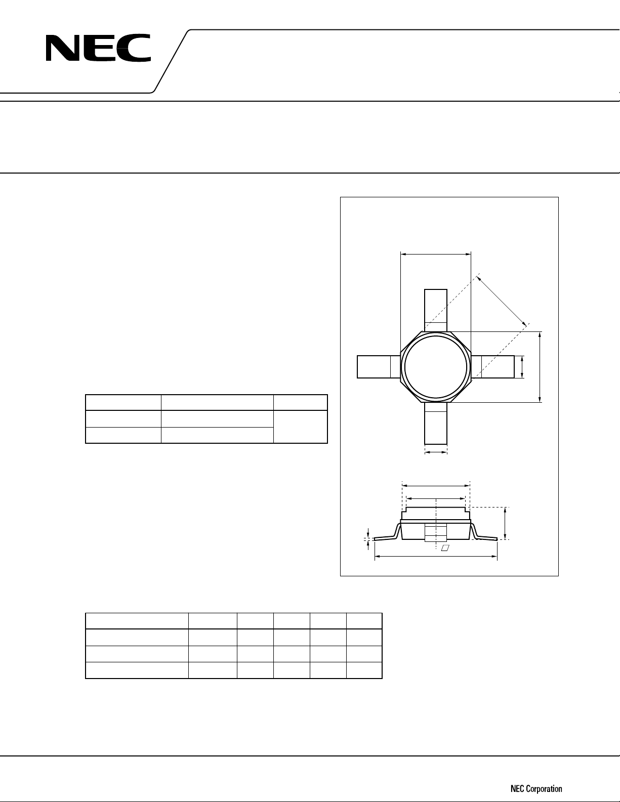
PACKAGE DIMENSIONS
(Unit: mm)
2.0 ±0.2
1
2.0 ±0.2
D
3
0.65 TYP.
1.9 ±0.2
1.6
0.4MAX
4.0 ±0.2
4
1. Source
2. Drain
3. Source
4. Gate
1.5 MAX
2.0 ±0.2
0.5 TYP.
RECOMMENDED OPERATING CONDITION (TA = 25 ˚C)
CHARACTERISTIC SYMBOL MIN. TYP. MAX. Unit
Drain to Source Voltage VDS 23V
Drain Current ID 10 20 mA
Input Power Pin 0 dBm
Document No. P11138EJ3V0DS00 (3rd edition)
Date Published October 1996 N
Printed in Japan
©
1996
Page 2
NE325S01
ELECTRICAL CHARACTERISTICS (TA = 25 ˚C)
CHARACTERISTIC SYMBOL MIN. TYP. MAX. UNIT TEST CONDITIONS
Gate to Source Leak Current IGSO 0.5 10
Saturated Drain Current IDSS 20 60 90 mA VDS = 2 V, VGS = 0 V
Gate to Source Cutoff Voltage VGS(off) –0.2 –0.7 –2.0 V VDS = 2 V, ID = 100 µA
Transconductance gm 45 60 mS VDS = 2V, ID = 10 mA
Noise Figure NF 0.45 0.55 dB VDS = 2 V, ID = 10 mA, f = 12 GHz
Associated Gain Ga 11.0 12.5 dB
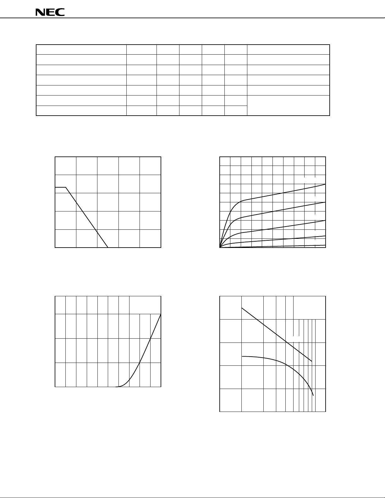
TYPICAL CHARACTERISTICS (TA = 25 ˚C)
µ
AVGS = –3 V
TOTAL POWER DISSIPATION vs.
AMBIENT TEMPERATURE
250
200
150
100
50
Ptot - Total Power Dissipation - mW
0 50 100 150 200 250
T
A - Ambient Temperature - ˚C
DRAIN CURRENT vs.
GATE TO SOURCE VOLTAGE
VDS = 2 V
60
DRAIN CURRENT vs.
DRAIN TO SOURCE VOLTAGE
100
80
60
40
ID - Drain Current - mA
20
0 3.01.5
V
DS - Drain to Source Voltage - V
MAXIMUM AVAILABLE GAIN, FORWARD
INSERTION GAIN vs. FREQUENCY
24
20
MSG.
VGS = 0 V
–0.2 V
–0.4 V
–0.6 V
–0.8 V
VDS = 2 V
I
D = 10 mA
40
20
ID - Drain Current - mA
0
–2.0 –1.0 0
V
GS - Gate to Source Voltage - V
2
16
2
12
- Forward Insertion Gain - dB
2
8
21s|
MSG. - Maximum Stable Gain - dB
MAG. - Maximum Available Gain - dB
|S
4
13024 206 8 10 14
|S21S|
f - Frequency - GHz
MAG.
Page 3
Gain Calculations
NE325S01
1 | | – | S | – | S |
|S |
MSG.
MAG.
21
=
12
|S |
|S |
21
=±
(K K –1)
12
|S |
2
+
K
=
∆
SS– SS11 22 21 12= ••
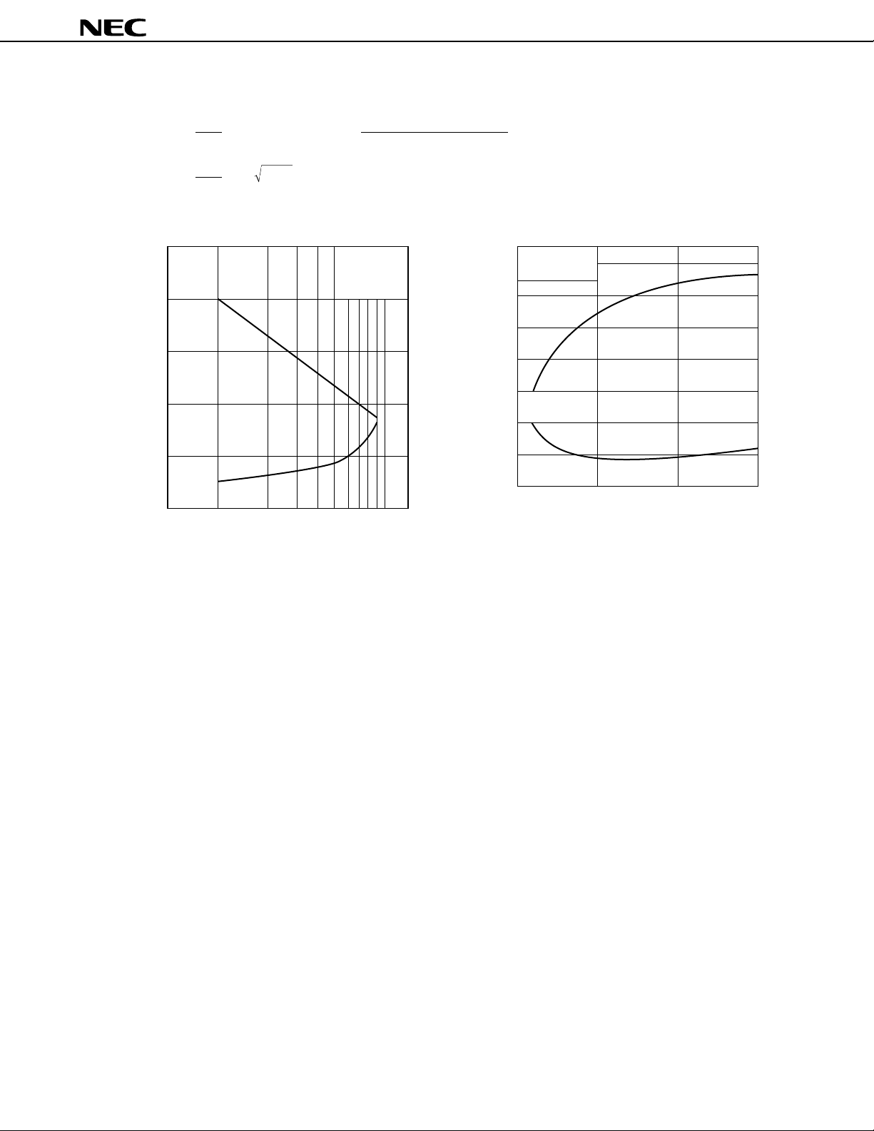
NOISE FIGURE, ASSOCIATED GAIN vs.
FREQUENCY
VDS = 2 V
I
D
= 10 mA
a
G
1.0
NF - Noise Figure - dB
0.5
NF
0
1302
4206 8 10 14
f - Frequency - GHz
222
∆
11 22
12 21
2 |S | |S |
24
20
16
2.0
1.5
12
NF - Noise Figure - dB
- Associated Gain - dB
a
G
8
1.0
0.5
4
NOISE FIGURE, ASSOCIATED GAIN vs.
DRAIN CURRENT
VDS = 2 V
f = 12 GHz
G
a
NF
ID - Drain Current - mA
14
13
12
11
10
- Associated Gain - dB
a
G
3020100
3
Page 4
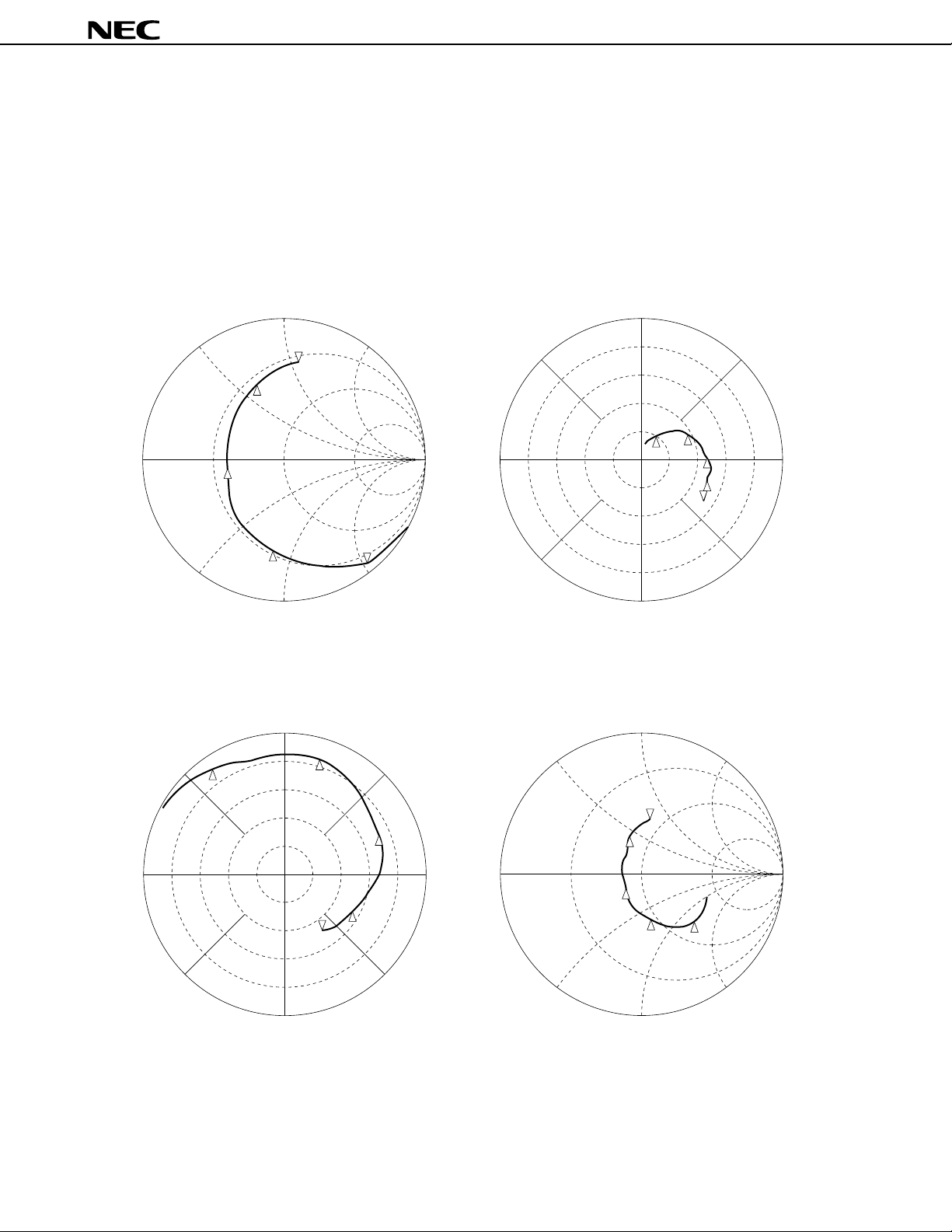
S-PARAMETERS
VDS = 2 V, ID = 10 mA
START 2 GHz, STOP 18 GHz, STEP 500 MHz
S
11
1.0
S
12
+90˚
NE325S01
Marker
4 GHz
1:
8 GHz
2:
12 GHz
3:
16 GHz
4:
18 GHz
5:
0.5 2.0
5
4
0 ∞
3
1
–0.5 –2.0
+135˚ +45˚
1
2
–1.0
S
+90˚
Rmax. = 1
21
2
+135˚
2
±180˚ 0
1
3
+45˚
4
5
–135˚ –45˚
–90˚
S
22
Rmax. = 0.25
1.0
0.5
5
2.0
4
±180˚
–135˚
–90˚
3
0
5
4
–45˚
0 ∞
–0.5
Rmax. = 5
3
4
–1.0
2
1
–2.0
Rmax. = 1
Page 5

NE325S01
S-PARAMETERS
MAG. AND ANG.
DS = 2 V, ID = 10 mA
V
FREQUENCY S11 S21 S12 S22
MHz MAG. ANG. MAG. ANG. MAG. ANG. MAG. ANG.
(deg.) (deg.) (deg.) (deg.)
2000 .999 –26.7 4.914 151.5 .029 74.5 .444 –18.9
2500 .994 –29.0 4.748 147.2 .036 73.3 .507 –26.8
3000 .952 –38.8 4.770 137.3 .044 65.3 .472 –32.7
3500 .939 –44.6 4.654 131.3 .050 62.7 .485 –37.1
4000 .926 –51.1 4.547 125.0 .055 59.3 .490 –40.9
4500 .866 –56.7 4.413 117.6 .059 53.7 .477 –45.3
5000 .821 –60.6 4.285 111.6 .064 50.8 .474 –48.5
5500 .783 –63.7 4.192 105.7 .069 48.4 .465 –51.7
6000 .788 –70.5 4.207 99.8 .075 45.1 .439 –55.4
6500 .755 –76.1 4.219 93.7 .079 41.7 .421 –58.9
7000 .721 –82.9 4.231 87.2 .085 38.6 .401 –63.4
7500 .679 –91.9 4.234 80.0 .092 33.4 .361 –69.3
8000 .634 –101.6 4.207 72.6 .095 28.8 .322 –75.7
8500 .595 –111.7 4.136 65.3 .098 24.2 .288 –83.0
9000 .563 –122.5 4.059 58.1 .104 20.5 .256 –92.1
9500 .537 –132.5 3.958 51.1 .105 16.0 .229 –101.2
10000 .505 –142.0 3.834 44.3 .108 11.7 .208 –108.5
10500 .478 –151.0 3.735 38.3 .109 8.6 .187 –114.8
11000 .451 –159.2 3.647 32.5 .110 5.3 .164 –120.0
11500 .421 –168.7 3.609 26.6 .112 1.9 .147 –124.7
12000 .415 179.9 3.589 20.6 .115 .3 .124 –133.2
12500 .424 167.1 3.556 13.4 .116 –3.3 .108 –151.1
13000 .448 152.5 3.473 5.5 .122 –7.9 .103 175.2
13500 .477 138.9 3.331 –1.8 .121 –13.1 .126 143.2
14000 .508 128.1 3.161 –8.5 .118 –15.9 .157 120.6
14500 .530 120.0 3.006 –14.2 .115 –18.0 .184 110.2
15000 .554 113.2 2.913 –19.4 .118 –18.9 .214 106.0
15500 .579 109.4 2.822 –24.6 .118 –19.9 .235 102.0
16000 .595 104.0 2.753 –30.6 .120 –22.0 .264 100.0
16500 .625 97.3 2.685 –37.0 .121 –25.5 .297 94.1
17000 .652 89.6 2.601 –43.8 .123 –30.4 .317 88.4
17500 .688 82.2 2.505 –50.8 .124 –34.2 .345 82.5
18000 .709 75.3 2.372 –57.2 .122 –37.3 .383 76.2
5
Page 6

AMP. PARAMETERS
VDS = 2 V, ID = 10 mA
NE325S01
2
FREQUENCY GUmax GAmax |S
MHz dB dB dB dB ns dB dB dB
2000 13.83 –30.68 .02 .024 .95
2500 34.12 13.53 –28.81 .05 .024 19.30 1.29
3000 24.91 13.57 –27.20 .25 .055 10.25 1.09
3500 23.80 13.36 –26.07 .27 .033 9.28 1.16
4000 22.80 13.15 –25.22 .29 .035 8.45 1.19
4500 20.04 12.89 –24.56 .48 .041 30.046 6.02 1.12
5000 18.61 12.64 –23.90 .59 .033 25.177 4.86 1.11
5500 17.63 12.45 –23.24 .67 .032 23.488 4.12 1.06
6000 17.62 12.48 –22.45 .64 .033 26.711 4.21 .93
6500 17.02 12.50 –22.08 .70 .034 25.122 3.67 .85
7000 16.47 12.53 –21.45 .73 .036 25.323 3.18 .76
7500 15.82 12.53 –20.71 .78 .040 23.957 2.68 .61
8000 15.19 12.48 –20.45 .84 .041 22.607 2.23 .48
8500 14.60 12.33 –20.15 .89 .040 21.735 1.90 .38
9000 14.12 12.17 –19.69 .91 .040 21.968 1.66 .29
9500 13.66 11.95 –19.57 .96 .039 21.196 1.48 .23
10000 13.15 15.21 11.67 –19.29 1.00 .038 20.248 1.28 .19
10500 12.73 13.86 11.45 –19.29 1.06 .033 19.297 1.13 .15
11000 12.34 13.15 11.24 –19.19 1.11 .032 18.449 .99 .12
11500 12.09 12.73 11.15 –19.05 1.15 .033 17.976 .85 .09
12000 11.99 12.61 11.10 –18.81 1.15 .033 18.424 .82 .07
12500 11.93 12.56 11.02 –18.74 1.15 .040 18.844 .86 .05
13000 11.83 12.56 10.81 –18.31 1.11 .044 19.943 .97 .05
13500 11.64 12.31 10.45 –18.38 1.12 .040 19.641 1.12 .07
14000 11.40 11.91 10.00 –18.54 1.15 .037 18.906 1.30 .11
14500 11.14 11.54 9.56 –18.76 1.19 .031 18.016 1.43 .15
15000 11.08 11.50 9.29 –18.59 1.16 .029 18.476 1.59 .20
15500 11.03 11.49 9.01 –18.57 1.14 .029 18.729 1.77 .25
16000 11.00 11.57 8.79 –18.42 1.11 .033 19.308 1.90 .31
16500 11.13 11.87 8.58 –18.33 1.07 .036 20.642 2.15 .40
17000 11.16 12.17 8.30 –18.19 1.03 .037 22.203 2.40 .46
17500 11.31 7.97 –18.10 .98 .039 25.645 2.78 .55
18000 11.22 7.50 –18.28 .99 .035 22.558 3.03 .69
21|
|S12|
2
K Delay Mason’s U G1 G2
6
Page 7

NOISE PARAMETER
<TYPICAL CONSTANT NOISE FIGURE CIRCLE>
NE325S01
1
0.6
0.2
∗
Γopt
0
0.2 0.6 1.0 2.0
0.8
1.0
2
V
DS
= 2 V
I
D
= 10 mA
f = 12 GHz
5
∞
–0.2
–0.6
–1
<NOISE PARAMETER>
DS = 2 V, ID = 10 mA
V
Freq. (GHz) NFmin. (dB) Ga (dB)
2.0 0.29 20.0 0.93 14 0.38
4.0 0.30 18.3 0.80 29 0.33
6.0 0.32 16.5 0.65 48 0.25
8.0 0.35 15.0 0.49 72 0.18
10.0 0.40 13.6 0.36 102 0.11
12.0 0.45 12.5 0.27 139 0.08
14.0 0.53 12.0 0.24 –176 0.07
16.0 0.67 11.8 0.30 –122 0.10
18.0 0.83 11.5 0.47 –58 0.22
MAG. ANG. (deg.)
Γopt.
–5
–2
Rn/50
7
Page 8

TYPICAL MOUNT PAD LAYOUT
NE325S01
2.4 mm TYP.
2.4 mm TYP.
8
Page 9

NE325S01
RECOMMENDED SOLDERING CONDITIONS
The following conditions (see table below) must be met when soldering this product.
Please consult with our sales offices in case other soldering process is used, or in case soldering is done under
different conditions.
<TYPES OF SURFACE MOUNT DEVICE>
For more details, refer to our document “SEMICONDUCTOR DEVICE MOUNTING TECHNOLOGY MANUAL”
(C10535E).
Soldering process Soldering conditions Symbol
Infrared ray reflow Peak package’s surface temperature: 230 ˚C or below, IR30-00
Reflow time: 30 seconds or below (210 ˚C or higher),
Number of reflow process: 1, Exposure limit
Partial heating method Terminal temperature: 230 ˚C or below,
Flow time: 10 seconds or below,
Exposure limit
Note
: None
Note
: None
Note Exposure limit before soldering after dry-pack package is opened.
Storage conditions: 25 ˚C and relative humidity at 65 % or less.
Caution Do not apply more than a single process at once, except for “Partial heating method”.
PRECAUTION Avoid high static voltage and electric fields, because this device is Hetero Junction field effect
transistor with shottky barrier gate.
9
Page 10

[MEMO]
NE325S01
10
Page 11

[MEMO]
NE325S01
11
Page 12

NE325S01
Caution
The Grate Care must be taken in dealing with the devices in this guide.
The reason is that the material of the devices is GaAs (Gallium Arsenide), which is
designated as harmful substance according to the law concerned.
Keep the law concerned and so on, especially in case of removal.
No part of this document may be copied or reproduced in any form or by any means without the prior written
consent of NEC Corporation. NEC Corporation assumes no responsibility for any errors which may appear in
this document.
NEC Corporation does not assume any liability for infringement of patents, copyrights or other intellectual property
rights of third parties by or arising from use of a device described herein or any other liability arising from use
of such device. No license, either express, implied or otherwise, is granted under any patents, copyrights or other
intellectual property rights of NEC Corporation or others.
While NEC Corporation has been making continuous effort to enhance the reliability of its semiconductor devices,
the possibility of defects cannot be eliminated entirely. To minimize risks of damage or injury to persons or
property arising from a defect in an NEC semiconductor device, customers must incorporate sufficient safety
measures in its design, such as redundancy, fire-containment, and anti-failure features.
NEC devices are classified into the following three quality grades:
"Standard", "Special", and "Specific". The Specific quality grade applies only to devices developed based on a
customer designated "quality assurance program" for a specific application. The recommended applications of
a device depend on its quality grade, as indicated below. Customers must check the quality grade of each device
before using it in a particular application.
Standard: Computers, office equipment, communications equipment, test and measurement equipment,
audio and visual equipment, home electronic appliances, machine tools, personal electronic
equipment and industrial robots
Special: Transportation equipment (automobiles, trains, ships, etc.), traffic control systems, anti-disaster
systems, anti-crime systems, safety equipment and medical equipment (not specifically designed
for life support)
Specific: Aircrafts, aerospace equipment, submersible repeaters, nuclear reactor control systems, life
support systems or medical equipment for life support, etc.
The quality grade of NEC devices is "Standard" unless otherwise specified in NEC's Data Sheets or Data Books.
If customers intend to use NEC devices for applications other than those specified for Standard quality grade,
they should contact an NEC sales representative in advance.
Anti-radioactive design is not implemented in this product.
M4 96.5
2
 Loading...