

Page 1
SEMICONDUCTOR TECHNICAL DATA
1
REV 3
Motorola, Inc. 1997
1/97
The MPC930/931 is a 3.3V compatible, PLL based clock driver device
targeted for high performance clock applications. With output frequencies
of up to 150MHz and output skews of 300ps the MPC930/931 is ideal for
the most demanding clock distribution designs. The device employs a
fully differential PLL design to minimize cycle to cycle and long term jitter.
This parameter is of significant importance when the clock driver is
providing the reference clock for PLL’ s on board todays microprocessors
and ASiC’s. The device offers 6 low skew outputs, and a choice between
internal or external feedback. The feedback option adds to the flexibility of
the device, providing numerous input to output frequency relationships.
• On–Board Crystal Oscillator (MPC930)
• Differential LVPECL Reference Input (MPC931)
• Fully Integrated PLL
• Output Shut Down Mode
• Output Frequency up to 150MHz
• Compatible with PowerPC and Intel Microprocessors
• 32–Lead TQFP Packaging
• Power Down Mode
• ±100ps Typical Cycle–to–Cycle Jitter
The MPC930 and MPC931 are very similar in basic functionality, but
there are some minor differences. The MPC931 has been optimized for
use as a zero delay buffer . In addition to tighter specification limits on the
phase offset of the device, a higher speed VCO has been used on the
MPC931. The MPC930, on the other hand, is more optimized for use as a
clock generator. When choosing between the 930 and 931, pay special
attention to the differences in the AC parameters of each device.
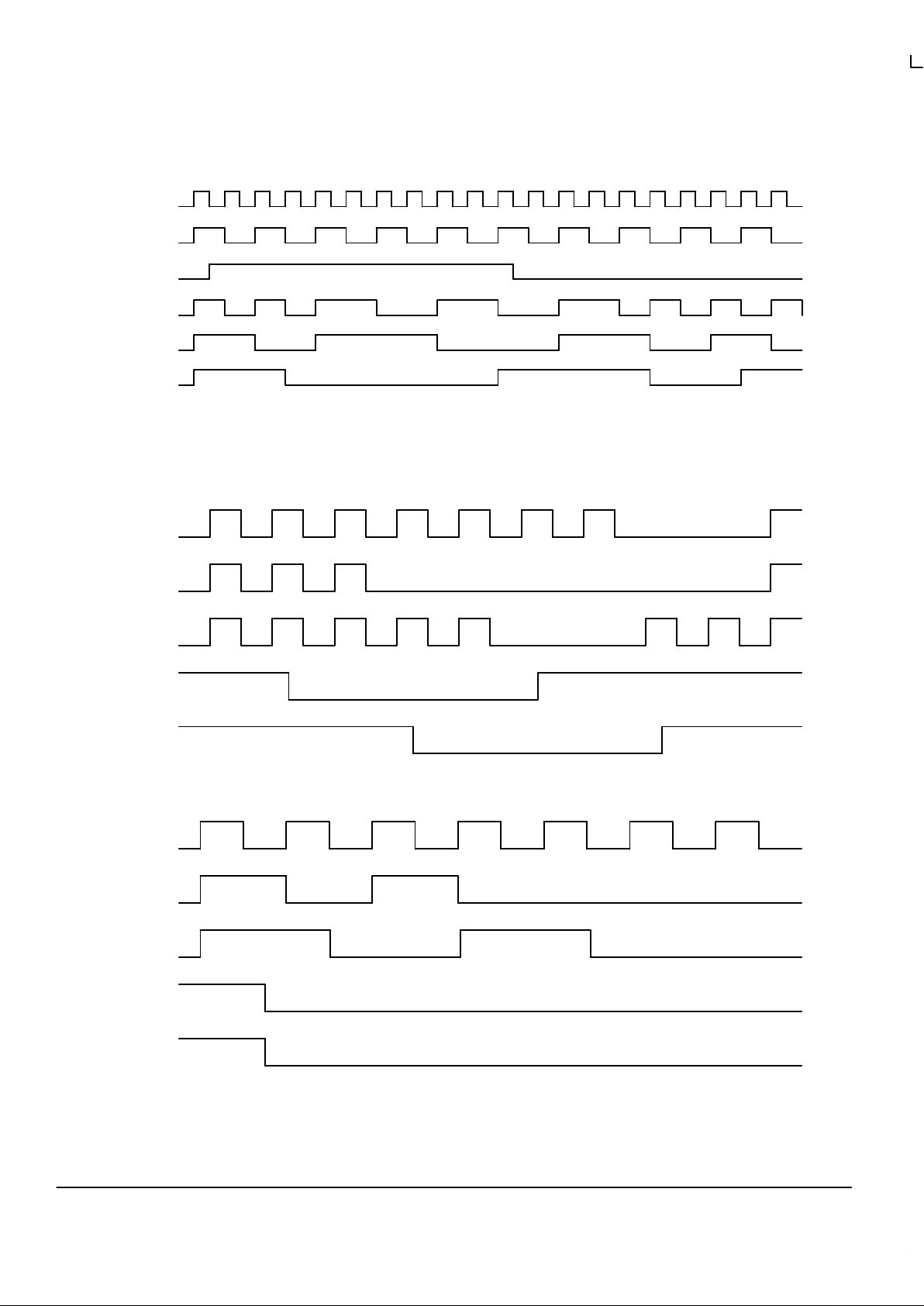
The MPC930/931 offers two power saving features for power conscious portable or “green” designs. The power down pin will
seemlessly reduce all of the clock rates by one half so that the system will run at half the potential clock rate to extend battery life.
The POWER_DN pin is synchronized internally to the slowest output clock rate. This allows the transition in and out of the
power–down mode to be output glitch free. In addition, the shut down control pins will turn off various combinations of clock
outputs while leaving a subset active to allow for total processor shut down while maintaining system monitors to “wake up” the
system when signaled. During shut down, the PLL will remain locked, if internal feedback is used, so that wake up time will be
minimized. The shut down and power down pins can be combined for the ultimate in power savings. The Shut_Dn pins are
synchronized to the clock internal to the chip to eliminate the possibility of generating runt pulses.
The MPC930/931 devices offer a great deal of flexibility in what is used as the PLL reference. The MPC930 offers an
integrated crystal oscillator that allows for an inexpensive crystal to be used as the frequency reference. For more information on
the crystal oscillator please refer to the applications section of this data sheet. In those applications where the 930/931 will be
used to regenerate clocks from an existing source or as a zero delay buffer , alternative reference clock inputs are provided. Both
devices offer an LVCMOS input that can be used as the PLL reference. In addition the MPC931 replaces the crystal oscillator
inputs with a differential PECL reference clock input that allows the device to be used in mixed technology clock distribution trees.
An internal feedback divide by 8 of the VCO frequency is compared with the input reference provided by the on–board crystal
oscillator when the internal feedback is selected. The on–board crystal oscillator requires no external components other than a
series resonant crystal (see Applications Information section for more on crystals). The internal VCO is running at 8x the input
reference clock. The outputs can be configured to run at 4x, 2x, 1.25x or 0.66x the input reference frequency. If the external
feedback is selected, one of the MPC931’s outputs must be connected to the Ext_FB pin. Using the external feedback, numerous
input/output frequency relationships can be developed.
The MPC930/931 is fully 3.3V compatible and requires no external loop filter components. All control inputs accept LVCMOS
or LVTTL compatible levels while the outputs provide LVCMOS levels with the capability to drive terminated 50Ω transmission
lines. For series terminated applications, each output can drive two 50Ω transmission lines, effectively increasing the fanout to
1:12. The device is packaged in a 32–lead TQFP package to provide the optimum combination of board density and cost.
PowerPC is a trademark of International Business Machines Corporation. Pentium is a trademark of Intel Corporation.
LOW VOLTAGE
PLL CLOCK DRIVER
FA SUFFIX
32–LEAD TQFP PACKAGE
CASE 873A–02
Page 2
MPC930 MPC931
MOTOROLA TIMING SOLUTIONS
BR1333 — Rev 6
2
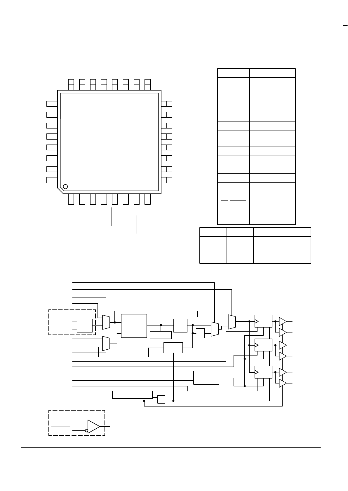
÷2÷4÷2÷4÷4
÷6
FUNCTION TABLES
TCLK_Sel Reference
0
1
xtal (PECL_CLK)
TCLK
PLL_En PLL Status
0
1
Test Mode
PLL Enabled
ExtFB_Sel Reference
0
1
Int. ÷8
Ext_FB
GNDO
Qa1
Qa0
VCCO
Div_Sela
Div_Selb
Div_Selc
NC
GNDO
Qc1
Qc0
VCCO
Ext_FB
Shut_Dn1
Shut_Dn0
NC
GNDO
Qb0
Qb1
VCCO
ExtFB_Sel
TCLK_Sel
PLL_En
NC
NC
PLL_VCC
Power_Dn
TCLK
MR/Tristate
xtal1 (930)
xtal2 (930)
GNDI
25
26
27
28
29
30
31
32
15
14
13
12
11
10
9
12345678
24 23 22 21 20 19 18 17
16
MPC930/
MPC931
Power_Dn PLL Status
0
1
VCO/1
VCO/2
Div_Sela,b,c
0
1
Qa Qb Qc
Shut_Dn1
0
0
1
1
Div_Seln
Qb & Qc Low, Qa Toggle
Qa & Qb Low, Qc Toggle
Qb Low, Qa & Qc Toggle
All Toggle
Shut_Dn0
0
1
0
1
Figure 1. 32–Lead Pinout (Top View)
PECL_CLK (931)
PECL_CLK (931)
Figure 2. Logic Diagram
POWER–ON RESET
VCO
PHASE
DETECTOR
LPF
÷
8
MR/Tristate
xtal
OSC
Shut_Dn1
Shut_Dn0
xtal2
xtal1
PLL_En
Qa0
Qb0
Qb1
Power_Dn
÷2/÷
4
÷2/÷
4
÷4/÷
6
Qc0
Qc1
DISABLE
LOGIC
Div_Selb
Div_Sela
Qa1
TCLK
TCLK_Sel
Ext_FB
ExtFB_Sel
Div_Selc
MPC930
PECL_CLK
PECL_CLK
MPC931
MR/Tristate PLL Status
0
1
Disabled
Enabled
(Pullup)
(Pullup)
(Pulldown)
(Pullup)
(Pullup)
(Pulldown)
(Pulldown)
(Pulldown)
(Pullup)
(Pullup)
(Pulldown)
(Pullup)
(Pullup)
(None)
÷
2
Page 3
MPC930 MPC931
TIMING SOLUTIONS
BR1333 — Rev 6
3 MOTOROLA
Figure 3. Power_Dn Timing Diagram
VCO
Figure 4. Shut_Dn Timing Diagram
Qa
Qb
Qc
SHUT_DN0
SHUT_DN1
Qa (÷2)
Qb (÷4)
Qc (
÷
6)
SHUT_DN0
SHUT_DN1
VCO/2
Power_Dn
Qa (÷2)
Qb (÷4)
Qc (÷6)
Page 4
MPC930 MPC931
MOTOROLA TIMING SOLUTIONS
BR1333 — Rev 6
4
ABSOLUTE MAXIMUM RATINGS*
Symbol Parameter Min Max Unit
V
CC
Supply Voltage –0.3 4.6 V
V
I
Input Voltage –0.3 VDD + 0.3 V
I
IN
Input Current ±20 mA
T
Stor
Storage Temperature Range –40 125 °C
* Absolute maximum continuous ratings are those values beyond which damage to the device may occur. Exposure to these conditions or
conditions beyond those indicated may adversely affect device reliability. Functional operation under absolute–maximum–rated conditions is
not implied.
PLL INPUT REFERENCE CHARACTERISTICS (TA = 0 to 70°C)
Symbol Characteristic Min Max Unit Condition
tr, t
f
TCLK Input Rise/Falls 3.0 ns
f
ref
Reference Input Frequency 10 Note 1. MHz
f
refDC
Reference Input Duty Cycle 25 75 %
1. Maximum input reference frequency is limited by the VCO lock range and the feedback divider.
DC CHARACTERISTICS (TA = 0° to 70°C, VCC = 3.3V ±5%)
Symbol Characteristic Min Typ Max Unit Condition
V
IH
Input HIGH Voltage 2.0 3.6 V
V
IL
Input LOW Voltage 0.8 V
V
OH
Output HIGH Voltage 2.4 V IOH = –20mA (Note 2.)
V
OL
Output LOW Voltage 0.5 V IOL = 20mA (Note 2.)
I
IN
Input Current ±120 µA Note 3.
I
CC
Maximum Core Supply Current 65 85 mA
I
CCPLL
Maximum PLL Supply Current 15 20 mA
C
IN
4 pF
C
pd
25 pF Per Output
2. The MPC930/931 outputs can drive series or parallel terminated 50Ω (or 50Ω to VCC/2) transmission lines on the incident edge (see Applications
Info section).
3. Inputs have pull–up/pull–down resistors which affect input current.
Page 5
MPC930 MPC931
TIMING SOLUTIONS
BR1333 — Rev 6
5 MOTOROLA
MPC930 AC CHARACTERISTICS (TA = 0° to 70°C, VCC = 3.3V ±5%)
Symbol Characteristic Min Typ Max Unit Condition
f
xtal
Crystal Oscillator Frequency Range 10 20 MHz Note 5., Note 7.
f
ref
Input Reference Frequency Note 7. Note 7. MHz Ref = TCLK
t
os
Output–to–Output Skew Same Frequency
(Note 4.) Diff Frequency
Same Frequency
Diff Frequency
200
300
300
450
300
400
400
600
ps f
max
≤ 100MHz
f
max
≤ 100MHz
f
max
> 100MHz
f
max
> 100MHz
f
VCO
VCO Lock Range Power_Dn = 0
Power_Dn = 1
100
50
280
140
MHz
f
max
Maximum Output Frequency Qa, Qb (÷2)
Qa, Qb, Qc (÷4)
Qc (÷6)
140
80
47
MHz Note 4.
t
pd
TCLK to EXT_FB Delay –600 –100 400 ps f
ref
= 50MHz, FB = ÷4
t
pw
Output Duty Cycle (Note 4.) t
CYCLE
/2
–750
t
CYCLE
/2
±500
t
CYCLE
/2
+750
ps
tr, t
f
Output Rise/Fall Time (Note 4.) 0.1 1.0 ns 0.8 to 2.0V
t
PLZ
, t
PHZ
Output Disable Time 2.0 8.0 ns 50Ω to VCC/2
t
PZL
Output Enable Time 2.0 10 ns 50Ω to VCC/2
t
jitter
Cycle–to–Cycle Jitter (Peak–to–Peak) ±100 ps Note 6.
t
lock
Maximum PLL Lock Time 10 ms
4. Measured with 50Ω to VCC/2 termination.
5. See Applications Info section for more Crystal specifications.
6. See Applications Info section for more jitter information.
7. Input reference frequency is bounded by VCO lock range and feedback divide selection.
MPC931 AC CHARACTERISTICS (TA = 0° to 70°C, VCC = 3.3V ±5%)
Symbol Characteristic Min Typ Max Unit Condition
f
ref
Input Reference Frequency Note 11. Note 11. MHz
t
os
Output–to–Output Skew Same Frequency
(Note 8.) Diff Frequency
Same Frequency
Diff Frequency
200
300
300
450
300
400
400
600
ps f
max
≤ 100MHz
f
max
≤ 100MHz
f
max
> 100MHz
f
max
> 100MHz
f
VCO
VCO Lock Range Power_Dn = 0
Power_Dn = 1
200
100
480
240
MHz
f
max
Maximum Output Frequency Qa, Qb (÷2)
Qa, Qb, Qc (÷4)
Qc (÷6)
150
120
80
MHz Note 9.
t
pd
Reference to EXT_FB Average Delay TCLK
PECL_CLK
–150
–400
0
–250
+150
–100
ps f
ref
= 50MHz; FB = ÷8;
Note 12.
t
pw
Output Duty Cycle (Note 8.) t
CYCLE
/2
–750
t
CYCLE
/2
±500
t
CYCLE
/2
+750
ps
tr, t
f
Output Rise/Fall Time (Note 8.) 0.1 1.0 ns 0.8 to 2.0V
t
PLZ
, t
PHZ
Output Disable Time 2.0 8.0 ns 50Ω to VCC/2
t
PZL
Output Enable Time 2.0 10 ns 50Ω to VCC/2
t
jitter
Cycle–to–Cycle Jitter (Peak–to–Peak) ±100 ps Note 10.
t
lock
Maximum PLL Lock Time 10 ms
8. Measured with 50Ω to VCC/2 termination.
9. f
max
limited by skew spec. Outputs will generate valid CMOS signals up to 180MHz.
10.See Applications Info section for more jitter information.
11.Input reference frequency is bounded by VCO lock range and feedback divide selection.
12.tpd is specified for 50MHz input reference, the window will shrink/grow proportionally from the minimum limit with shorter/linger reference
periods. The tpd does not include jitter.
Page 6

MPC930 MPC931
MOTOROLA TIMING SOLUTIONS
BR1333 — Rev 6
6
APPLICATIONS INFORMATION
Programming the MPC930/931
The MPC930/931 clock driver outputs can be configured
into several frequency relationships, in addition the external
feedback option allows for a great deal of flexibility in
establishing unique input to output frequency relationships.
The output dividers for the three output groups allows the
user to configure the outputs into 1:1, 2:1, 3:1, 3:2 and 3:2:1
frequency ratios. The use of even dividers ensures that the
output duty cycle is always 50%. Table 1 illustrates the
various output configurations, the table describes the outputs
using the VCO frequency as a reference. As an example for a
3:2:1 relationship the Qa outputs would be set at VCO/2, the
Qb’s at VCO/4 and the Qc’s at VCO/6. These settings will
provide output frequencies with a 3:2:1 relationship.
The division settings establish the output relationship, but
one must still ensure that the VCO will be stable given the
frequency of the outputs desired. The VCO lock range can be
found in the specification tables. The feedback frequency
and the Power_Dn pin can be used to situate the VCO into a
frequency range in which the PLL will be stable. The design
of the PLL is such that for output frequencies between 25 and
180MHz the MPC930/931 can generally be configured into a
stable region.
The relationship between the input reference and the
output frequency is also very flexible. Table 2 shows the
multiplication factors between the inputs and outputs when
the internal feedback option is used. For external feedback
Table 1 can be used to determine the multiplication factor,
there are too many potential combinations to tabularize the
external feedback condition. Figure 5 through Figure 10
illustrates several programming possibilities, although not
exhaustive it is representative of the potential applications.
Table 1. Programmable Output Frequency Relationships
(Power_Dn = ‘0’)
INPUTS OUTPUTS
Div_Sela Div_Selb Div_Selc Qa Qb Qc
0 0 0 VCO/2 VCO/2 VCO/4
0 0 1 VCO/2 VCO/2 VCO/6
0 1 0 VCO/2 VCO/4 VCO/4
0 1 1 VCO/2 VCO/4 VCO/6
1 0 0 VCO/4 VCO/2 VCO/4
1 0 1 VCO/4 VCO/2 VCO/6
1 1 0 VCO/4 VCO/4 VCO/4
1 1 1 VCO/4 VCO/4 VCO/6
Table 2. Input Reference/Output Frequency Relationships (Internal Feedback Only)
INPUTS OUTPUTS
Qa Qb Qc
Div_Sela Div_Selb Div_Selc Power_Dn=0 Power_Dn=1 Power_Dn=0 Power_Dn=1 Power_Dn=0 Power_Dn=1
0 0 0 4x 2x 4x 2x 2x x
0 0 1 4x 2x 4x 2x 4/3x 2/3x
0 1 0 4x 2x 2x x 2x x
0 1 1 4x 2x 2x x 4/3x 2/3x
1 0 0 2x x 4x 2x 2x x
1 0 1 2x x 4x 2x 4/3x 2/3x
1 1 0 2x x 2x x 2x x
1 1 1 2x x 2x x 4/3x 2/3x
Page 7

MPC930 MPC931
TIMING SOLUTIONS
BR1333 — Rev 6
7 MOTOROLA
MPC930
Figure 5. Dual Frequency Configuration
Div_Sela‘0’
Div_Selb‘1’
Div_Selc‘0’
ExtFB_Sel‘0’
Input Ref16.66MHz
66.66MHz (Processor)Qa
33.33MHz (PCI)Qb
33.33MHz (PCI)Qc
2
2
2
MPC930
Figure 6. Single Frequency Configuration
Div_Sela‘1’
Div_Selb‘1’
Div_Selc‘0’
ExtFB_Sel‘0’
Input Ref16.66MHz
33.33MHzQa
33.33MHzQb
33.33MHzQc
2
2
2
MPC931
Figure 7. “Zero” Delay Fractional Multiplier
Div_Sela‘1’
Div_Selb‘1’
Div_Selc‘1’
ExtFB_Sel‘1’
Input Ref33.33MHz
50MHzQa
50MHzQb
33.33MHzQc
2
2
2
Figure 8. “Zero” Delay Fractional Divider
Ext_FB
1
MPC931
Div_Sela‘0’
Div_Selb‘1’
Div_Selc‘1’
ExtFB_Sel‘1’
Input Ref50MHz
100MHzQa
50MHzQb
33.33MHzQc
2
2
2
Ext_FB
1
MPC931
Figure 9. “Zero” Delay Multiply by 3 (50% Duty Cycle)
Div_Sela‘0’
Div_Selb‘0’
Div_Selc‘1’
ExtFB_Sel‘1’
Input Ref33.33MHz
100MHzQa
100MHzQb
33.33MHzQc
2
2
2
Figure 10. “Zero” Delay Divide by 3 (50% Duty Cycle)
Ext_FB
1
MPC931
Div_Sela‘0’
Div_Selb‘0’
Div_Selc‘1’
ExtFB_Sel‘1’
Input Ref100MHz
100MHzQa
100MHzQb
33.33MHzQc
2
2
2
Ext_FB
1
Using the MPC930/931 as a Zero Delay Buffer
The external feedback option of the MPC930/931 clock
driver allows for its use as a zero delay buffer . By using one of
the outputs as a feedback to the PLL the propagation delay
through the device is eliminated. The PLL works to align the
output edge with the input reference edge thus producing a
near zero delay. The Tpd of the device is specified in the
specification tables. For zero delay buffer applications, the
MPC931 is recommended over the MPC930. The MPC931
has been optimized and specified specifically for use as a
zero delay buffer.
When used as a zero delay buffer the MPC930/931 will
likely be in a nested clock tree application. For these
applications the MPC931 offers a LVPECL clock input as a
PLL reference. This allows the user to use LVPECL as the
primary clock distribution device to take advantage of its far
superior skew performance. The MPC931 then can lock onto
the LVPECL reference and translate with near zero delay to
low skew LVCMOS outputs. Clock trees implemented in this
fashion will show significantly tighter skews than trees
developed from CMOS fanout buffers.
To minimize part–to–part skew the external feedback
option again should be used. The PLL in the MPC931
decouples the delay of the device from the propagation delay
variations of the internal gates. From the specification table
one sees a Tpd variation of only ±150ps, thus for multiple
devices under identical configurations the part–to–part skew
will be around 850ps (300ps for Tpd variation plus 300ps
Page 8

MPC930 MPC931
MOTOROLA TIMING SOLUTIONS
BR1333 — Rev 6
8
output–to–output skew plus 250ps jitter). For devices that are
configured differently the differences between the nominal
delays must also be accounted for.
When using the MPC931 as a zero delay buffer there is
more information which can help minimize the overall timing
uncertainty. To fully minimize the specified uncertainty, it is
crucial that the relative position of the outputs be known. It is
recommended that if all of the outputs are going to be used
that the Qc0 output be used as the feedback reference. The
Qc0 output lies in the middle of the other outputs with respect
to output skew. Therefore it can be assumed that the output
to output skew of the device is ±150ps with respect to output
Qc0.
There will be some cases where only a subset of the
outputs of the MPC931 are required. There is significantly
tighter skew performance between outputs on a common
bank (i.e., Qa0 to Qa1). The skews between these common
bank outputs are outlined in the table below. In general the
skews between outputs on a given bank is about a third of the
skew between all banks, reducing the skew to a value of
100ps.
Table 3. Within–Bank Skews
Outputs Relative Skews
Qa0 → Qa1 +35ps, ±50ps
Qb0 → Qb1 –30ps, ±50ps
Qc0 → Qc1 20ps, ±50ps
Jitter Performance of the MPC930/931
With the clock rates of today’s digital systems continuing
to increase more emphasis is being placed on clock
distribution design and management. Among the issues
being addressed is system clock jitter and how that affects
the overall system timing budget. The MPC930/931 was
designed to minimize clock jitter by employing a differential
bipolar PLL as well as incorporating numerous power and
ground pins in the design. The following few paragraphs will
outline the jitter performance of the MPC930/931, illustrate
the measurement limitations and provide guidelines to
minimize the jitter of the device.
The most commonly specified jitter parameter is
cycle–to–cycle jitter. Unfortunately with today’s high
performance measurement equipment there is no way to
measure this parameter for jitter performance in the class
demonstrated by the MPC930/931. As a result different
methods are used which approximate cycle–to–cycle jitter.
The typical method of measuring the jitter is to accumulate a
large number of cycles, create a histogram of the edge
placements and record peak–to–peak as well as standard
deviations of the jitter. Care must be taken that the measured
edge is the edge immediately following the trigger edge. If
this is not the case the measurement inaccuracy will add
significantly to the measured jitter. The oscilloscope cannot
collect adjacent pulses, rather it collects data from a very
large sample of pulses. It is safe to assume that collecting
pulse information in this mode will produce jitter values
somewhat larger than if consecutive cycles were measured,
therefore, this measurement will represent an upper bound of
cycle–to–cycle jitter. Most likely, this is a conservative
estimate of the cycle–to–cycle jitter.
1212
12
Peak–to–Peak PLL Jitter
Peak–to–Peak Period Jitter
Figure 11. PLL Jitter and Edge Displacement
1232
12
123
3
Peak–to–Peak PLL Jitter
Peak–to–Peak Period Jitter
There are two sources of jitter in a PLL based clock driver,
the commonly known random jitter of the PLL and the less
intuitive jitter caused by synchronous, different frequency
outputs switching. For the case where all of the outputs are
switching at the same frequency the total jitter is exactly
equal to the PLL jitter. In a device, like the MPC930/931,
where a number of the outputs can be switching
synchronously but at different frequencies a “multi–modal”
jitter distribution can be seen on the highest frequency
outputs. Because the output being monitored is affected by
the activity on the other outputs it is important to consider
what is happening on those other outputs. From Figure 11,
one can see for each rising edge on the higher frequency
signal the activity on the lower frequency signal is not
constant. The activity on the other outputs tends to alter the
internal thresholds of the device such that the placement of
the edge being monitored is displaced in time. Because the
signals are synchronous the relationship is periodic and the
resulting jitter is a compilation of the PLL jitter superimposed
on the displaced edges. When histograms are plotted the
jitter looks like a “multi–modal” distribution as pictured in
Figure 11 on page 8. Depending on the size of the PLL jitter
and the relative displacement of the edges the “multi–modal”
distribution will appear truly “multi–modal” or simply like a
“fat” Gaussian distribution. Again note that in the case where
Page 9

MPC930 MPC931
TIMING SOLUTIONS
BR1333 — Rev 6
9 MOTOROLA
all the outputs are switching at the same frequency there is
no edge displacement and the jitter is reduced to that of
the PLL.
Figure 12 graphically represents the PLL jitter of the
MPC930/931. The data was taken for several different output
configurations. Because of the relatively few outputs on the
MPC930/931, the multimodal distribution is of a second order
affect on the 930/931 and can be ignored. As one can see in
the figure the PLL jitter is much less dependent on output
configuration than on internal VCO frequency . However , for a
given VCO frequency, a lower output frequency produces
more jitter.
Figure 12. RMS Jitter versus VCO Frequency
(Qa0 Output)
10
15
20
25
30
35
40
45
80 120 160 200 240 280
Conf 1
Conf 2
Conf 1 = Qa=÷2, Qb=Qc=÷4
Conf 2 = Qa=
÷
2, Qb=Qc=Shut Down
Conf 3 = Qa=
÷
4, Qb=Qc=Shut Down
VCO Frequency (MHz)
RMS Jitter (ps)
Figure 13. RMS Jitter versus Output Frequency
(Qa0 Output)
10
15
20
25
30
35
20 40 60 80 100 120 140
Frequency Output (MHz)
RMS Jitter (ps)
Conf 2 = Qa=÷2, Qb=Qc=Shut Down
Conf 3 = Qa=
÷
4, Qb=Qc=Shut Down
Conf 3
Conf 2
Conf 3
Finally from the data there are some general guidelines
that, if followed, will minimize the output jitter of the device.
First and foremost always configure the device such that the
VCO runs as fast as possible. This is by far the most critical
parameter in minimizing jitter. Second keep the reference
frequency as high as possible. More frequent updates at the
phase detector will help to reduce jitter. Note that if there is a
tradeoff between higher reference frequencies and higher
VCO frequency always chose the higher VCO frequency to
minimize jitter. The third guideline is to try to shut down
outputs that are unused. Minimizing the number of switching
outputs will minimize output jitter.
Power Supply Filtering
The MPC930/931 is a mixed analog/digital product and as
such it exhibits some sensitivities that would not necessarily
be seen on a fully digital product. Analog circuitry is naturally
susceptible to random noise, especially if this noise is seen
on the power supply pins. The MPC930/931 provides
separate power supplies for the output buffers (V
CCO
) and
the internal PLL (PLL_VCC) of the device. The purpose of
this design technique is to try and isolate the high switching
noise digital outputs from the relatively sensitive internal
analog phase–locked loop. In a controlled environment such
as an evaluation board this level of isolation is sufficient.
However, in a digital system environment where it is more
difficult to minimize noise on the power supplies a second
level of isolation may be required. The simplest form of
isolation is a power supply filter on the PLL_VCC pin for the
MPC930/931.
Figure 14. Power Supply Filter
PLL_VCC
VCC
MPC930/931
0.01µF
22
µ
F
0.01
µ
F
3.3V
RS=10–15
Ω
Figure 14 illustrates a typical power supply filter scheme.
The MPC930/931 is most susceptible to noise with spectral
content in the 1KHz to 1MHz range. Therefore the filter
should be designed to target this range. The key parameter
that needs to be met in the final filter design is the DC voltage
drop that will be seen between the VCC supply and the
PLL_VCC pin of the MPC930/931. From the data sheet the
I
PLL_VCC
current (the current sourced through the PLL_VCC
pin) is typically 15mA (20mA maximum), assuming that a
minimum of 3.0V must be maintained on the PLL_VCC pin
very little DC voltage drop can be tolerated when a 3.3V V
CC
supply is used. The resistor shown in Figure 14 must have a
resistance of 10–15Ω to meet the voltage drop criteria. The
RC filter pictured will provide a broadband filter with
approximately 100:1 attenuation for noise whose spectral
content is above 20KHz. As the noise frequency crosses the
series resonant point of an individual capacitor it’s overall
impedance begins to look inductive and thus increases with
increasing frequency. The parallel capacitor combination
shown ensures that a low impedance path to ground exists
for frequencies well above the bandwidth of the PLL.
Page 10

MPC930 MPC931
MOTOROLA TIMING SOLUTIONS
BR1333 — Rev 6
10
Although the MPC930/931 has several design features to
minimize the susceptibility to power supply noise (isolated
power and grounds and fully differential PLL) there still may
be applications in which overall performance is being
degraded due to system power supply noise. The power
supply filter schemes discussed in this section should be
adequate to eliminate power supply noise related problems
in most designs.
Using the Power Management Features of the
MPC930/931
The MPC930/931 clock driver offers two different features
that designers can take advantage of for managing power
dissipation in their designs. The first feature allows the user
to turn off outputs which drive portions of the system which
may go idle in a sleep mode. The Shut_Dn pins allow for
three different combinations of output shut down schemes.
The schemes are summarized in the function tables in the
data sheet. The MPC930/931 synchronizes the shut down
signals internal to the chip and applies them in a manner
which eliminates the possibility of creating runt pulse on the
outputs. The device waits for the output to go into the “LOW”
state prior to disabling. When the outputs are re–enabled the
device waits and re–enables the output such that the
transition is synchronous and in the proper phase
relationship to the outputs which remained active.
The Power_Dn pin offers another means of implementing
power management schemes into a design. To use this
feature the device must be set up in its normal operating
mode with the Power_Dn pin “LOW”, in addition the user
must use the internal feedback option. If the external
feedback option were used the output frequency reduction
would change the feedback frequency and the PLL will lose
lock. When the Power_Dn pin is driven “HIGH” the
MPC930/931 synchronizes the signal to the internal clock
and then seemlessly reduces the frequency of the outputs by
one half. The Power_Dn signal is synchronized to the
slowest internal VCO clock. It waits until both VCO clocks are
in the “LOW” state and then switches from the nominal speed
VCO clock to the half speed VCO clock. This will in turn
cause the current output pulse to stretch to reflect the
reduction in output frequency. When the Power_Dn pin is
brought back “LOW” the device will again wait until both of
the VCO clocks are “LOW” and then switch to the nominal
VCO clock. This will cause the current output pulses, and all
successive pulses, to shrink to match the higher output
frequency. Both the power up and power down features are
illustrated in the timing diagrams of in this data sheet.
Timing diagrams for both of the power management
features are shown in Figure 3 and Figure 4 on page 3.
Using the On–Board Crystal Oscillator
The MPC930 features an on–board crystal oscillator to
allow for seed clock generation as well as final distribution.
The on–board oscillator is completely self contained so that
the only external component required is the crystal. As the
oscillator is somewhat sensitive to loading on its inputs the
user is advised to mount the crystal as close to the
MPC930/931 as possible to avoid any board level parasitics.
To facilitate co–location surface mount crystals are
recommended, but not required.
The oscillator circuit is a series resonant circuit as
opposed to the more common parallel resonant circuit, this
eliminates the need for large on–board capacitors. Because
the design is a series resonant design for the optimum
frequency accuracy a series resonant crystal should be used
(see specification table below). Unfortunately most off the
shelf crystals are characterized in a parallel resonant mode.
However a parallel resonant crystal is physically no different
than a series resonant crystal, a parallel resonant crystal is
simply a crystal which has been characterized in its parallel
resonant mode. Therefore in the majority of cases a parallel
specified crystal can be used with the MPC930 with just a
minor frequency error due to the actual series resonant
frequency of the parallel resonant specified crystal. Typically
a parallel specified crystal used in a series resonant mode
will exhibit an oscillatory frequency a few hundred ppm lower
than the specified value. For most processor implement–
ations a few hundred ppm translates into kHz inaccuracies, a
level which does not represent a major issue.
Table 4. Crystal Specifications
Parameter Value
Crystal Cut Fundamental AT Cut
Resonance Series Resonance*
Frequency Tolerance ±75ppm at 25°C
Frequency/Temperature Stability ±150pm 0 to 70°C
Operating Range 0 to 70°C
Shunt Capacitance 5–7pF
Equivalent Series Resistance (ESR) 50 to 80Ω Max
Correlation Drive Level 100µW
Aging 5ppm/Yr (First 3 Y ears)
* See accompanying text for series versus parallel resonant
discussion.
The MPC930 is a clock driver which was designed to
generate outputs with programmable frequency relationships
and not a synthesizer with a fixed input frequency. As a result
the crystal input frequency is a function of the desired output
frequency. For a design which utilizes the external feedback
to the PLL the selection of the crystal frequency is straight
forward; simply chose a crystal which is equal in frequency to
the fed back signal. To determine the crystal required to
produce the desired output frequency for an application
which utilizes internal feedback the block diagram of
Figure 15 should be used. The P and the M values for the
MPC930/931 are also included in Figure 15. The M values
can be found in the configuration tables included in this
applications section.
Page 11

MPC930 MPC931
TIMING SOLUTIONS
BR1333 — Rev 6
11 MOTOROLA
Figure 15. PLL Block Diagram
f
ref
Phase
Detector
QnVCO
LPF
÷
P
÷
N
÷
m
N
f
ref
+
fQn · N · P
m
f
ref
+
f
VCO
m
,f
VCO
+
fQn·N·P
m = 8
P = 1 (Power_Dn=‘0’), 2 (Power_Dn=‘1’)
For the MPC930 clock driver, the following will provide an
example of how to determine the crystal frequency required
for a given design.
Given:
Qa = 66.6MHz
Qb = 33.3MHz
Qc = 22.2MHz
Power_Dn = ‘0’
f
ref
+
fQn · N · P
m
From Table 4
fQc = VCO/6 then N = 6
From Figure 15
m = 8 and P = 1
f
ref
+
22.22 · 6 · 1
8
+
16.66MHz
Driving Transmission Lines
The MPC930/931 clock driver was designed to drive high
speed signals in a terminated transmission line environment.
To provide the optimum flexibility to the user the output
drivers were designed to exhibit the lowest impedance
possible. With an output impedance of less than 10Ω the
drivers can drive either parallel or series terminated
transmission lines. For more information on transmission
lines the reader is referred to application note AN1091 in the
Timing Solutions brochure (BR1333/D).
In most high performance clock networks point–to–point
distribution of signals is the method of choice. In a
point–to–point scheme either series terminated or parallel
terminated transmission lines can be used. The parallel
technique terminates the signal at the end of the line with a
50Ω resistance to VCC/2. This technique draws a fairly high
level of DC current and thus only a single terminated line can
be driven by each output of the MPC930/931 clock driver. For
the series terminated case however there is no DC current
draw, thus the outputs can drive multiple series terminated
lines. Figure 16 illustrates an output driving a single series
terminated line vs two series terminated lines in parallel.
When taken to its extreme the fanout of the MPC930/931
clock driver is effectively doubled due to its capability to drive
multiple lines.
Figure 16. Single versus Dual Transmission Lines
7
Ω
IN
MPC930/931
OUTPUT
BUFFER
RS = 43
Ω
ZO = 50
Ω
OutA
7
Ω
IN
MPC930/931
OUTPUT
BUFFER
RS = 43
Ω
ZO = 50
Ω
OutB0
RS = 43
Ω
ZO = 50
Ω
OutB1
The waveform plots of Figure 17 show the simulation
results of an output driving a single line vs two lines. In both
cases the drive capability of the MPC930/931 output buffers
is more than sufficient to drive 50Ω transmission lines on the
incident edge. Note from the delay measurements in the
simulations a delta of only 43ps exists between the two
differently loaded outputs. This suggests that the dual line
driving need not be used exclusively to maintain the tight
output–to–output skew of the MPC930/931. The output
waveform in Figure 17 shows a step in the waveform, this
step is caused by the impedance mismatch seen looking into
the driver. The parallel combination of the 43Ω series resistor
plus the output impedance does not match the parallel
combination of the line impedances. The voltage wave
launched down the two lines will equal:
VL = VS ( Zo / (Rs + Ro +Zo))
Zo = 50Ω || 50Ω
Rs = 43Ω || 43Ω
Ro = 7Ω
VL = 3.0 (25 / (21.5 + 7 + 25) = 3.0 (25 / 53.5)
= 1.40V
At the load end the voltage will double, due to the near
unity reflection coefficient, to 2.8V. It will then increment
towards the quiescent 3.0V in steps separated by one round
trip delay (in this case 4.0ns).
Page 12

MPC930 MPC931
MOTOROLA TIMING SOLUTIONS
BR1333 — Rev 6
12
Figure 17. Single versus Dual Waveforms
TIME (nS)
VOLTAGE (V)
3.0
2.5
2.0
1.5
1.0
0.5
0
2 4 6 8 10 12 14
OutB
tD = 3.9386
OutA
tD = 3.8956
In
Since this step is well above the threshold region it will not
cause any false clock triggering, however designers may be
uncomfortable with unwanted reflections on the line. To
better match the impedances when driving multiple lines the
situation in Figure 18 should be used. In this case the series
terminating resistors are reduced such that when the parallel
combination is added to the output buffer impedance the line
impedance is perfectly matched.
Figure 18. Optimized Dual Line Termination
7
Ω
MPC930/931
OUTPUT
BUFFER
RS = 36
Ω
ZO = 50
Ω
RS = 36
Ω
ZO = 50
Ω
7Ω + 36Ω k 36Ω = 50Ω k 50Ω
25Ω = 25Ω
SPICE level output buffer models are available for
engineers who want to simulate their specific interconnect
schemes. In addition IV characteristics are in the process of
being generated to support the other board level simulators in
general use.
Page 13

MPC930 MPC931
TIMING SOLUTIONS
BR1333 — Rev 6
13 MOTOROLA
OUTLINE DIMENSIONS
FA SUFFIX
TQFP PACKAGE
CASE 873A–02
ISSUE A
DETAIL Y
A
S1
VB
1
8
9
17
25
32
AE
AE
P
DETAIL Y
BASE
N
J
DF
METAL
SECTION AE–AE
G
SEATING
PLANE
R
Q
_
W
K
X
0.250 (0.010)
GAUGE PLANE
E
C
H
DETAIL AD
NOTES:
1. DIMENSIONING AND TOLERANCING PER ANSI
Y14.5M, 1982.
2. CONTROLLING DIMENSION: MILLIMETER.
3. DATUM PLANE –AB– IS LOCATED AT BOTTOM OF
LEAD AND IS COINCIDENT WITH THE LEAD
WHERE THE LEAD EXITS THE PLASTIC BODY AT
THE BOTTOM OF THE PARTING LINE.
4. DATUMS –T–, –U–, AND –Z– TO BE DETERMINED
AT DATUM PLANE –AB–.
5. DIMENSIONS S AND V TO BE DETERMINED AT
SEATING PLANE –AC–.
6. DIMENSIONS A AND B DO NOT INCLUDE MOLD
PROTRUSION. ALLOWABLE PROTRUSION IS
0.250 (0.010) PER SIDE. DIMENSIONS A AND B
DO INCLUDE MOLD MISMATCH AND ARE
DETERMINED AT DATUM PLANE –AB–.
7. DIMENSION D DOES NOT INCLUDE DAMBAR
PROTRUSION. DAMBAR PROTRUSION SHALL
NOT CAUSE THE D DIMENSION TO EXCEED
0.520 (0.020).
8. MINIMUM SOLDER PLATE THICKNESS SHALL BE
0.0076 (0.0003).
9. EXACT SHAPE OF EACH CORNER MAY VARY
FROM DEPICTION.
DIMAMIN MAX MIN MAX
INCHES
7.000 BSC 0.276 BSC
MILLIMETERS
B 7.000 BSC 0.276 BSC
C 1.400 1.600 0.055 0.063
D 0.300 0.450 0.012 0.018
E 1.350 1.450 0.053 0.057
F 0.300 0.400 0.012 0.016
G 0.800 BSC 0.031 BSC
H 0.050 0.150 0.002 0.006
J 0.090 0.200 0.004 0.008
K 0.500 0.700 0.020 0.028
M 12 REF 12 REF
N 0.090 0.160 0.004 0.006
P 0.400 BSC 0.016 BSC
Q 1 5 1 5
R 0.150 0.250 0.006 0.010
V 9.000 BSC 0.354 BSC
V1 4.500 BSC 0.177 BSC
__
____
DETAIL AD
A1
B1
V1
4X
S
4X
B1 3.500 BSC 0.138 BSC
A1 3.500 BSC 0.138 BSC
S 9.000 BSC 0.354 BSC
S1 4.500 BSC 0.177 BSC
W 0.200 REF 0.008 REF
X 1.000 REF 0.039 REF
9
–T–
–Z–
–U–
T–U0.20 (0.008) ZAC
T–U0.20 (0.008) ZAB
0.10 (0.004) AC
–AC–
–AB–
M
_
8X
–T–, –U–, –Z–
T–U
M
0.20 (0.008) ZAC
Page 14

MPC930 MPC931
MOTOROLA TIMING SOLUTIONS
BR1333 — Rev 6
14
Motorola reserves the right to make changes without further notice to any products herein. Motorola makes no warranty , representation or guarantee regarding
the suitability of its products for any particular purpose, nor does Motorola assume any liability arising out of the application or use of any product or circuit, and
specifically disclaims any and all liability, including without limitation consequential or incidental damages. “T ypical” parameters which may be provided in Motorola
data sheets and/or specifications can and do vary in different applications and actual performance may vary over time. All operating parameters, including “Typicals”
must be validated for each customer application by customer’s technical experts. Motorola does not convey any license under its patent rights nor the rights of
others. Motorola products are not designed, intended, or authorized for use as components in systems intended for surgical implant into the body, or other
applications intended to support or sustain life, or for any other application in which the failure of the Motorola product could create a situation where personal injury
or death may occur. Should Buyer purchase or use Motorola products for any such unintended or unauthorized application, Buyer shall indemnify and hold Motorola
and its officers, employees, subsidiaries, affiliates, and distributors harmless against all claims, costs, damages, and expenses, and reasonable attorney fees
arising out of, directly or indirectly, any claim of personal injury or death associated with such unintended or unauthorized use, even if such claim alleges that
Motorola was negligent regarding the design or manufacture of the part. Motorola and are registered trademarks of Motorola, Inc. Motorola, Inc. is an Equal
Opportunity/Affirmative Action Employer.
How to reach us:
USA/EUROPE/ Locations Not Listed: Motorola Literature Distribution; JAPAN: Nippon Motorola Ltd.; Tatsumi–SPD–JLDC, 6F Seibu–Butsuryu–Center,
P.O. Box 5405; Denver, Colorado 80217. 303–675–2140 or 1–800–441–2447 3–14–2 Tatsumi Koto–Ku, Tokyo 135, Japan. 81–3–3521–8315
Mfax: RMFAX0@email.sps.mot.com – TOUCHTONE 602–244–6609 ASIA/PACIFIC: Motorola Semiconductors H.K. Ltd.; 8B Tai Ping Industrial Park,
INTERNET: http://www.mot.com/sps/ 51 Ting Ko k Road, Tai Po, N.T., Hong Kong. 852–26629298
MPC930/D
*MPC930/D*
◊
 Loading...