

Page 1
Device
Operating
Temperature Range
Package
SEMICONDUCTOR
TECHNICAL DATA
LOW VOLTAGE
COMPANDER
ORDERING INFORMATION
MC33110D
MC33110P
TA = –40 to 85°C
SO–14
Plastic DIP
P SUFFIX
PLASTIC PACKAGE
CASE 646
14
1
PIN CONNECTIONS
Order this document by MC33110/D
D SUFFIX
PLASTIC PACKAGE
CASE 751A
(SO–14)
14
1
V
CC
NC
V
ref
(Top View)
NC
Exp Filter
Exp Output
Exp Input
V
B
Gnd
Comp Filter
Comp Output
Comp Input
Inv Input
Comp Feedback
1
2
3
4
14
13
12
11
5
6
7
10
9
8
1
MOTOROLA RF/IF DEVICE DATA
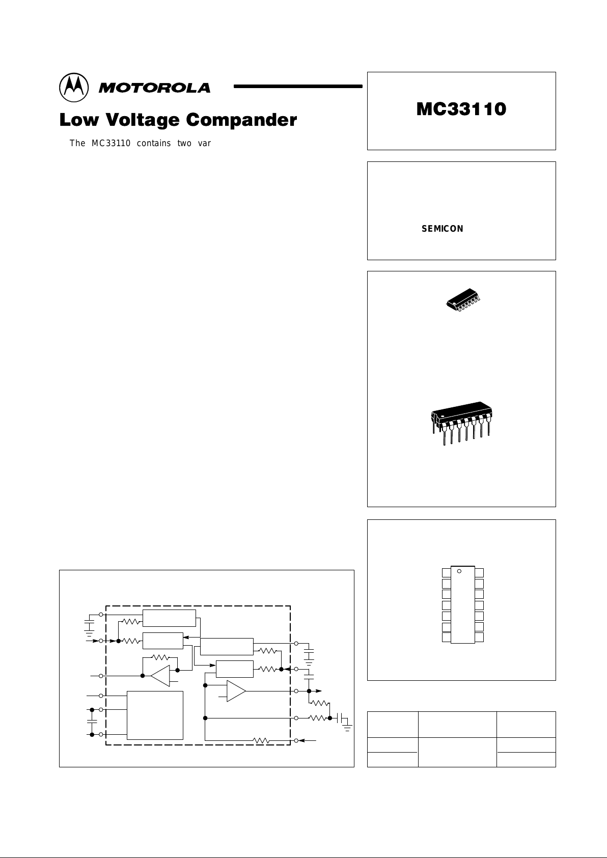
The MC33110 contains two variable gain circuits configured for
compressing and expanding the dynamic range of an audio signal. One
circuit is configured as an expander, while the other circuit can be configured
as a compressor or expander. Each circuit has a full wave rectifier to provide
average value information to a variable gain cell located in either the input
stage or the feedback path. An internal, temperature stable bandgap
reference provides the necessary precision voltages and currents required.
The MC33110 will operate from a supply voltage of 2.1 to 7.0 V, over a
temperature range of –40 to 85°C. The device is designed to accommodate
an 80 dB dynamic range from –60 dB to 20 dB, referenced to 100 mVrms.
Applications include cordless telephone, CB, walkie–talkie, most voice
RF links, and any application where the signal–to–noise ratio can be
improved by reducing the transmitted dynamic range. Other applications
include speakerphone and voice activated intercom, dictating machine,
standard telephone, etc.
The MC33110 is packaged in a 14 pin DIP for through–the–hole
applications and an SO–14 surface mount.
• Operating Supply Voltage: 2.1 to 7.0 V
• No Precision External Components Required
• 80 dB Dynamic Range Compressed to 40 dB, Re–expandable to 80 dB
• Unity Gain Level: 100 mVrms
• Adjustable Response Time
• Ambient Operating Temperature: –40 to 85°C
• Temperature Compensated Reference
• Applications Include Cordless Phone, CB Radio, Speakerphone, etc.
Simplified Block Diagram
+
–
+
–
2.2 µF
14
3
5
4
6
7
Gnd
10
µ
F
V
B
V
CC
Exp.
Output
Exp
Input
4.7 k
10 k
Rectifier
∆
Gain
10 k
V
B
Bias
&
Reference
Generator
V
B
∆
Gain
Rectifier
4.7 k
10 k
12
8
11
9
10
Comp
Input
1.0
µ
F
20 k
20 k
Comp
Output
2.0
µ
F
2.2
µ
F
10 k
Motorola, Inc. 1998 Rev 1
Page 2
MC33110
2
MOTOROLA RF/IF DEVICE DATA
PIN DESCRIPTION
Name Pin Description
V
ref
1 Normally this pin is not used and is left open. It can be used to make limited adjustments to
the 0 dB level. Any noise or leakage at this pin will affect the 0 dB level and gain tracking.
NC 2, 13 No connection. These pins are not internally connected.
Expander Filter 3 Connect to an external capacitor to filter the full wave rectifier’s output. This capacitor
affects attack and decay times, as well as low frequency accuracy.
Expander Output 4 Output of the expander amplifier.
Expander Input 5 The input impedance is nominally 3.2 kΩ. Nominal signal range is 3.16 mVrms to
316 mVrms. Must be capacitor coupled to the signal source.
V
B
6 An internal reference voltage, nominally VCC/2. This is an ac ground and must be well
filtered to obtain high power supply rejection and low crosstalk.
Ground 7 Connect to a clean power supply ground.
Compressor Feedback 8 Input to the compressor variable gain stage and rectifier. Normally the signal is supplied by
the compressor’s output (Pin 11). Input impedance is nominally 3.2 kΩ.
Inverting Input 9 Inverting input to the compressor amplifier. Normally, this is connected to the compressor’s
output through a filtered dc feedback path.
Compressor Input 10 The input impedance is nominally 10 kΩ. Nominal signal range is 100 µVrms to 1.0 Vrms.
Must be capacitor coupled to the signal source.
Compressor Output 11 Output of the compressor amplifier.
Compressor Filter 12 Connect to an external capacitor to filter the full wave rectifier’s output. This capacitor
affects attack & decay times, and low frequency accuracy.
V
CC
14 Power supply pin. Connect to a power supply providing between 2.1 V and 7.0 V . Nominal
current consumption is 3.5 mA.
1.0 V
100 mV
100
µ
V
1.0 mV
10 mV
316 mV
31.6 mV
10 mV
3.16 mV
+
–
+
–
Rectifier
∆
Gain
I
ref
V
B
R6
R5
V
out
R4
V
in
– 60 dB
– 50 dB
– 40 dB
– 30 dB
– 20 dB
– 10 dB
0 dB
10 dB
20 dB
V
in
R2
R1
∆
Gain
Rectifier
I
ref
R
S
V
B
V
out
Transfer FunctionsCompressor Expander
Compression Expansion
(Voltages are rms)
V
out
+
R5 x R6 x I
refxVin
7.2 x R4
Ǹ
+
0.3162 x V
in
Ǹ
V
out
+
7.2 x R3 x V
in
2
R1xR2xI
ref
+
10 x V
in
2
Page 3
MC33110
3
MOTOROLA RF/IF DEVICE DATA
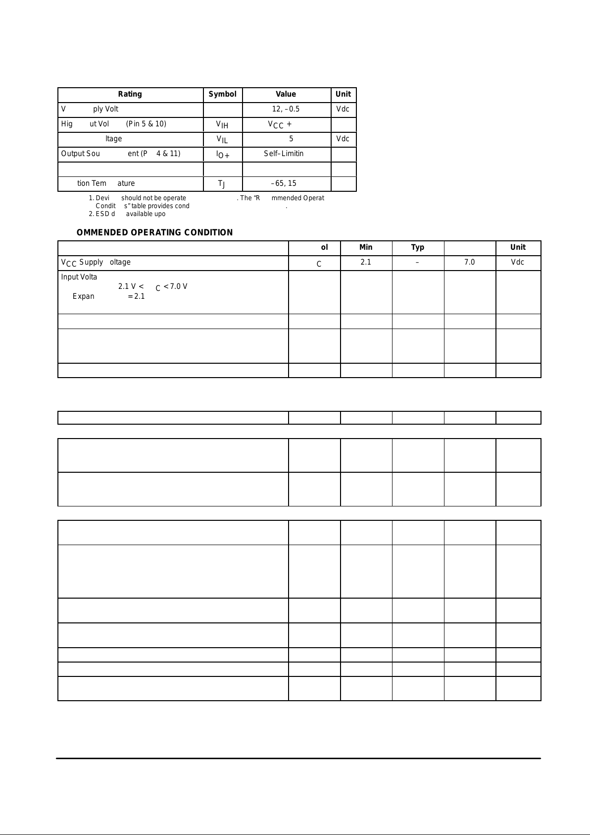
MAXIMUM RATINGS
Rating
Symbol
Value
Unit
VCC Supply Voltage
V
CC
12, –0.5
Vdc
High Input Voltage (Pin 5 & 10)
V
IH
VCC + 0.5
Vdc
Low Input Voltage
V
IL
–0.5
Vdc
Output Source Current (Pin 4 & 11)
I
O+
Self–Limiting
Output Sink Current
I
O–
20
mA
Junction Temperature
T
J
–65, 150
°C
NOTES: 1. Devices should not be operated at these values. The “Recommended Operating
Conditions” table provides conditions for actual device operation.
2.ESD data available upon request.
RECOMMENDED OPERATING CONDITIONS
Characteristic Symbol Min Typ Max Unit
VCC Supply Voltage V
CC
2.1 – 7.0 Vdc
Input Voltage Range
Compressor, 2.1 V < VCC < 7.0 V
Expander, VCC = 2.1 V
Expander, 3.0 V < VCC < 7.0 V
V
IR
0
0
0
–
–
–
1.0
0.25
0.316
Vrms
Input Frequency F
in
100 – 20 k Hz
Output Load
Compressor (Pin 11, VO = 100 mV)
Expander (Pin 4, VO = 100 mV)
R
L
300
150
–
–
∞
∞
Ω
Ambient Temperature T
A
–40 – 85 °C
All limits are not necessarily functional concurrently.
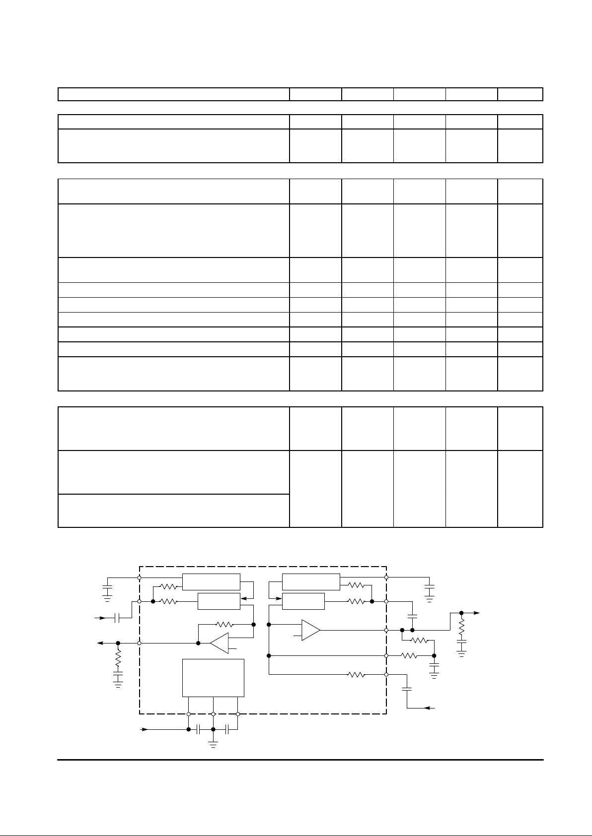
ELECTRICAL CHARACTERISTICS (V
CC
= 5.0 V , f = 1.0 kHz, unless otherwise noted, TA = 25°C, see Figure 1)
Characteristic
Symbol Min Typ Max Unit
POWER SUPPLY
Power Supply Current
VCC = 5.0 V
VCC = 2.1 V
I
CC
–
–
3.5
3.3
5.5
–
mA
VB Voltage
VCC = 5.0 V
2.1 V < VCC < 7.0 V
V
B
2.4
–
2.5
VCC/2
2.6
–
Vdc
COMPRESSOR
0 dB Gain
Vin = 100 mVrms, Pin 1 = Open
G
(CO)
–1.5 0 1.5
dB
Gain Tracking
@ Vin = 1.0 Vrms, output relative to G
(CO)
@ Vin = 10 mVrms, output relative to G
(CO)
@ Vin = 1.0 mVrms, output relative to G
(CO)
@ Vin = 100 µVrms, output relative to G
(CO)
G
t
9.0
–
–
–31
10
–10
–20
–30
11
–
–
–29
dB
Total Harmonic Distortion
Vin = 100 mVrms, f = 1.0 kHz
THD
0 0.1 1.5
%
Power Supply Rejection
f = 1.0 kHz, CVB = 10 µF, Vin = – 20 dB
PSRR
– 22 –
dB
Attack Time (Capacitor @ Pin 12 = 2.2 µF) t
a(C)
– 6.0 – ms
Decay Time (Capacitor @ Pin 12 = 2.2 µF) t
d(C)
– 20 – ms
Input Impedance Pin 10
Pin 8
R
in
–
–
10
3.2
–
–
kΩ
Page 4
MC33110
4
MOTOROLA RF/IF DEVICE DATA
ELECTRICAL CHARACTERISTICS
(VCC = 5.0 V , f = 1.0 kHz, unless otherwise noted, TA = 25°C, see Figure 1)
Characteristic UnitMaxTypMinSymbol
COMPRESSOR
Peak Output Current Pin 11 I
pk
– 0.3 – mA
Output Offset
Pin 11, with respect to Pin 6, NO SIGNAL
Change from NO SIGNAL to 1.0 Vrms at Input
V
OO
–150
–
0
50
150
–
mVdc
EXPANDER
0 dB Gain
(Vin = 100 mVrms, Pin 1 = open)
G
(EO)
–1.5 0 1.5
dB
Gain Tracking
@ Vin = 316 mVrms, output relative to G
(EO)
@ Vin = 31.6 mVrms, output relative to G
(EO)
@ Vin = 10 mVrms, output relative to G
(EO)
@ Vin = 3.16 mVrms, output relative to G
(EO)
G
t
19
–
–
–61
+ 20
– 20
– 40
– 60
21
–
–
–59
dB
Total Harmonic Distortion
Vin = 100 mVrms, f = 1.0 kHz
THD
0 0.06 1.5
%
Power Supply Rejection (f = 1.0 kHz, CVB = 10 µF) PSRR – 37 – dB
Attack Time (Capacitor @ Pin 3 = 2.2 µF) t
a(E)
– 19 – ms
Decay Time (Capacitor @ Pin 3 = 2.2 µF) t
d(E)
– 20 – ms
Input Impedance Pin 5 R
in
– 3.2 – kΩ
Peak Output Current Pin 4 I
pk
– 1.0 – mA
Output Offset
Pin 4, with respect to Pin 6, NO SIGNAL
Change from NO SIGNAL to 316 mVrms at Input
V
OO
–150
–
0
25
150
–
mVdc
MISCELLANEOUS
Gain (Pin 10 to Pin 4; Pin 11 capacitor coupled to Pin 5)
VCC = 7.0 V , Vin = 1.0 Vrms
VCC = 3.0 V , Vin = 1.0 Vrms
VCC = 2.1 V , Vin = 31.6 mVrms
A
V
–2.5
–2.5
–2.5
0
0
0
2.5
2.5
2.5
dB
Channel Separation
Expander to Compressor, output measured at Pin 11
Vin @ Pin 5 = 316 mVrms, f = 1.0 kHz
Vin @ Pin 5 = 316 mVrms, f = 10 kHz
CS
43
–
48
68
–
–
dB
Compressor to Expander, output measured at Pin 4
Vin @ Pin 10 = 1.0 Vrms, f = 1.0 kHz
Vin @ Pin 10 = 1.0 Vrms, f = 10 kHz
65
–
107
114
–
–
Figure 1. Test Circuit
+
–
+
–
2.2 µF
2 µF
5.0 k
3.0
µ
F
Expander
Input
Expander
Output
V
CC
4.7
µ
F 4.7 µF
14 7 6
3
5
4
4.7 k
10 k
Rectifier
∆
Gain
Rectifier
∆
Gain
V
B
V
B
10 k
V
B
Bias &
Reference
Generator
4.7 k
10 k
10 k
12
8
11
9
10
2.0
µ
F
1.0 µF
3.0
µ
F
5.0 k
2.2
µ
F
Compressor
Output
1.0
µ
F
Compressor
Input
10 k
10 k
Page 5

MC33110
5
MOTOROLA RF/IF DEVICE DATA
Figure 2. Compressor Transfer Characteristics
20
0
–20
–60
+100–20–30
Vin, INPUT VOLTAGE (dB)
V
out
, OUTPUT VOL TAGE (dB)
–10
–40
Compressor Expander
Figure 3. Expander Transfer Characteristics
1000
100
10
1.0
1000100101.00.1
Vin, INPUT VOLTAGE (mVrms)
V
out
, OUTPUT VOL TAGE (mVrms)
Figure 4. Compressor Transfer Characteristics
1000
100
10
0.1
1000100101.0
Vin, INPUT VOLTAGE (mVrms)
V
out
, OUTPUT VOL TAGE (mVrms)
Figure 5. Expander Transfer Characteristics
10
0
–10
–30
+200–40–60
Vin, INPUT VOLTAGE (dB)
V
out
, OUTPUT VOL TAGE (dB)
–20
–20
Figure 6. Power Supply Rejection (Compressor)
40
30
20
–10
100 k10 k10010
f, FREQUENCY (Hz)
REJECTION (dB)
1.0 k
10
0
Figure 7. Power Supply Rejection (Expander)
50
30
20
100 k10 k10010
f, FREQUENCY (Hz)
REJECTION (dB)
1.0 k
10
0
40
1.0
0 dB = 100 mVrms0 dB = 100 mVrms
CVB = 220 µF
CVB = 100 µF
CVB = 47 µF
CVB = 10 µF
Pin 10 Input Signal = 0 mV
VCC = 5.0 V
CVB = 220 µF
CVB = 100 µF
CVB = 47 µF
CVB = 10 µF
Pin 5 Input Signal = 0 mV
VCC = 5.0 V
Page 6

MC33110
6
MOTOROLA RF/IF DEVICE DATA
Compressor Expander
Figure 8. Power Supply Rejection (Compressor)
40
30
20
–10
100 k10 k10010
f, FREQUENCY (Hz)
REJECTION (dB)
1.0 k
10
0
Figure 9. Power Supply Rejection (Expander)
50
30
20
100 k10 k10010
f, FREQUENCY (Hz)
REJECTION (dB)
1.0 k
10
0
40
CVB = 220 µF
CVB = 100 µF
CVB = 47 µF
CVB = 10 µF
Pin 10 Input Signal = –20 dB
VCC = 5.0 V
CVB = 220 µF
CVB = 100 µF
CVB = 47 µF
CVB = 10 µF
Figure 10. Frequency Response (Compressor)
1.0
–3.0
–5.0
100 k10 k100
f, FREQUENCY (Hz)
OUTPUT RELA TIVE T O INPUT (dB)
1.0 k
–7.0
–11
–1.0
Pin 5 Input Signal = –10 dB
VCC = 5.0 V
–9.0
20 k
Figure 11. Frequency Response (Expander)
11
7.0
5.0
100 k10 k100
f, FREQUENCY (Hz)
OUTPUT RELA TIVE T O INPUT (dB)
1.0 k
3.0
–1.0
9.0
1.0
20 k
Figure 12. Frequency Response (Compressor)
60
40
30
100 k10 k100
f, FREQUENCY (Hz)
OUTPUT RELA TIVE T O INPUT (dB)
1.0 k
20
0
50
10
20 k
Figure 13. Frequency Response (Expander)
0
–20
–30
100 k10 k100
f, FREQUENCY (Hz)
OUTPUT RELA TIVE T O INPUT (dB)
1.0 k
–40
–60
–10
–50
20 k
Vin = 100 mVrms
Vin = 1.0 Vrms
Vin = 316 mVrms
Vin = 100 mVrms
Vin = 100 µVrms
Vin = 1.0 mVrms
Vin = 10 mVrms
Vin = 3.16 mVrms
Page 7

MC33110
7
MOTOROLA RF/IF DEVICE DATA
Attack Time
Figure 14. Attack and Decay Times (Compressor)
100
60
40
104.00
C, CAPACITANCE AT PIN 12 (µF)
MILLISECONDS (ms)
2.0
20
0
80
6.0 8.0
Figure 15. Attack and Decay Times (Expander)
100
60
40
104.00
C, CAPACITANCE AT PIN 3 (µF)
MILLISECONDS (ms)
2.0
20
0
80
6.0 8.0
Output
(Pin 11)
Input
(Pin 10)
∆
V1
∆
V2
Attack Time = Time to 63% of ∆V1.
Decay Time = Time to 63% of ∆V2.
Figure 16. Attack and Decay Times (Compressor)
Attack Time = Time to 63% of ∆V1.
Decay Time = Time to 63% of ∆V2.
Figure 17. Attack and Decay Times (Expander)
Output
(Pin 4)
Input
(Pin 5)
∆
V1
∆
V2
Figure 18. Maximum Input Signal
3.0
2.0
7.04.0
VCC, SUPPLY VOLTAGE (V)
2.0
1.0
0
5.0 6.03.0
V
in
, INPUT VOLTAGE (Vrms)
Figure 19. Channel Separation
120
100
100 k10 k
f, FREQUENCY (Hz)
100
60
40
20 k1.0 k
SEPARATION (dB)
80
Decay Time
Compressor
Expander
Compressor To Expander
Expander To Compressor
Page 8

MC33110
8
MOTOROLA RF/IF DEVICE DATA
Compressor Expander
Figure 20. Compressor Gain Tracking
versus Temperature
1.0
–1.0
8520–20–40
TA, AMBIENT TEMPERATURE (
°
C)
0
0
Figure 21. Expander Gain Tracking
versus Temperature
1.0
8520–20–40
TA, AMBIENT TEMPERATURE (
°
C)
0
0
–1.0
Figure 22. Compressor THD versus Temperature
TA, AMBIENT TEMPERATURE (°C)
Figure 23. Expander THD versus Temperature
TA, AMBIENT TEMPERATURE (°C)
40 60
Shaded Area Depicts Typical Drift Range
100
µ
Vrms ≤ Vin ≤ 1 Vrms
6040
10
–10
0
8520–20–40 0 8520–20–40 040 60 6040
20
–20
0
GAIN DRIFT versus +25 C (dB)
°
THD DRIFT versus +25 C (%%)
°
GAIN DRIFT versus +25 C (dB)
°
Shaded Area Depicts Typical Drift Range
3.16 mVrms
≤
Vin ≤ 316 mVrms
THD DRIFT versus +25 C (%%)
°
FUNCTIONAL DESCRIPTION
Introduction
The MC33110 compander (COMpressor and exPANDER)
is composed of two variable gain circuits which provide
compression and expansion of the signal dynamic range.
The compressor will take a signal with an 80 dB dynamic
range (100 µV to 1.0 Vrms), and reduce that to a 40 dB
dynamic range by attenuating strong signals, while
amplifying low level signals. The expander does the opposite
in that the 40 dB signal range is increased to a dynamic
range of 80 dB by amplifying strong signals and attenuating
low level signals. The 0 dB level is internally set at 100
mVrms — that is the signal level which is neither amplified
nor attenuated. Both circuits contain the necessary precision
full wave rectifier, variable gain cell, and temperature
compensated references required for accurate and stable
performance.
Note: All dB values mentioned in this data sheet, unless
otherwise noted, are referred to 100 mVrms.
Page 9

MC33110
9
MOTOROLA RF/IF DEVICE DATA
Figure 24. Compressor
+
–
2.2 µF
12
10
Input
10 k
I
ref
V
CC
Rectifier
I
Control
10 k
∆
Gain
V
B
8
11
9
20 k
R2
20 k
R1
1.0 µF
C1
Output
2.0
µ
F
4.7 k
Compressor
The compressor is an operational amplifier with a fixed
input resistor and a variable gain cell in its feedback path as
shown in Figure 24.
The amplifier output is sampled by the precision rectifier
which, in turn, supplies a DC signal (I
Control
), representative
of the rectifier’s AC signal, to the variable gain cell. The
reference current (I
ref
) is an internally generated precision
current. The effective impedance of the variable gain cell
varies with the ratio of the two currents, and decreases as
I
Control
increases, thereby providing compression. The output
is related to the input by the following equation:
V
out
= 0.3162 x √V
in
(Equation 1)
In terms of dB levels, the relationship is:
V
out(dB)
= 0.5 x V
in(dB)
(Equation 2)
where 0 dB = 100 mVrms (see Figure 2 and 4).
The inputs and output are internally biased at VB (V
CC/2
),
and must therefore be capacitor coupled to external circuitry.
Pin 10 input impedance is nominally 10 kΩ (± 20%), and the
maximum functional input signal is shown in Figure 18. Bias
currents required by the op amp and the variable gain cell are
internally supplied. Due to clamp diodes at the input (to V
CC
and ground), the input signal must be maintained between
the supply rails. If the input signal goes more than 0.5 V
above VCC or below ground, excessive currents will flow and
distortion will show up at the output.
When no AC signals are present at the input, the variable
gain cell will attempt to set such a high gain that the circuit
may be come unstable. For this reason resistors R1 and R2,
and capacitor C1 are added to provide DC stability. The pole
formed by R1, R2 and C1 should have a pole frequency no
more than 1/10th of the lowest frequency of interest. The pole
frequency is calculated from:
f
+
R1)R2
2pxR1R2C3
(Equation 3)
for the component values shown, the pole frequency is
≈ 16 Hz.
Likewise, the capacitor between Pins 11 and 8 should be
selected such that, in conjunction with the input impedance at
Pin 8 (≈ 3200 Ω, ± 20%), the resulting pole frequency is no
more than 1/10 of the lowest frequency of interest. With the
components shown, the pole frequency is < 30 Hz. This pole
frequency is calculated from:
f
+
1
2px3.2kxC
(Equation 4)
The output of the rectifier is filtered by the capacitor at
Pin 12, which, in conjunction with an internal 10 k resistor,
provides the time constant for the attack and decay times.
Figure 14 and 16 indicate how the times vary with the
capacitor value. The attack time for the compressor is always
faster than the decay time due to the fact that the rectifier is
fed from the output rather than the input. Since the output is
initially larger than expected (immediately after the input has
increased), the external capacitor is charged more quickly
during the initial part of the time constant. When the input is
decreased, the time constant is closer to that calculated by
t = RC. If the attack and decay times are decreased by using
a smaller capacitor, performance at low frequencies will
degrade.
Page 10

MC33110
10
MOTOROLA RF/IF DEVICE DATA
Figure 25. Expander
2.2 µF
I
ref
Rectifier
I
Control
10 k
∆
Gain
V
B
Output
4.7 k
+
–
Input
5
V
CC
10 k
3
4
Expander
The expander is an operational amplifier with a fixed
feedback resistor and a variable gain cell in its input path as
shown in Figure 25.
The input signal is sampled by the precision rectifier
which, in turn, supplies a dc signal (I
Control
), representative
of the ac input signal, to the variable gain cell. The reference
current (I
ref
) is an internally generated precision current. The
effective impedance of the variable gain cell varies with the
ratio of the two currents, and decreases as I
Control
increases,
thereby providing expansion. The output is related to the
input by the following equation:
V
out
= 10 x (Vin)
2
(Equation 5)
In terms of dB levels, the relationship is:
V
out(dB)
= 2.0 x V
in(dB)
(Equation 6)
where 0 dB = 100 mVrms (see Figure 3 and 5).
The inputs and output are internally biased at VB(V
CC/2
),
and must therefore be capacitor coupled to external circuitry.
The input impedance at Pin 5 is nominally 3.2 kΩ (±20%),
and the maximum functional input signal is shown in
Figure 18. Bias currents required by the op amp and the
variable gain cell are internally supplied. Due to clamp diodes
at the input (to VCC and ground), the input signal must be
maintained between the supply rails. If the input signal goes
more than 0.5 V above VCC or below ground, excessive
currents will flow, and distortion will show up at the output.
The output of the rectifier is filtered by the capacitor at
Pin 3, which, in conjunction with an internal 10 k resistor,
provides the time constant for the attack and decay times.
Figure 15 and 17 indicate how the times vary with the
capacitor value. If the attack and decay times are decreased
by using a smaller capacitor, performance at low frequencies
will degrade.
Power Supply
The MC33110 requires a power supply voltage between
2.1 V and 7.0 V , and a nominal current of 3.5 mA. The supply
voltage should be well filtered and free of ripple. A minimum
of 4.7 µF in parallel with a 0.01 µF capacitor is recommended
for filtering and RF bypass.
VB (Pin 6) is an internally generated mid supply reference,
and is used internally as an ac ground. The external capacitor
at Pin 6 filters this voltage, and its value affects the power
supply noise rejection as shown in Figures 6 through 9. This
reference voltage may be used to bias external circuitry as
long as the current draw is limited to <10 µA.
Page 11

MC33110
11
MOTOROLA RF/IF DEVICE DATA
APPLICATIONS INFORMATION
Signal–to–Noise Improvement
Among the basic reasons for the original development of
compander type circuits was to improve the signal–to–noise
ratio of long distance telecom circuits, and of voice circuits
which are transmitted over RF links (CBs, walkie–talkies,
cordless phones, etc.). Since much of the noise heard at the
receiving end of a transmission is due to noise picked up, for
example, in the airway portion of the RF link, the compressor
was developed to increase the low–level signals at the
transmitting end. Then any noise picked in the RF link would
be a smaller percentage of the transmitted signal level. At the
receiving end, the signal is then expanded back to its original
level, retaining the same high signal–to–noise ratio. While the
above explanation indicates it is not necessary to attenuate
strong signals (at the transmitting end), a benefit of doing this
is the reduced dynamic range which must be handled by the
system transmitter and receiver. The MC33110 was
designed for a two–to–one compression and expansion, i.e.
an 80 dB dynamic signal is compressed to a 40 dB dynamic
range, transmitted to the receiving end and then expanded
back to an 80 dB dynamic range.
The MC33110 compander is not limited to RF or long
distance telephony applications. It can be used in any system
requiring an improved signal–to–noise ratio such as
telephones, speakerphones, tape recorders, digital
recording, and many others.
Second Expander
Should the application require it, the MC33110 can be
configured as two expanders by reconfiguring the
compressor side as shown in Figure 26.
Figure 26. Second Expander
2.2 µF
I
ref
Rectifier
I
Control
10 k
∆
Gain
V
B
Output
4.7 k
+
–
Input
8
10 k
12
11
9
10
This circuit will provide the same performance as
the expander at Pins 3 through 5.
Power Supplies, Grounding
The PC board layout, the quality of the power supplies and
the ground system at the IC are very important in order to
obtain proper operation. Noise, from any source, coming into
the device on VCC or ground, can cause a distorted output, or
incorrect gain level.
VCC must be decoupled to the appropriate ground at the
IC (within 1″ max) with a 4.7 µF capacitor and a 0.01 µF
ceramic. A tantalum capacitor is recommended for the larger
value if very high frequency noise is present since electrolytic
capacitors simply have too much inductance at those
frequencies. The quality of the power supply voltage should
be checked at the IC with a high frequency scope. Noise
spikes (always present if digital circuits are near this IC) can
easily exceed 400 mV, and if they get into the IC, the output
can have noise or distortion. Noise can be reduced by
inserting resistors and/or inductors between the supply and
the IC.
If switching power supplies are used, there will usually be
spikes of 0.5 V or greater at frequencies of 50 kHz to
1.0 MHz. These spikes are generally more difficult to reduce
because of their greater energy content. In extreme cases, a
three terminal regulator (MC78L05ACP), with appropriate
high frequency filtering, should be used and dedicated to the
analog portion of the circuit.
The ripple content of the supply should not allow its
magnitude to exceed the values in the Recommended
Operating Conditions table.
The PC board tracks supplying VCC and ground to the
MC33110 should preferably not be at the tail end of the bus
distribution, after passing through a maze of digital circuitry.
The analog circuitry containing the MC33110 should be close
to the power supply, or the connector where the supply
voltages enter the board. If VCC is supplying considerable
current to other parts of the board, then it is preferable to
have dedicated lines from the supply or connector directly to
the MC33110 and associated circuitry.
PC Board Layout
Although this device is intended for use in the audio
frequency range, the amplifiers have a bandwidth of
≈300 kHz, and can therefore oscillate at frequencies outside
the voiceband should there be excessive stray capacitance
or other unintended feedback loops. A solid ground plane is
Page 12

MC33110
12
MOTOROLA RF/IF DEVICE DATA
strongly recommended to minimize coupling of any digital
noise into the analog section. Use of wire wrapped boards
should definitely be avoided.
Since many applications of the MC33110 compander
involve voice transmission over RF links, care must be taken
in the design of the product to keep RF signals out of the
MC33110 and associated circuitry. This involves proper
layout of the PC boards, the physical arrangement of the
boards, shielding, proper RF ground, etc.
GLOSSARY
Attack Time — The settling time for a circuit after its input
signal has been increased.
Attenuation — A decrease in magnitude of a
communication signal, usually expressed in dB.
Bandwidth — The range of information carrying frequencies
of a communication system.
Channel Separation — The ability of one circuit to reject
outputting signals which are being processed by another
circuit. Also referred to as crosstalk, it is usually expressed in
dB.
Compander — A contraction of the words compressor and
expander. A compander is composed of two circuits, one of
each kind.
Compressor — A circuit which compresses or reduces the
dynamic range of a signal by attenuating strong signals and
amplifying low level signals.
dB — A power or voltage measurement unit, referred to
another power or voltage. It is generally computed as:
10 x log (P1/P2) for power measurements, and
20 x log (V1/V2) for voltage measurements.
dBm — An indication of signal power. 1.0 mW across 600 Ω
or 0.775 V rms, is typically defined as 0 dBm for telecom
applications. Any voltage level is converted to dBm by:
dBm = 20 x log (Vrms/0.775), or
dBm = [20 x log (Vrms)] + 2.22.
dBrn — Indicates a dBm measurement relative to 1.0 pW
power level into 600 Ω. Generally used for noise
measurements, 0 dBrn = – 90 dBm.
dBrnC — Indicates a dBrn measurement using a
C–message weighting filter.
Decay Time — The settling time for a circuit after its input
signal has been decreased.
Expander — A circuit which expands or increases the
dynamic range of a signal by amplifying strong signals and
attenuating low level signals.
Gain — The change in signal amplitude (increase or
decrease) after passing through an amplifier, or other circuit
stage. Usually expressed in dB, an increase is a positive
number and a decrease is a negative number.
Power Supply Rejection Ratio — The ability of a circuit to
reject outputting noise, or ripple, which is present on the
power supply lines. PSRR is usually expressed in dB.
Signal–to–Noise Ratio — The ratio of the desired signal to
unwanted signals (noise) within a defined frequency range.
The larger the number, the better.
Voiceband — That portion of the audio frequency range
used for transmission across the telephone system.
Typically, it is 300 to 3400 Hz.
Page 13

MC33110
13
MOTOROLA RF/IF DEVICE DATA
D SUFFIX
PLASTIC PACKAGE
CASE 751A-03
(SO–14)
ISSUE F
P SUFFIX
PLASTIC PACKAGE
CASE 646–06
ISSUE M
OUTLINE DIMENSIONS
NOTES:
1. LEADS WITHIN 0.13 (0.005) RADIUS OF TRUE
POSITION AT SEATING PLANE AT MAXIMUM
MATERIAL CONDITION.
2. DIMENSION L TO CENTER OF LEADS WHEN
FORMED PARALLEL.
3. DIMENSION B DOES NOT INCLUDE MOLD
FLASH.
4. ROUNDED CORNERS OPTIONAL.
17
14 8
B
A
F
HG D
K
C
N
L
J
M
SEATING
PLANE
DIM MIN MAX MIN MAX
MILLIMETERSINCHES
A 0.715 0.770 18.16 19.56
B 0.240 0.260 6.10 6.60
C 0.145 0.185 3.69 4.69
D 0.015 0.021 0.38 0.53
F 0.040 0.070 1.02 1.78
G 0.100 BSC 2.54 BSC
H 0.052 0.095 1.32 2.41
J 0.008 0.015 0.20 0.38
K 0.115 0.135 2.92 3.43
L 0.300 BSC 7.62 BSC
M 0 10 0 10
N 0.015 0.039 0.39 1.01
____
NOTES:
1. DIMENSIONING AND TOLERANCING PER ANSI
Y14.5M, 1982.
2. CONTROLLING DIMENSION: MILLIMETER.
3. DIMENSIONS A AND B DO NOT INCLUDE
MOLD PROTRUSION.
4. MAXIMUM MOLD PROTRUSION 0.15 (0.006)
PER SIDE.
5. DIMENSION D DOES NOT INCLUDE DAMBAR
PROTRUSION. ALLOWABLE DAMBAR
PROTRUSION SHALL BE 0.127 (0.005) TOTAL
IN EXCESS OF THE D DIMENSION AT
MAXIMUM MATERIAL CONDITION.
–A–
–B–
G
P 7 PL
14 8
71
M
0.25 (0.010) B
M
S
B
M
0.25 (0.010) A
S
T
–T–
F
R
X 45
SEATING
PLANE
D 14 PL
K
C
J
M
_
DIM MIN MAX MIN MAX
INCHESMILLIMETERS
A 8.55 8.75 0.337 0.344
B 3.80 4.00 0.150 0.157
C 1.35 1.75 0.054 0.068
D 0.35 0.49 0.014 0.019
F 0.40 1.25 0.016 0.049
G 1.27 BSC 0.050 BSC
J 0.19 0.25 0.008 0.009
K 0.10 0.25 0.004 0.009
M 0 7 0 7
P 5.80 6.20 0.228 0.244
R 0.25 0.50 0.010 0.019
____
Motorola reserves the right to make changes without further notice to any products herein. Motorola makes no warranty , representation or guarantee regarding
the suitability of its products for any particular purpose, nor does Motorola assume any liability arising out of the application or use of any product or circuit, and
specifically disclaims any and all liability, including without limitation consequential or incidental damages. “T ypical” parameters which may be provided in Motorola
data sheets and/or specifications can and do vary in different applications and actual performance may vary over time. All operating parameters, including “Typicals”
must be validated for each customer application by customer’s technical experts. Motorola does not convey any license under its patent rights nor the rights of
others. Motorola products are not designed, intended, or authorized for use as components in systems intended for surgical implant into the body, or other
applications intended to support or sustain life, or for any other application in which the failure of the Motorola product could create a situation where personal injury
or death may occur. Should Buyer purchase or use Motorola products for any such unintended or unauthorized application, Buyer shall indemnify and hold Motorola
and its officers, employees, subsidiaries, affiliates, and distributors harmless against all claims, costs, damages, and expenses, and reasonable attorney fees
arising out of, directly or indirectly, any claim of personal injury or death associated with such unintended or unauthorized use, even if such claim alleges that
Motorola was negligent regarding the design or manufacture of the part. Motorola and are registered trademarks of Motorola, Inc. Motorola, Inc. is an Equal
Opportunity/Affirmative Action Employer.
Mfax is a trademark of Motorola, Inc.
How to reach us:
USA/EUROPE /Locations Not Listed: Motorola Literature Distribution; JAPAN: Nippon Motorola Ltd.; SPD, Strategic Planning Office, 141,
P.O. Box 5405, Denver, Colorado 80217. 1–303–675–2140 or 1–800–441–2447 4–32–1 Nishi–Gotanda, Shinagawa–ku, Tokyo, Japan. 81–3–5487–8488
Customer Focus Center: 1–800–521–6274
Mfax: RMFAX0@email.sps.mot.com – TOUCHTONE 1–602–244–6609 ASIA/P ACIFIC: Motorola Semiconductors H.K. Ltd.; 8B Tai Ping Industrial Park,
Moto rola Fax Back Sys tem – US & Canada ONLY 1–800–774–1848 51 Ting Kok Road, Tai Po, N.T., Hong Kong. 852–26629298
– http://sps.motorola.com/mfax/
HOME PAGE: http://motorola.com/sps/
MC33110/D
◊
 Loading...