

Page 1
QUAD D-TYPEREGISTER (3-STATE)
.HIGH SPEED
f
= 73 MHz(TYP.) at VCC=5V
MAX
.LOWPOWERDISSIPATION
ICC=4µA(MAX.) at TA=25°C
.HIGH NOISEIMMUNITY
V
NIH=VNIL
=28%VCC(MIN.)
.OUTPUT DRIVE CAPABILITY
15 LSTTL LOADS
.SYMMETRICALOUTPUT IMPEDANCE
|IOH|=IOL=6 mA(MIN.)
.BALANCEDPROPAGATION DELAYS
t
PLH=tPHL
.WIDE OPERATINGVOLTAGE RANGE
VCC(OPR)= 2V to 6V
.PIN AND FUNCTION COMPATIBLE WITH
54/74LS 173
M54HC173
M74HC173
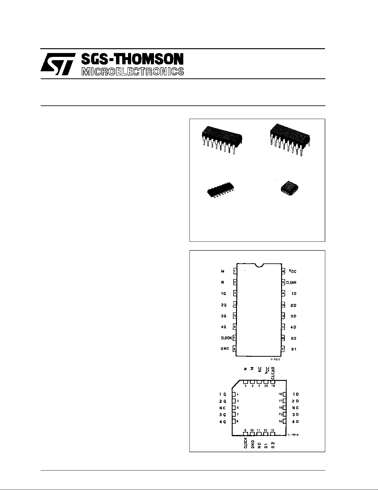
B1R
(PlasticPackage)
M1R
(MicroPackage)
ORDER CODES :
M54HC 173F1R M74H C173M1R
M74HC 173B1R M74HC1 73C1R
F1R
(CeramicPackage)
C1R
(Chip Carrier)
DESCRIPTION
TheM54/74HC173is ahighspeedCMOSQUADDTYPE REGISTER (3-STATE) fabricated in silicon
gate C2MOStechnology.
It has the same high speed performance of LSTTL
combined withtrue CMOSlowpower consumption.
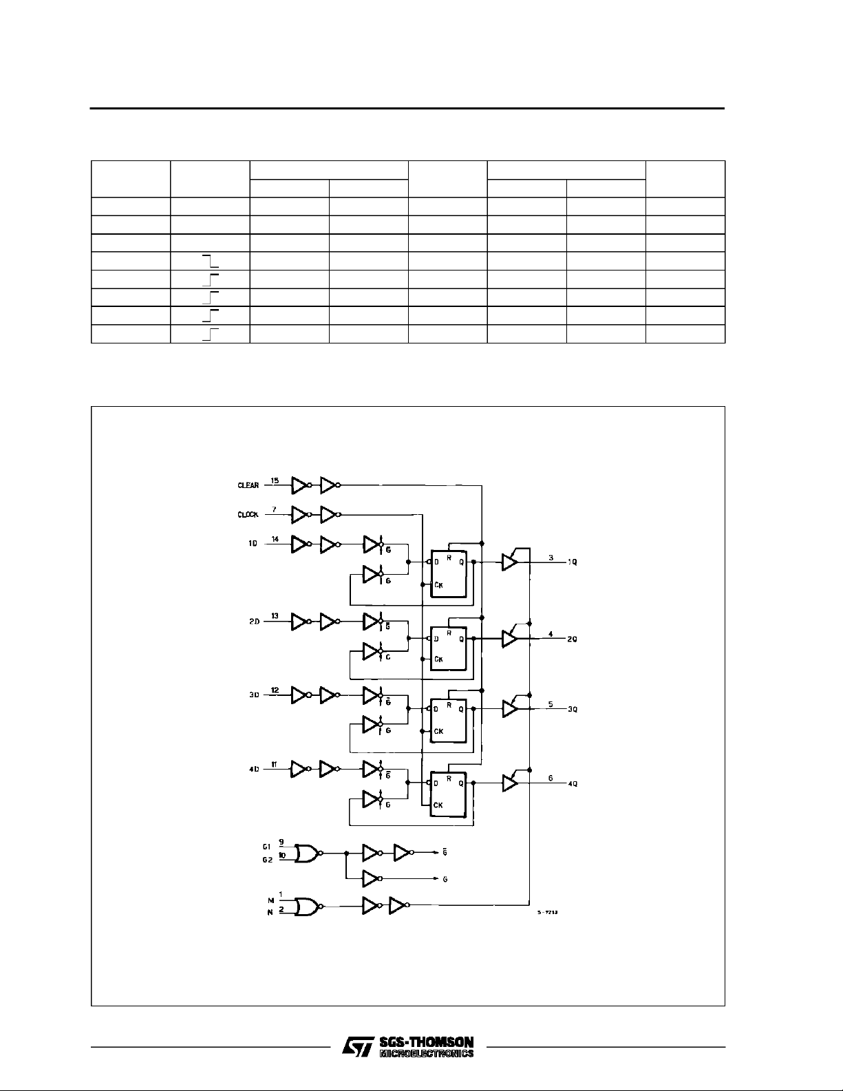
Thisdeviceiscomposedofa four-bit register includingD-typeflip-flopsand3-state buffers. Thefourflipflops are controlled by a common clock input
(CLOCK)and acommonresetinput (CLEAR). Signals applied to the datainputs (D1-D4) arestored at
the respective flip-flops on the positive going transition of theclock input, onlywhen both clock control
inputs (G1and G2) are held low.
The reset feature is asynchronous andactive high.
The stored data are provided on each outputonly
when bothoutput control inputs(M and N) are held
low,otherwise theoutputsgotothehigh-impedance
state.
All inputs are equipped with protection circuits
against static discharge and transient excess voltage.
PIN CONNECTIONS(top view)
NC =
No Internal
Connection
October 1992
1/12
Page 2
M54/M74HC173
TRUTH TABLE
CLEAR CLOCK
XXXXXHXZ
XXXXXXHZ
HXXXXLLL
LXXXLLQ0
LHXXLLQ0
LXHXLLQ0
LLLHLLH
L LLLLLL
X:Don’tCare Z:HighImpedance
DATA ENABLE
G1 G2 M N
Dn
OUTPUT CONTROL
Qn
LOGI C DI AG RAM
2/12
Page 3
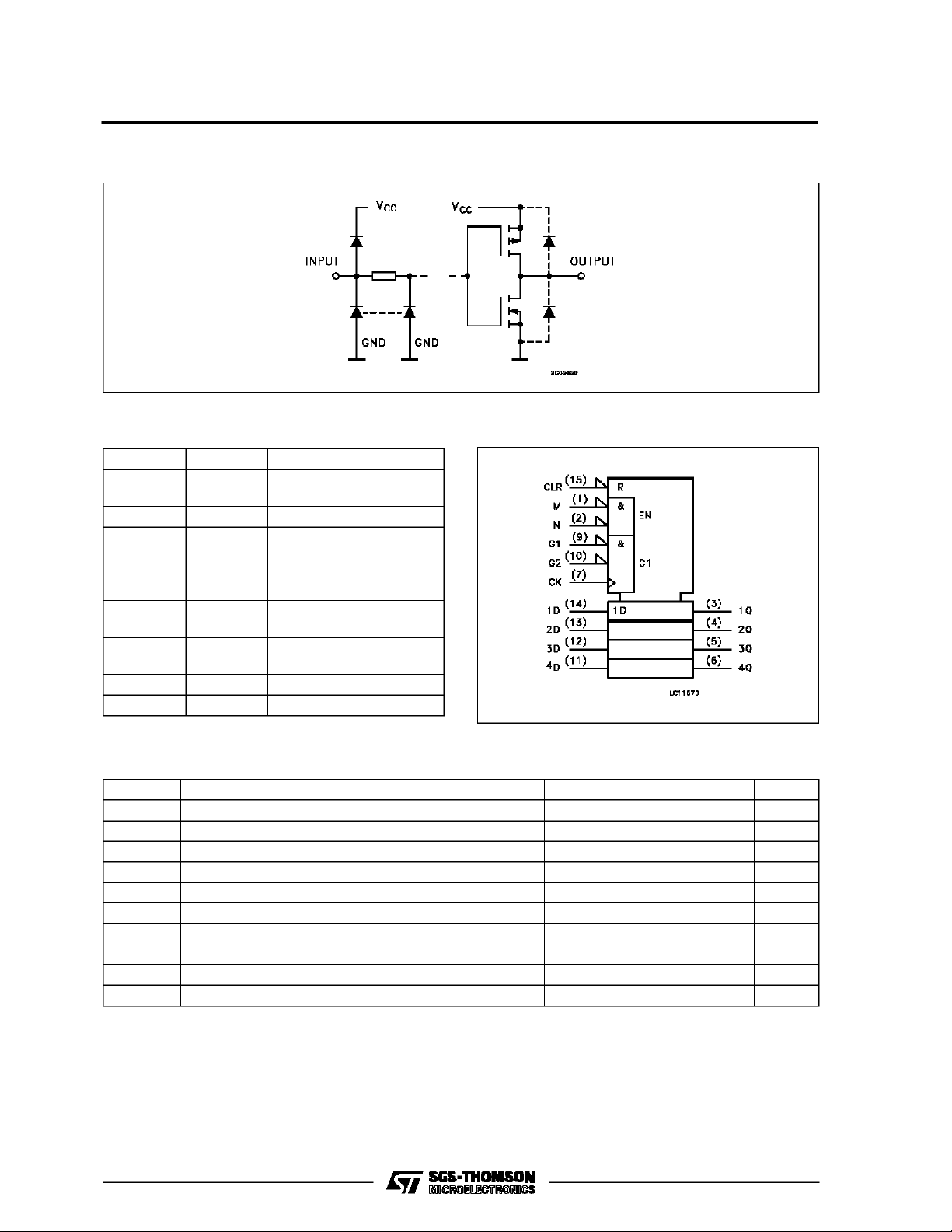
INPUT AND OUTPUT EQUIVALENT CIRCUIT
M54/M74HC173
PIN DESC RIPTION
IEC LOGIC SYMBOL
PIN No SYMBOL NAME AND FUNCTION
1, 2 M, N Output Enable Input
(Active LOW)
3, 4, 5, 6 1Q to 4Q 3-State Flip-flop Outputs
7 CLOCK Clock Input (LOW to
HIGH, Edge-triggered)
9, 10 G1, G2 Data Enable Inputs
(Active LOW)
14, 13, 12,111D to 4D Data Inputs
15 CLEAR Asynchronous Master
Reset (Active HIGH)
8 GND Ground (0V)
16 V
CC
Positive Supply Voltage
ABSOLU TE M AXIMU M R AT ING
Symbol Parameter Value Unit
V
CC
V
V
O
I
IK
I
OK
I
O
I
or I
CC
P
D
T
stg
T
AbsoluteMaximumRatingsarethose values beyond whichdamage tothedevicemayoccur. Functional operation under these conditionisnotimplied.
(*)500 mW: ≅ 65oC derateto300mWby 10mW/oC: 65oCto85oC
Supply Voltage -0.5 to +7 V
DC Input Voltage -0.5 to VCC+ 0.5 V
I
DC Output Voltage -0.5 to VCC+ 0.5 V
DC Input Diode Current ± 20 mA
DC Output Diode Current ± 20 mA
DC Output Source Sink Current Per Output Pin ± 35 mA
DC VCCor Ground Current ± 70 mA
GND
Power Dissipation 500 (*) mW
Storage Temperature -65 to +150
Lead Temperature (10sec) 300
L
o
C
o
C
3/12
Page 4
M54/M74HC173
RECO MM ENDED OPERATING CO NDI TIONS
Symbol Parameter Value Unit
V
V
V
T
t
r,tf
DC SPECIFICATIONS
Symbol Parameter
V
IH
V
V
OH
V
OL
I
I
OZ
I
CC
Supply Voltage 2 to 6 V
CC
Input Voltage 0 to V
I
Output Voltage 0 to V
O
Operating Temperature: M54HC Series
op
M74HC Series
CC
CC
-55 to +125
-40 to +85
Input Rise and Fall Time VCC= 2 V 0 to 1000 ns
V
= 4.5 V 0 to 500
CC
V
= 6 V 0 to 400
CC
Test Conditions Value
V
(V)
CC
=25oC
T
A
54HC and 74HC
-40 to 85oC
74HC
-55 to 125oC
Min. Typ. Max. Min. Max. Min. Max.
High Level Input
Voltage
2.0 1.5 1.5 1.5
4.5 3.15 3.15 3.15
6.0 4.2 4.2 4.2
Low Level Input
IL
Voltage
2.0 0.5 0.5 0.5
4.5 1.35 1.35 1.35
6.0 1.8 1.8 1.8
High Level
Output Voltage
Low Level Output
Voltage
Input Leakage
I
Current
3 State Output
Off State Current
Quiescent Supply
2.0
V
=
I
4.5 4.4 4.5 4.4 4.4
6.0 5.9 6.0 5.9 5.9
4.5 I
6.0 I
2.0
4.5 0.0 0.1 0.1 0.1
6.0 0.0 0.1 0.1 0.1
4.5 I
6.0 I
6.0
IO=-20 µA
V
IH
or
V
IL
=-6.0 mA 4.18 4.31 4.13 4.10
O
=-7.8 mA 5.68 5.8 5.63 5.60
O
V
=
I
IO=20µA
V
IH
or
V
IL
= 6.0 mA 0.17 0.26 0.37 0.40
O
= 7.8 mA 0.18 0.26 0.37 0.40
O
VI=VCCor GND ±0.1 ±1 ±1 µA
6.0 VI=VIHor V
1.9 2.0 1.9 1.9
0.0 0.1 0.1 0.1
IL
æ0.5 ±5.0 ±10 µA
VO=VCCor GND
6.0 VI=VCCor GND 4 40 80 µA
Current
54HC
V
V
o
C
o
C
Unit
V
V
V
V
4/12
Page 5

AC ELECTRICAL CHARACTERISTICS (CL=50pF,Inputtr=tf=6ns)
Test Conditions Value
T
Symbol Parameter
t
TLH
t
THL
t
PLH
t
PHL
Output Transition
Time
Propagation
Delay Time
(CLOCK - Q)
t
t
PLH
PHL
Propagation
Delay Time
(CLEAR - Q)
f
MAX
Maximum Clock
Frequency
t
PZL
t
PZH
t
PLZ
t
PHZ
t
W(H)
t
W(L)
Output Enable
Time
Output Disable
Time
Minimum Pulse
Width
(CLOCK)
t
W(L)
Minimum Pulse
Width
(CLEAR)
Minimum Set-up
t
s
Time
(G1, G2)
t
Minimum Set-up
s
Time
(D)
Minimum Hold
t
h
Time
(G1, G2, D)
=25oC
V
C
CC
(V)
L
(pF)
2.0
50
4.5 7121518
A
54HC and 74HC
Min. Typ. Max. Min. Max. Min. Max.
25 60 75 90
6.0 6101315
2.0
50
4.5 14 23 29 35
50 115 145 175
6.0 12 20 25 30
2.0
150
4.5 18 29 36 44
65 145 180 220
6.0 15 25 31 37
2.0
50
4.5 14 23 29 35
50 115 145 175
6.0 12 20 25 30
2.0
150
4.5 18 29 36 44
65 145 180 220
6.0 15 25 31 37
2.0
50
4.5 43 67 34 29
8.6 20 6.8 5.8
6.0 51 84 40 34
2.0
50 RL=1KΩ
4.5 14 23 29 35
50 115 145 175
6.0 12 20 25 30
2.0
150 R
4.5 18 29 36 44
=1KΩ
L
65 145 180 220
6.0 15 25 31 37
2.0
50 RL=1KΩ
4.5 15 21 26 32
36 105 130 160
6.0 13 18 22 27
2.0
50
4.5 4151922
16 75 95 110
6.0 3131619
2.0
50
4.5 4151922
16 75 95 110
6.0 3131619
2.0
50
4.5 10 20 25 30
40 100 125 150
6.0 9172126
2.0
50
4.5 6151922
24 75 95 110
6.0 5131619
2.0
50
4.5 0 0 0
6.0 0 0 0
-40 to 85oC
74HC
000
M54/M74HC173
-55 to 125oC
54HC
Unit
ns
ns
ns
ns
ns
MHz
ns
ns
ns
ns
ns
ns
ns
ns
5/12
Page 6

M54/M74HC173
AC ELECTRICAL CHARACTERISTICS (CL=50pF,Inputtr=tf=6ns)
Test Conditions Value
T
=25oC
Symbol Parameter
t
REM
Minimum
Removal Time
V
C
CC
(V)
L
(pF)
2.0
50
4.5 5 5 5
A
54HC and 74HC
Min. Typ. Max. Min. Max. Min. Max.
6.0 5 5 5
C
C
PD
Input Capacitance 5 10 10 10 pF
IN
(*) Power Dissipation
50
Capacitance
(*) CPDisdefined as the value ofthe IC’sinternal equivalent capacitance whichis calculated fromthe operatingcurrentconsumption without load.
(Referto Test Circuit). Average operting current canbe obtained by the followingequation. ICC(opr) = CPD•VCC•fIN+ICC/4(per circuit)
SWITCHING CHARACTERISTICS TEST WAVEFORM
-40 to 85oC
74HC
-55 to 125oC
54HC
Unit
555
ns
pF
EACHFLIP-FLOPSHALLBE SETHIGHWHEN
SWITCHIS CONNECTEDTO GND LINE AND
IT SHALL BE SET LOW WHEN SWITCH IS
6/12
Page 7

TEST CIRCUIT ICC(Opr.)
M54/M74HC173
7/12
Page 8

M54/M74HC173
Plastic DIP16 (0.25) MECHANICAL DATA
DIM.
MIN. TYP. MAX. MIN. TYP. MAX.
a1 0.51 0.020
B 0.77 1.65 0.030 0.065
b 0.5 0.020
b1 0.25 0.010
D 20 0.787
E 8.5 0.335
e 2.54 0.100
e3 17.78 0.700
F 7.1 0.280
I 5.1 0.201
L 3.3 0.130
Z 1.27 0.050
mm inch
8/12
P001C
Page 9

Ceramic DIP16/1 MECHANICAL DATA
M54/M74HC173
DIM.
MIN. TYP. MAX. MIN. TYP. MAX.
A 20 0.787
B 7 0.276
D 3.3 0.130
E 0.38 0.015
e3 17.78 0.700
F 2.29 2.79 0.090 0.110
G 0.4 0.55 0.016 0.022
H 1.17 1.52 0.046 0.060
L 0.22 0.31 0.009 0.012
M 0.51 1.27 0.020 0.050
N 10.3 0.406
P 7.8 8.05 0.307 0.317
Q 5.08 0.200
mm inch
P053D
9/12
Page 10

M54/M74HC173
SO16 (Narrow) MECHANICAL DATA
DIM.
MIN. TYP. MAX. MIN. TYP. MAX.
A 1.75 0.068
a1 0.1 0.2 0.004 0.007
a2 1.65 0.064
b 0.35 0.46 0.013 0.018
b1 0.19 0.25 0.007 0.010
C 0.5 0.019
c1 45° (typ.)
D 9.8 10 0.385 0.393
E 5.8 6.2 0.228 0.244
e 1.27 0.050
e3 8.89 0.350
F 3.8 4.0 0.149 0.157
G 4.6 5.3 0.181 0.208
L 0.5 1.27 0.019 0.050
M 0.62 0.024
S8°(max.)
mm inch
10/12
P013H
Page 11

PLCC20 MECHANICAL DATA
M54/M74HC173
DIM.
MIN. TYP. MAX. MIN. TYP. MAX.
A 9.78 10.03 0.385 0.395
B 8.89 9.04 0.350 0.356
D 4.2 4.57 0.165 0.180
d1 2.54 0.100
d2 0.56 0.022
E 7.37 8.38 0.290 0.330
e 1.27 0.050
e3 5.08 0.200
F 0.38 0.015
G 0.101 0.004
M 1.27 0.050
M1 1.14 0.045
mm inch
P027A
11/12
Page 12

M54/M74HC173
Information furnishedis believed to be accurate and reliable. However, SGS-THOMSON Microelectronicsassumes no responsability for the
consequences of useof suchinformation nor forany infringement ofpatents or other rights of third parties which may results from its use. No
license is granted byimplication or otherwiseunder any patentor patent rights ofSGS-THOMSON Microelectronics. Specificationsmentioned
in this publication are subjectto changewithout notice. This publication supersedes andreplaces all information previously supplied.
SGS-THOMSON Microelectronicsproducts are not authorized foruse ascritical componentsinlife supportdevices or systemswithout express
written approval of SGS-THOMSON Microelectonics.
1994SGS-THOMSON Microelectronics- All Rights Reserved
Australia -Brazil - France - Germany - Hong Kong - Italy - Japan - Korea - Malaysia - Malta -Morocco - The Netherlands-
Singapore -Spain - Sweden- Switzerland - Taiwan - Thailand- UnitedKingdom - U.S.A
SGS-THOMSON Microelectronics GROUP OFCOMPANIES
12/12
 Loading...