

Page 1
MITSUBISHI< LINEAR IC >
M52749FP
BUS CONTROLLED 3CH VIDEO PRE-AMP FOR CRT DISPLAY MONITOR
DISCRIPTION
M52749FP is Semiconductor Integrated Circuit
for CRT Display Monitor.
It includes OSD Blanking,OSD Mixing,Retrace
Blanking,Wide Band Amplifier,Brightness Control.
Main/Sub Contrast and OSD AdjustFunction .
FEATURES
•Frequency Band Width: RGB 180MHz(3Vp-p at -3dB)
OSD 80MHz
Input : RGB 0.7Vp-p(Typ)
OSD 3Vp-p minimum(positive)
BLK(for OSD) 3Vp-p minimum(positive)
Retrace BLK 3Vp-p minimum(positive)
Output : RGB 5.5Vp-p(maximum)
OSD 3.5Vp-p(maximum)
•Main Contrast , Sub Contrast , OSD Adjust and 5ch D/A
OUT can be controlled by I2C Bus.
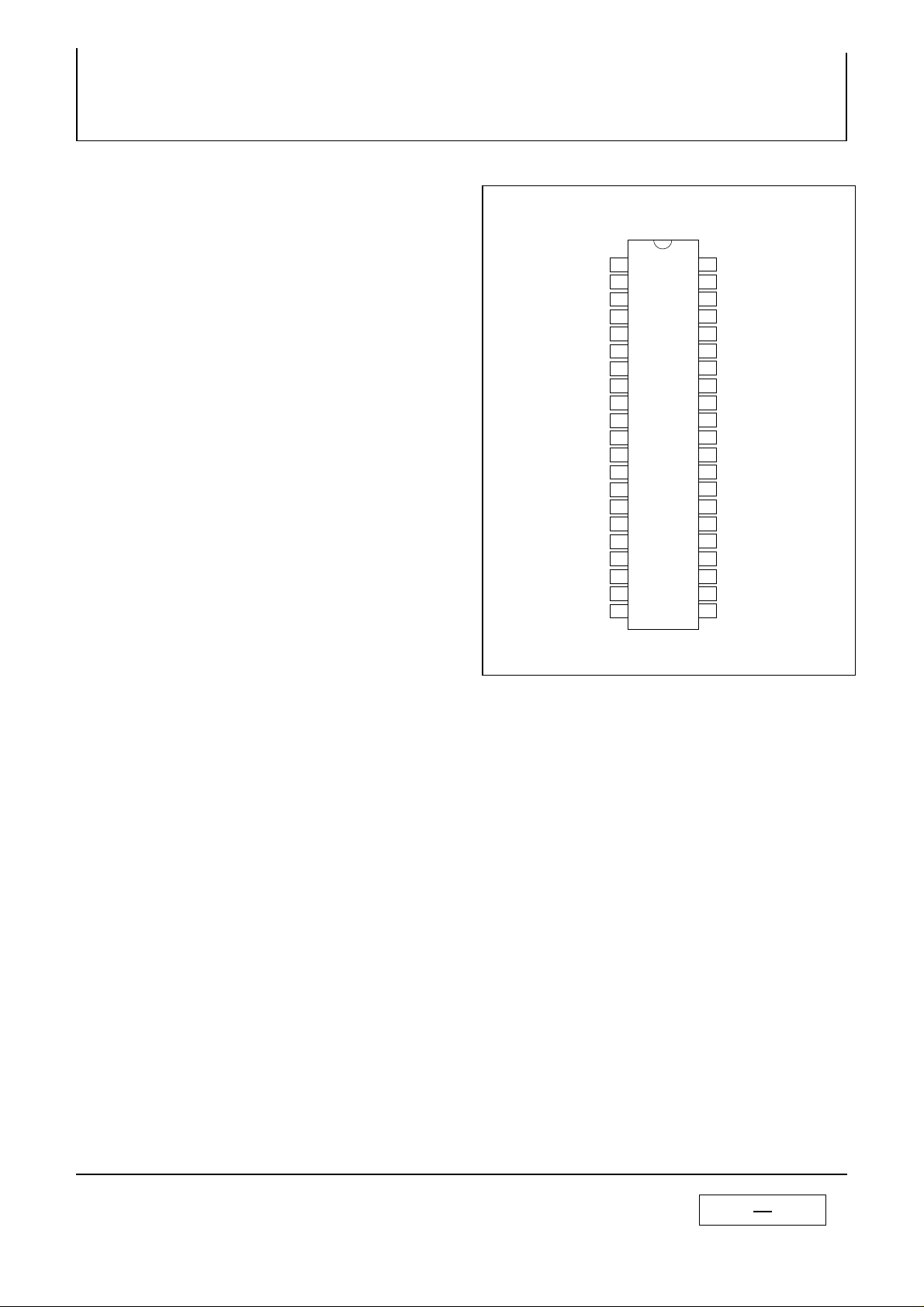
PIN CONFIGURATION
OSD BLK IN181
GND
NC
NC
2
3
4
5
6
7
8
9
10
11
12
13
14
15
16
17
19
20
21
INPUT(R)
VCC1(R)
OSD IN (R)
GND 1 (R)
INPUT(G)
INPUT(SOG)
VCC1 (G)
OSD IN (G)
GND 1 (G)
INPUT (B)
VCC1 (B)
OSD IN (B)
GND 1 (B)
ABL IN
VCC=5V
SOG Sep OUT
42
41
40
39
38
37
36
35
M52749FP
34
33
32
31
30
29
28
27
26
25
24
23
22
VCC 2
OUTPUT(R)
NC
GND 2
OUTPUT(G)
NC
GND
Contrast ref.
Main Brightness
OUTPUT(B)
GND
Contrast cont.
Retrace BLK IN
D/A OUT1
D/A OUT2
D/A OUT3
D/A OUT4
D/A OUT5
GND(5V)
SDA
SCLClamp Pulse IN
Package:42P9R
STRUCTURE
Bipolar Silicon Monolithic IC
APPLICATION
CRT Display Monitor
RECOMMENDED OPERATING CONDITIONS
Supply Voltage Range 11.5V~12.5V(V3,V8,V12,V42)
4.5V~5.5V(V19)
Rated Supply Voltage 12.0V(V3,V8,V12,V42)
5.0V(V19)
MAJOR SPECIFICATION
Bus Controlled 3ch Video Pre-Amp with OSD Mixing Function and Retrace Blanking Function
MITSUBISHI
251
Page 2
Fig. 1 Block Diagram
30
Retrace Blanking
34
Main Brightness
42
R OUTPUT
41
RETRACE
BLANKING
CLAMP
F/B
G OUTPUT
38
RETRACE
BLANKING
AMP
MITSUBISHI< LINEAR IC >
M52749FP
BUS CONTROLLED 3CH VIDEO PRE-AMP FOR CRT DISPLAY MONITOR
SCL
SDA
Vcc 5V
Cont
(DIGITAL)
23
19
I/F
BUS
DAC
22
24
26 27 28 29
DAC o u t p u t
25 393632
CLAMP
F/B
Main Contrast
B OUTPUT
35
33
RETRACE
BLANKING
AMP
Ref
Main Contrast
31
CLAMP
F/B
Vcc=12V
OSD MIX AMP
MAIN
CONTRAST
SUB
CONTRAST
CLAMP
OSD MIX
MAIN
CONTRAST
SUB
CONTRAST
CLAMP
OSD MIX
MAIN
CONTRAST
SUB
CONTRAST
CLAMP
4bit
OSD
LEVEL
Main
CONTRAST
8bit
Sync On
B SUB CONT 8bit
R SUB CONT 8bit
G SUB CONT 8bit
Sep
Green
1
OSD Blanking
14
21
Clamp Pulse IN
2
4
R OSD IN
R INPUT
5
3
R Vcc 12V
9
6
G OSD IN
G INPUT
MITSUBISHI
8
10
G Vcc 12V
11
13
B OSD IN
B INPUT
16
12
B Vcc 12V
7
17
G INPUT
Contrast(ABL) IN
20
SOG Sep OUT
2
25
Page 3
MITSUBISHI< LINEAR IC >
M52749FP
BUS CONTROLLED 3CH VIDEO PRE-AMP FOR CRT DISPLAY MONITOR
Absolute Maximum Rating (Ambient temperature: 25 C)
Parameter
Supply voltage(PIN3,8,12,42)
Supply voltage(PIN19)
Power dissipation
Ambient temperature
Storage temperature
Recommended supply12
Recommended supply5
voltage range12
voltage range5
Thermal Derating Curve
Symbol Rating Unit
Vcc 12
Vcc 5
Pd
Topr
Tstg
Vopr12
13.0
6.0 V
2900
-20~+75
-40~+150
12.0
Vopr5 5.0
Vopr'12
Vopr'5
11.5~12.5 (TYP 12.0)
4.5~5.5 (TYP 5.0)
V
mW
C
C
V
V
V
V
3200
2900
2800
2400
2000
1600
1200
800
400
Permissible power dissipation Pd (mW)
0
Å|20 25
0
50
8575100
attached board
125 150
Ambient temperatureTa( C)
MITSUBISHI
3
25
Page 4
BUS CONTROL TABLE
(1) Slave address:
D7 D6 D5 D4 D3 D2 D1 R/W
1 0 0 0 1 0 0 0 =88H
(2) Each function's sub address:
MITSUBISHI< LINEAR IC >
M52749FP
BUS CONTROLLED 3CH VIDEO PRE-AMP FOR CRT DISPLAY MONITOR
NO. function bit
1 Main contrast 8
2 Sub contrast R 8
3 Sub contrast G 8
4 Sub contrast B 8
5 OSD level 4
6 06H
7
8
9
10
D/A OUT1 8
D/A OUT2 8
D/A OUT3 8
D/A OUT4 8
sub
add.
00H
01H
02H
03H
04H
07H
08H
09H
0AHD/A OUT5 8
Data Byte(up:bit information down:preset)
D7 D6 D5 D4 D3 D2 D1 D0
A07 A06 A05 A04 A03 A02 A01 A00
0 1 0 0 0 0 0 0
A17 A16 A15 A14 A13 A12 A11 A10
1 0 0 0 0 0 0 0
A27 A26 A25 A24 A23 A22 A21 A20
1 0 0 0 0 0 0 0
A37 A36 A35 A34 A33 A32 A31 A30
1 0 0 0 0 0 0 0
- - - - A43 A42 A41 A40
0 0 0 0 1 0 0 0
A67 A66 A65 A64 A63 A62 A61 A60
1 0 0 0 0 0 0 0
A77 A76 A75 A74 A73 A72 A71 A70
1 0 0 0 0 0 0 0
A87 A86 A85 A84 A83 A82 A81 A80
1 0 0 0 0 0 0 0
A97 A96 A95 A94 A93 A92 A91 A90
1 0 0 0 0 0 0 0
AA7 AA6 AA5 AA4 AA3 AA2 AA1 AA0
1 0 0 0 0 0 0 0
MITSUBISHI
4
25
Page 5
2
I C BUS CONTROL SECTION
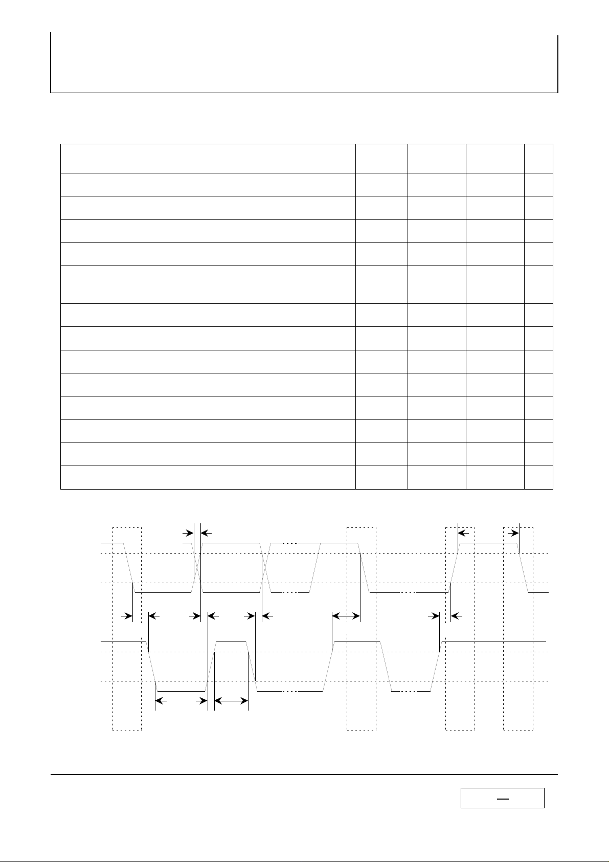
SDA,SCL CHARACTERISTICS
MITSUBISHI< LINEAR IC >
M52749FP
BUS CONTROLLED 3CH VIDEO PRE-AMP FOR CRT DISPLAY MONITOR
parameter symbol MIN MAX
min. input LOW voltage.
max. input HIGH voltage.
SCL clock frequency.
Time the bus must be free before a new transmission can start.
Hold time start condition.After this period the first clock pulse
is generated.
The LOW period of the clock.
The HIGH period of the clock.
Srt up time for start condition. (Only relevant for a repeated
start condition.)
Hold time DATA.
Set-up time DATA.
Rise time of both SDA and SCL lines.
VIL
VIH
fSCL
tBUF
tHD:STA
tLOW
tHIGH
tSU:STA
tHD:DAT
tSU:DAT
tR
-0.5 1.5 V
3.0 5.5 V
0 400 KHz
1.3
0.6
1.3
0.6
0.6
0.1
100
-
300
-
-
-
-
-
-
-
us
unit
us
us
us
us
us
ns
ns
Fall time of both SDA and SCL lines.
Set-up time for stop condition.
tR, tF
VIL
SDA
VIH
tHD:STA
VIL
SCL
VIH
tLOW
S S P S
tHIGH
tF
tSU:STO
0.6
-
300
-
ns
us
tBUF
tHD:DATtSU:DAT
tSU:STA
tSU:STO
MITSUBISHI
5
25
Page 6
Re-
mark
Note1
Note2
Note3
Note4
Note5
MITSUBISHI< LINEAR IC >
M52749FP
BUS CONTROLLED 3CH VIDEO PRE-AMP FOR CRT DISPLAY MONITOR
Note6
Note7
Note8
Note9
Note10
Note11
Note12
Note13
Note14
Note15
Note16
Unit
MAX
MIN TYP
0AH
D/A
OUT5
09H
D/A
OUT4
08H
D/A
OUT3
07H
D/A
OUT2
D/A
OUT1
04H 06H
OSD
BUS CTL (H )
Sub
cont
03H
Sub
cont
02H
Sub
cont
01H
00H
Main
17
CTL voltage
Adj
3
2
1
cont
FFH
FFH
FFH
FFH
FFH
00H
FFH
FFH
FFH
FFH
mA
130
110
-
255
255
255
255
255
0
255
255
255
255
5.0
4.0
mA
22
18
-
5.0
4.0
Vp-p
-
8.0
6.0
5.0
Variable
64H
Vp-p
-
-
1.6
100
5.0
2.0
dB
FFH
19.4
17.7
16.5
255
5.0
2.0
-
1.2
1.0
0.8
-
-
-
dB
C8H
15.5 17.0 18.5
200
5.0
2.0
-
1.2
1.0
0.8
-
dB
1.2
12.0
1.0
10.5
0.8
9.0
-
64H
-
-
100
5.0
2.0
-
14H
-
-
Vp-p
0.6
0.4
0.2
20
5.0
2.0
-
1.2
1.0
0.8
-
-
-
dB
C8H
C8H
C8H
FFH
15.5 17.0 18.5
200
200
200
255
5.0
2.0
-
1.2
1.0
0.8
-
-
-
-
-
-
dB
10.5
64H
64H
64H
FFH
13.5
12.0
100
100
100
255
2.0 5.0
-
1.2
1.0
0.8
-
-
-
-
-
-
aa
SG5
a
SG1
VC1
Main contrast
control relative
characteristics 1
7
8
-
-
a a
-
b
SG5
-
a
-
a
-
b
SG1
OUT
VC2
control
Main contrast
characteristics 1
9
-
-
-
-
-
-
-
VC2
Main contrast
control relative
characteristics 2
characteristics 2
10
a a
b
SG5
a
a
b
SG1
OUT
VC3
control
Main contrast
characteristics 3
11
-
-
-
-
-
-
-
VC3
Main contrast
control relative
characteristics3
12
a a
b
SG5
a
a
b
SG1
OUT
VSC1
control
Sub contrast
13
7
In
SOG
a a
a a
a a
a a
SG2
OUT
Vomax
range
3
a a
a a
b
SG2
Variable
IN
OUT
Vimax
Maximum input
4
b
30 34
ReT
BLK Bright
21
13
Input Standard
9
11 1 4
2 6
Test
Symbol
parameter
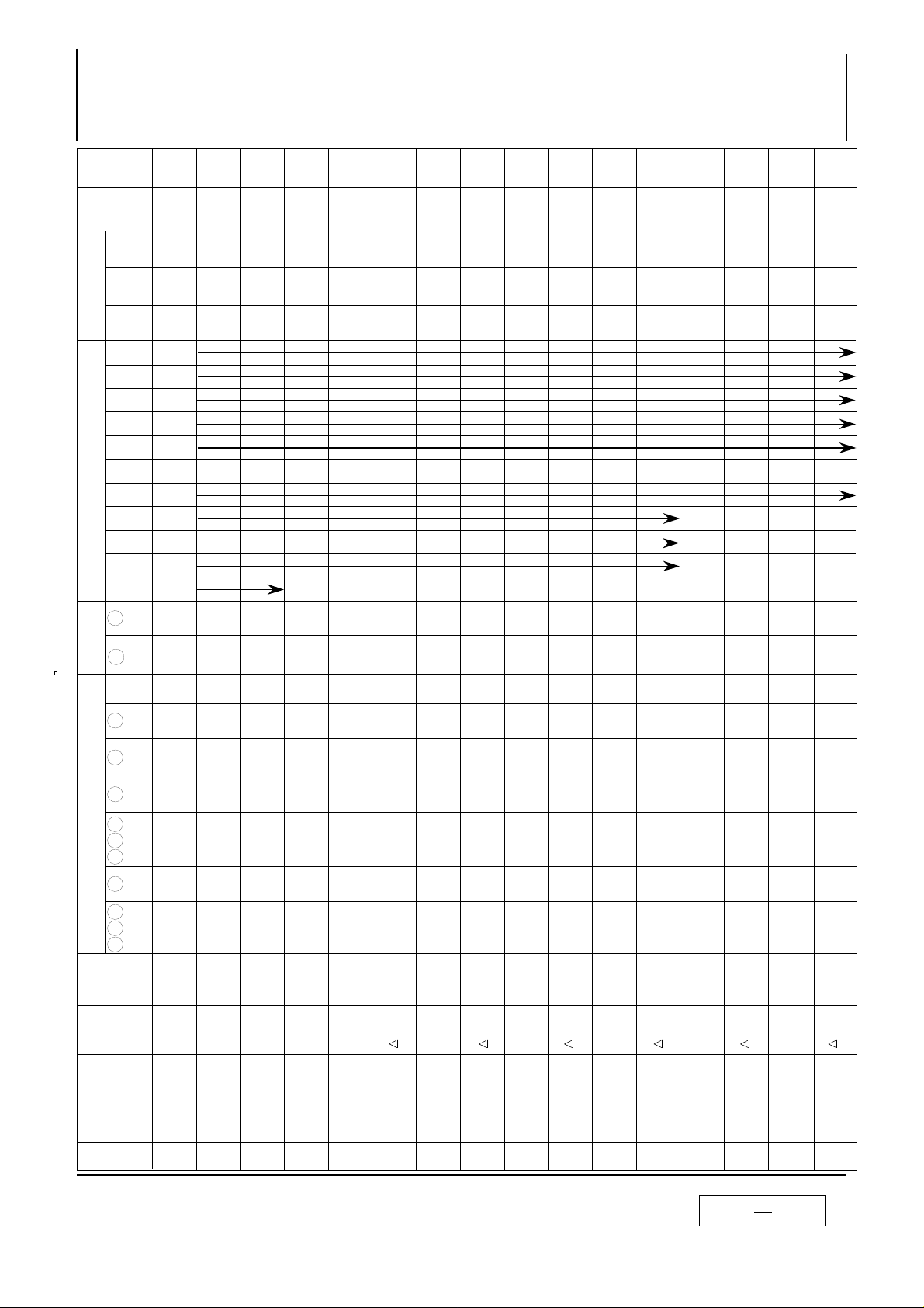
Supplementary Table1 Electrical Characteristics (Vcc = 12V,5V; Ta = 25C unless otherwise specified)
No
b
CP In
BLK ABL
OSD
RGB In OSD In
Point(s)
SG5bSG5bSG5bSG5bSG5
a a
a a
b
a
a
IA
IB
Icc1
Icc2
Output dynamic
Circuit current2
Circuit current1
1
2
-
-
a a
-
-
-
a a
-
SG1
-
OUT
Gv
Gv
Relative maximum
Maximum gain
6
5
gain
b
a
b
OUT
VC1
control
Main contrast
-
-
-
-
-
-
-
VSC1
Sub contrast
control relative
characteristics 1
characteristics 1
14
a a
b
SG5
a
a
b
SG1
OUT
VSC2
control
Sub contrast
characteristics 2
15
-
-
-
-
-
-
-
VSC2
Sub contrast
control relative
characteristics 2
16
MITSUBISHI
256
Page 7
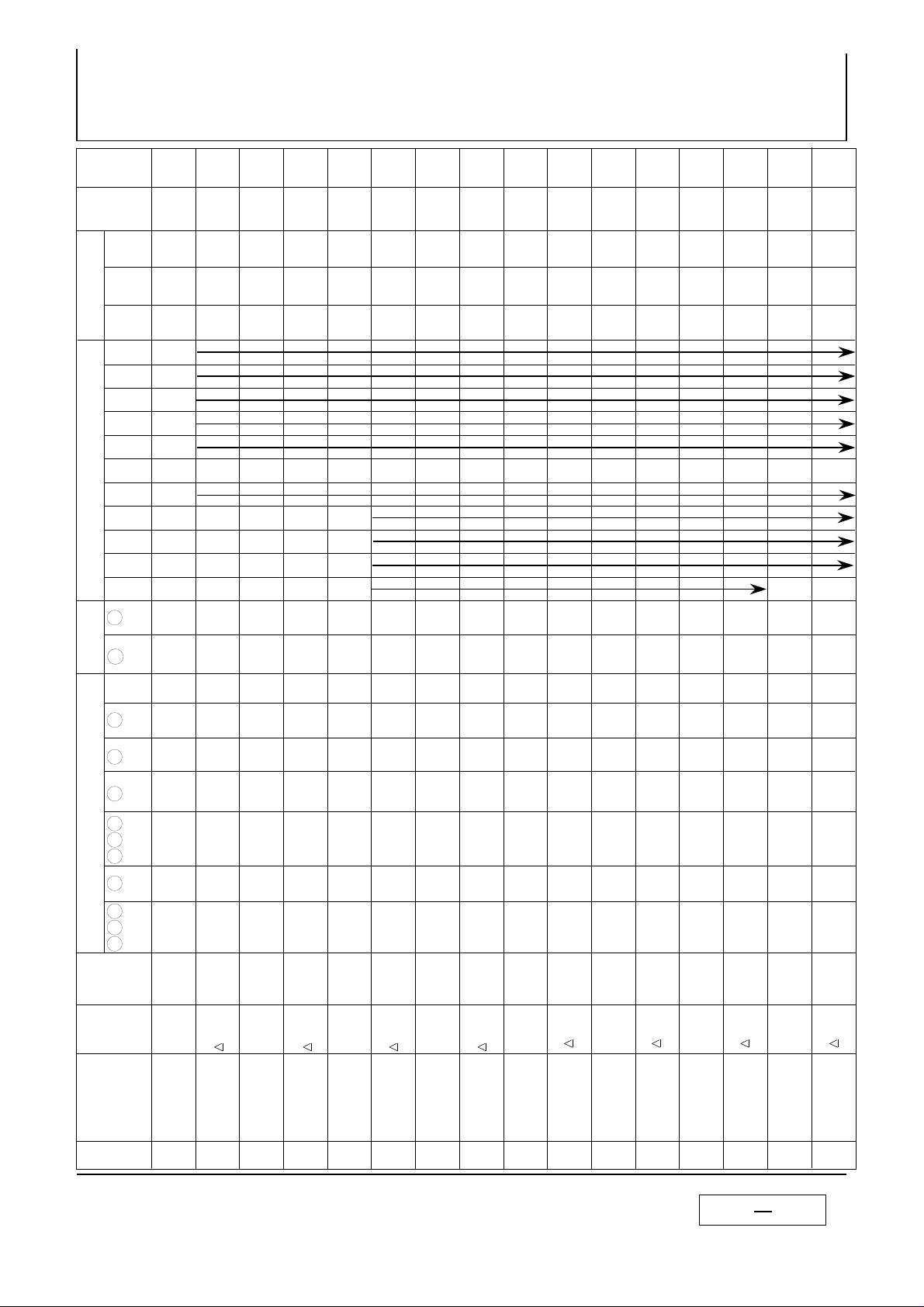
Re-
mark
Unit
Note17
Note18
-
Note19
Vp-p
Note20
-
Note21
MITSUBISHI< LINEAR IC >
M52749FP
BUS CONTROLLED 3CH VIDEO PRE-AMP FOR CRT DISPLAY MONITOR
Note22
Note23
Note24
-
-
Vp-p
Note25
V
Note26
V
Note27
V
Note28
V
Note29
V
Note30
V
Note31
dB
Note32
MAX
MIN TYP
0AH
D/A
OUT5
09H
D/A
OUT4
08H
D/A
OUT3
07H
D/A
OUT2
D/A
OUT1
04H 06H
OSD
BUS CTL (H )
Sub
cont
03H
Sub
cont
02H
Sub
cont
01H
00H
Main
17
CTL voltage
FFH
FFH
FFH
FFH
FFH
Adj
00H
3
14H
2
14H
1
14H
cont
FFH
Bright
0.7 1.2 1.5 Vp-p
255
255
255
255
255
0
20
20
20
255
5.0
2.0
1.2
0.8 1.0
-
-
-
-
-
-
C8H
C8H
C8H
C8H
4.03.4 4.6
200
200
200
200
5.0OUT
2.0
1.2
0.8 1.0
-
-
-
-
-
-
FFH
FFH
FFH
FFH
4.6 5.4 6.2 Vp-p
255
255
255
255
2.0 4.0
1.2
0.8 1.0
-
-
2.3 2.8 3.3
2.0
2.0
1.2
0.8 1.0
-
-
3.6 4.0 4.4
5.0OUT
4.0
-0.3 0 0.3
-
-
1.8 2.1 2.4
5.0OUT
2.0
-0.3 0 0.3
-
-
0.9 1.1 1.3
5.0OUT
1.0
-0.3 0 0.3
-
-
2.5
0
-2.0
Vari
able
5.0OUT
Variable
-1.0 0 1.0 dB
-
-
-
7
SOG
30 34
ReT
21
13
Input Standard
9
OSD
11 1 4
2 6
Test
Point(s)
Symbol
parameter
No
In
a
a
BLK
b
CP In
a
a
BLK ABL
b
RGB In OSD In
OUT
VSC3
control
Sub contrast
17
SG5
--- - - --
SG1
VSC3
Sub contrast
control relative
characteristics 3
18
a
a
b
SG5
a
a
b
SG1
VMSC
control
characteristics
characteristics 3
Main/sub contrast
19
a
a
b
--- - - --
a
a
b
OUT
ABL1
VMSC
ABL control
characteristics
control relative
Main/sub contrast
20
21
SG5
--- - - --
SG1
ABL1
characteristics 1
characteristics 1
ABL control relative
22
a
a
b
SG5
a
a
b
SG1
OUT
ABL2
ABL control
characteristics 2
23
a
a
b
SG5
--- - - --
a
a
a
VB1
ABL2
characteristics2
characteristics 1
Brightness control
ABL control relative
24
25
a
a
b
SG5
--- - - --
a
a
a
VB2
VB1
relative
characteristics 1
Brightness control
26
Brightness control
27
--- - - --
VB2
relative
characteristics 2
characteristics 2
Brightness control
28
a
a
b
SG5
--- - - --
a a
a
VB3
VB3
relative
characteristics 3
Brightness control
Brightness control
29
30
a
a
a
5V
a a
b
SG3
FC1
Frequency
(f=50MHz)
characteristics 3
characteristics 1
31
--
-
--
- -
FC1
(f=50MHz)
characteristics 1
Frequency relative
32
MITSUBISHI
257
Page 8
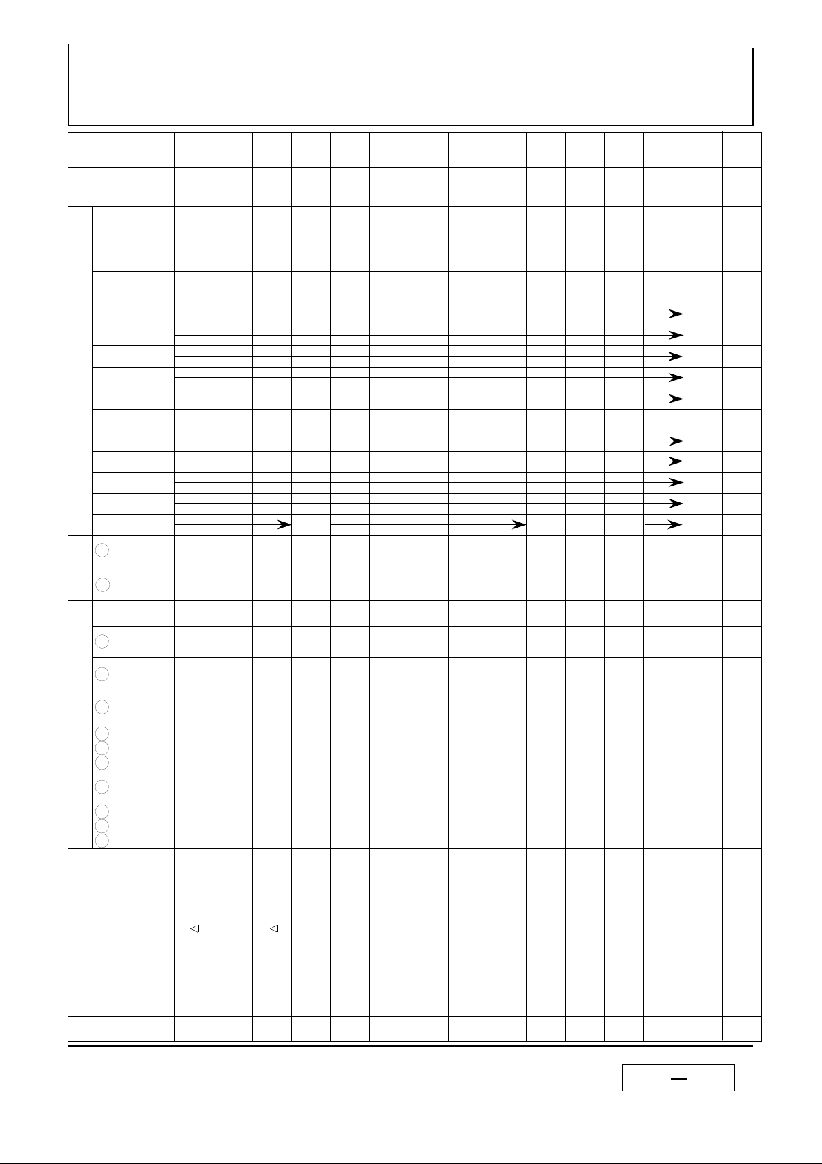
Re-
mark
Note33
Note34
Note35
Note36
Note37
MITSUBISHI< LINEAR IC >
M52749FP
BUS CONTROLLED 3CH VIDEO PRE-AMP FOR CRT DISPLAY MONITOR
Note38
Note39
Note40
Note41
Note42
Note43
Note44
Note45
Note46
Unit
MAX
Standard
MIN TYP
0AH
D/A
OUT5
09H
D/A
OUT4
08H
D/A
OUT3
07H
D/A
OUT2
D/A
OUT1
04H 06H
OSD
BUS CTL (H )
Sub
cont
3
03H
Sub
cont
2
02H
Sub
cont
1
01H
00H
Main
17
CTL voltage
FFH
FFH
FFH
FFH
FFH
00H
Adj
FFH
FFH
FFH
Vari
cont
Bright
dB
-3.0 0 3.0
255
255
255
255
255
0
255
255
255
able
5.0
Variable
dB
-1.0 0 1.0dB-3.0 3.0 5.0dB-1.0 0 1.0
-
5.0
-
Variable
- -
dB
-25 -20
-
255
FFH
5.0
Variable
dB
-20 -15
-
5.0
Variable
dB
-25 -20
-
5.0
Variable
dB
-20 -15
-
5.0
Variable
dB
-25 -20dB-20 -15
-
-
5.0
5.0
Variable
Variable
nS
2.8
2.0
-
Vari
able
5.0
Variable
nS
2.8
2.0
-
Vari
able
5.0
Variable
1.0 1.5 2.0
FFH
V
255
5.0
2.0
uS
-
-
0.2
5.0
2.0
7
30 34
21
13
Input
9
11 1 4
2 6
Test
Symbol
parameter
No
In
SOG
ReT
BLK
a
CP In
BLK ABL
OSD
b
RGB In OSD In
Point(s)
Frequency
-
a
-
a
-
5V
- -
a a
-
SG3
-
OUT
FC1'
FC1'
(f=180MHz)
characteristics 1
characteristics 1
Frequency relative
33
34
a
a
a
a a
b
OUT
FC2
Frequency
(f=180MHz)
characteristics 2
35
5V
SG3
(f=180MHz)
characteristics 2
Frequency relative
-
-
-
- -
-
-
FC2
(f=180MHz)
36
a
a
a
a
a
5Va5Va5Va5Va5Va5V
a
a
a a
2 b SG3
6 a
11a
OUT(33)
OUT(38)
CT1
(f=50MHz)
Crosstalk 1
37
2 b SG3
6 a
11a
OUT(33)
OUT(38)
CT1'
Crosstalk 1
(f=180MHz)
38
2 a
6 b SG3
OUT(33)
Crosstalk 2
a
a
aa
11a
OUT(41)
CT2
(f=50MHz)
39
a
a
a
a
2 a
6 b SG3
11a
OUT(33)
OUT(41)
CT2'
Crosstalk 2
(f=180MHz)
40
a
a
a a
2 a
6 a
11b SG3
OUT(38)
OUT(41)
CT3
(f=50MHz)
Crosstalk 3
41
a
a
a
a
2 a
6 a
11b SG3
OUT(38)
OUT(41)
CT3'
Crosstalk 3
(f=180MHz)
42
a
a
b
SG5bSG5
a a
b
SG1
OUT
Tr
Pulse
(3Vp-p)
characteristics 1
43
a
a
a
a
b
SG1
OUT
Tf
Pulse
(3Vp-p)
characteristics 2
44
a
a
b
SG5
Variable
a a
b
SG1bSG1
OUT
VthCP
Clamp pulse
threshold voltage
45
a
a
b
SG5
Variable
a
a
OUT
WCP
Clamp pulse
minimum width
46
MITSUBISHI
258
Page 9

Re-
Unit
mark
Note47
ns
Note48
ns
Note49
Vp-p
Note50
-
Note51
MITSUBISHI< LINEAR IC >
M52749FP
BUS CONTROLLED 3CH VIDEO PRE-AMP FOR CRT DISPLAY MONITOR
Note53
Note52
Vp-p
Note54
-
Note55
Note56
V
Note57
V
Note60
V
Note61
Vp-p
Note62
Vp-p-
MAX
MIN TYP
0AH
D/A
OUT5
09H
D/A
OUT4
08H
D/A
OUT3
07H
D/A
OUT2
D/A
OUT1
04H 06H
OSD
03H
02H
01H
00H
17
Sub
Sub
Sub
Main
cont
cont
cont
Adj
cont
Bright
BUS CTL (H )
CTL voltage
0.03
--
2.0 5.0
-
0.2
2.0 5.0
3.5
3.0 6.0
3.0 6.0
-
-
255
FFH
255
FFH
255
FFH
255
FFH
255
FFH
8
08H
08H
3
255
FFH
2
255
FFH
1
255
FFH
255
FFH
2.0 5.0
8
2.0 5.0
0FH
2.8 4.2
15
2.0 5.0OUT
0.8 1.0 1.2
-
-
-
2.8 Vp-p
2.25 3.35
08H
2.0 5.0
1.5
0.8 1.0 1.2
1.2 1.8
0
-
8
00H
-
-
2.0 5.0OUT
0.8 1.0 1.2
-
-
-
2.2 2.7 3.2V2.2 2.7 3.2
8
08H
2.0 5.0
00H
0
2.0 5.0
0.3
- 0.6
2.0 5.0OUT
1.0 1.5 2.0
2.0 5.0
7
SOG
30 34
ReT
21
13
Input Standard
9
OSD
11 1 4
2 6
Test
Point(s)
Symbol
parameter
No
In
a a
BLK
b
SG5bSG5bSG5
b
SG6bSG6bSG6
a
BLK ABL
a
RGB In OSD In CP In
OUT
OTr
OSD pulse
characteristics 1
47
a a
b
a
a
OUT
OTf
OSD pulse
characteristics 2
48
-
a
-
a
-
- -
SG6
-
a
-
Oaj1
Oaj1
relative
characteristics 1
OSD adjust control
49
characteristics 1
OSD adjust control
50
-
-
a a
b
b
b
OSD adjust control
-
SG5
-
SG6
-
SG6
-
a
-
OUT
Oaj2
Oaj2
relative
characteristics 2
OSD adjust control
51
52
a
a
b
SG5
b
SG6
b
SG6
a
Oaj3
characteristics 2
characteristics 3
OSD adjust control
53
-
a
-
a
-
b
SG5
-
b
SG6
-
b
SG6
-
a
OUT
Oaj3
VthOSD
relative
OSD input
characteristics 3
OSD adjust control
54
55
a a
b
SG5
a
Variable
b
SG6
Variable
b
SG1
OUT
VthBLK
OSD BLK input
threshold voltage
threshold voltage
56
a
b
SG7
b
SG5
a a
a
HBLK1
Retrace BLK
characteristics 1
57
a
b
b
SG7
Variable
b
SG5
a
a
a
OUT
SS -NVSS -
VthRET
SOG input
threshold voltag
Retrace BLK input
60
b
SG4
SG4
Variable
a
a
a
a
a
a
a a
a
a
SonG IN
SonG IN
SyncOUT
voltage
SOG minimum
maximum noise
61
62
Variable
SyncOUT
SV
input voltage
MITSUBISHI
259
Page 10

Re-
Unit
mark
MAX
Note63
Note64
Note65
Note66
Note67
VDC
MITSUBISHI< LINEAR IC >
M52749FP
BUS CONTROLLED 3CH VIDEO PRE-AMP FOR CRT DISPLAY MONITOR
Note68
VDC
Note69
mA
-
-
Note69a
mA
1.0
-
Note70
LSB
-
Standard
MIN TYP
D/A
OUT5
0AH
09H
D/A
OUT4
08H
D/A
OUT3
07H
D/A
OUT2
D/A
OUT1
04H 06H
OSD
BUS CTL (H )
Sub
cont
03H
Sub
cont
02H
Sub
cont
01H
00H
Main
17
CTL voltage
7
SOG
30 34
ReT
Adj
3
2
1
cont
Bright
In
BLK
b
4.5 4.9 5.0 V
2.0 5.0
SG4
a
4.5 5.0 5.5
255
255
255
255
255
0
255
255
255
255
2.0 5.0
a
a
00H
00H
00H
00H
00H
0 0.5 1.0
0
0
0
0
0
2.0 5.0
a
a
00H
00H
00H
00H
00H
00H
00H
00H
00H
00H
0 0.3 0.6 V
2.0 5.0
b
b
SG4
a
0 60 90 ns
0 60 90 ns
2.0 5.0
2.0 5.0
SG4bSG4
a
a
FFH
FFH
FFH
FFH
FFH
00H
FFH
FFH
FFH
FFH
0.18
0
0
0
0
0
0
0
0
0
0
2.0 5.0
a
a
-
2.0 5.0
-1.0 1.0
Vari
Vari
Vari
Vari
Vari
00H
FFH
FFH
FFH
FFH
able
able
able
able
able
0
255
255
255
255
2.0 5.0
a
a
21
13
Input
9
11 1 4
2 6
Test
Symbol
parameter
No
CP In
OSD
BLK ABL
RGB In OSD In
Point(s)
a
a
a
a
a
a
a
a
OUT
Sync
Sync
VSH
Level
Sync Output Hi
Sync Output Lo
63
64
OUT
VSL
Level
a
a
a
a
a
a
a
a
OUT
Sync
Time1
Sync Output Delay
OUT
TDS-R
Time2
66
Sync
TDS-F
Sync Output Delay
65
a
a
a
a
a
D/AOUT
VOH
voltage
D/A H output
67
D/A L output
a
a
a
D/AOUT
VOL
voltage
68
a
a
a
a
D/AOUT
IA-
D/AOUT
input current
69
MITSUBISHI
aa a a a a
D/AOUT
IA+
D/AOUT
output current
69a
a
a
a
a
D/AOUT
DNL
D/A nonlinearity
70
2510
Page 11

MITSUBISHI< LINEAR IC >
M52749FP
BUS CONTROLLED 3CH VIDEO PRE-AMP FOR CRT DISPLAY MONITOR
Note1) Measuring conditions are as listed in supplementary Table. Measured with a current meter
at test point IA.
Note2) Measuring conditions are as listed in supplementary Table. Measured with a current meter
at test point IB.
Note3) Decrease V34 gradually, and measure the voltage when the bottom of waveform output is
distorted. The voltage is called VOL.
Next, increase V34 gradually, and measure the voltage when the top of waveform output is
distorted. The voltage is called VOH.
Voltagr Vomax is calculated by the equation below:
Vomax = VOH - VOL
(V)
VOH
5.0
Waveform output
VOL
0.0
Note4) Increase the input signal(SG2) amplitude gradually, starting from 700mVp-p. Measure the
amplitude of the input signal when the output signal starts becoming distorted.
Note5) Input SG1, and read the amplitude output at OUT(33,38,41). The amplitude is called
VOUT(33,38,41).Maximum gain GV is calculated by the equation below:
VOUT
GV=20 LOG (dB)
Note6) Relative maximum gain GV is calculated by the equation below:
GV=VOUT(33)/VOUT(38), VOUT(38)/VOUT(41), VOUT(41)/VOUT(33)
Note7) Measuring the amplitude output at OUT(33,38,41). The measured value is called VOUT(33,38,41).
Main contrast conrol characteristics VC1 is calculated by the equation below:
VC1=20 LOG (dB)
Note8) Relative characteristics VC1 is calculated by the equation below:
VC1=VOUT(33)/VOUT(38) , VOUT(38)/VOUT(41) , VOUT(41)/VOUT(33)
Note9) Measuring condition and procedure are the same as described in Note7.
Note10) Measuring condition and procedure are the same as described in Note8.
0.7
VOUT
0.7
Note11) Measuring the amplitude output at OUT(33,38,41). The measured value is called VOUT(33,38,41).
Note12) Measuring condition and procedure are the same as described in Note8.
MITSUBISHI
2511
Page 12

MITSUBISHI< LINEAR IC >
M52749FP
BUS CONTROLLED 3CH VIDEO PRE-AMP FOR CRT DISPLAY MONITOR
Note13) Measure the amplitude output at OUT(33,38,41). The measured value is called VOUT(33,38,41).
Sub contrast conrol characteristics VSC1 is calculated by the equation below:
VOUT
VSC1=20 LOG (dB)
Note14) Relative characteristics VSC1 is calculated by the equation below:
VSC1=VOUT(33)/VOUT(38) , VOUT(38)/VOUT(41) , VOUT(41)/VOUT(33)
Note15) Measuring condition and procedure are the same as described in Note13.
Note16) Measuring condition and procedure are the same as described in Note14.
Note17) Measure the amplitude output at OUT(33,38,41). The measured value is called VOUT(33,38,41).
Note18) Measuring condition and procedure are the same as described in Note14.
Note19) Measure the amplitude output at OUT(33,38,41). The measured value is called VMSC.
Note20) Relative characteristics VMSC is calculated by the equation below:
VMSC=VOUT(33)/VOUT(38) , VOUT(38)/VOUT(41) , VOUT(41)/VOUT(33)
0.7
Note21) Measure the amplitude output at OUT(33,38,41). The measured value is called VOUT(33,38,41),
and is treated as ABL1.
Note22) Relative characteristics ABL1 is calculated by the equation below:
ABL1=VOUT(33)/VOUT(38) , VOUT(38)/VOUT(41) , VOUT(41)/VOUT(33)
Note23) Measuring condition and procedure are the same as described in Note21.
Note24) Measuring condition and procedure are the same as described in Note22.
Note25) Measure the DC voltage at OUT(33,38,41) with a voltmeter. The measured value is called
VOUT(33,38,41), and is treated as VB1.
Note26) Relative characteristics VB1 is calculated by the difference in the output between the channels.
VB1=VOUT(33)Å|VOUT(38) , VOUT(38)Å|VOUT(41) , VOUT(41)Å|VOUT(33)
Note27) Measuring condition and procedure are the same as described in Note25.
Note28) Measuring condition and procedure are the same as described in Note26.
Note29) Measuring condition and procedure are the same as described in Note25.
Note30) Measuring condition and procedure are the same as described in Note26.
MITSUBISHI
2512
Page 13

MITSUBISHI< LINEAR IC >
M52749FP
BUS CONTROLLED 3CH VIDEO PRE-AMP FOR CRT DISPLAY MONITOR
Note31) First, SG3 to 1MHz is as input signal. Input a resister that is about 2KOhm to offer the voltage at
input pins(2,6,11) in order that the bottom of input signal is 2.5V.
Control the main contrast in order that the amplitude of sine wave output is 4.0Vp-p.
Control the brightness in order that the bottom of sine wave output is 2.0Vp-p.
By the same way, measure the output amplitude when SG3 to 50MHz is as input signal.
The measured value is called VOUT(33,38,41).
Frequency characteristics FC1(33,38,41) is calculated by the equation below:
VOUT Vp-p
FC1=20 LOG (dB)
output amplitude when inputted SG3(1MHz) : 4.0Vp-p
Note32) Relative characteristics FC1 is calculated by the difference in the output between the channels.
Note33) Measuring condition and procedure are the same as described in Note31,except SG3 to 180MHz.
Note34) Relative characteristics FC1' is calculated by the difference in the output between the channels.
Note35) SG3 to 1MHz is as input signal. Control the main contrast in order that the amplitude of sine wave
output is 1.0Vp-p.
By the same way, measure the output amplitude when SG3 to 150MHz is as input signal.
The measured value is called VOUT(33,38,41).
Frequency characteristics FC2(33,38,41) is calculated by the equation below:
VOUT Vp-p
FC2=20 LOG (dB)
output amplitude when inputted SG3(1MHz) : 4.0Vp-p
Note36) Relative characteristics FC2 is calculated by the difference in the output between the channels.
Note37) Input SG3 (50MHz) to pin2 only, and then measure the waveform amplitude output at
OUT(33,38,41).The measured value is called VOUT(33,38,41).
Crosstalk CT1 is calculated by the equation below:
CT1=20 LOG (dB)
Note38) Measuring condition and procedure are the same as described in Note37,except SG3 to 180MHz.
Note39) Input SG3 (50MHz) to pin6 only, and then measure the waveform amplitude output at
OUT(33,38,41).The measured value is called VOUT(33,38,41).
Crosstalk CT2 is calculated by the equation below:
CT2=20 LOG
Note40) Measuring condition and procedure are the same as described in Note39,except SG3 to 180MHz.
Note41) Input SG3 (50MHz) to pin11 only, and then measure the waveform amplitude output at
OUT(33,38,41).The measured value is called VOUT(33,38,41).
Crosstalk CT2 is calculated by the equation below:
CT3=20 LOG
Note42) Measuring condition and procedure are the same as described in Note41,except SG3 to 180MHz.
VOUT(33,38)
VOUT(41)
VOUT(33,41)
(dB)
VOUT(38)
VOUT(38,41)
(dB)
VOUT(33)
MITSUBISHI
2513
Page 14

MITSUBISHI< LINEAR IC >
M52749FP
BUS CONTROLLED 3CH VIDEO PRE-AMP FOR CRT DISPLAY MONITOR
Note43) Control the main contrast (00H) in order that the amplitude of output signal is 3.0Vp-p.
Control the brightness (V34) in order that the Black level of output signal is 2.0V.
Measure the time needed for the input pulse to rise from 10% to 90% (Tr1) and for the output
pulse to rise from 10% to 90% (Tr2) with an active probe.
Pulse characteristics Tr is calculated by the equations below :
Tr= (Tr2)-(Tr1) (nsec)
Note44) Measure the time needed for the input pulseto fall from 90% to 10% (Tf1) and for the output
pulse to fall from 90% to 10% (Tf2) with an active probe.
Pulse characteristics Tf is calculated by the equations below :
Tr= (Tf2)-(Tf1) (nsec)
100%
0%
Note45) Turn down the SG5 input level gradually from 5.0Vp-p, monitoring the waveform output.
Measure thetop level of input pulse when the output pedestal voltage turn decrease with unstable.
2 2
2 2
Tr1
or
Tr2
90%
10%
Tf1
or
Tf2
Note46) Decrease the SG5 pulse width gradually from 0.5us, monitoring the output. Measure the SG5
pulse width (a point of 1.5V) when the output pedestal voltage turndecrease with unstable.
MITSUBISHI
2514
Page 15

MITSUBISHI< LINEAR IC >
Measure the SG6 level when the output reaches 0V. The measured value is called VthOSD.
Note56) Confirm that output signal is being blanked by the SG6 at the time.
Monitoring to output signal, decreasing the level of SG6. Measure the top level of SG6 when the
blanking period is disappeared. The measured value is called VthBLK.
Note57) Measure the amplitude output is blanked by the SG7 at OUT(33,38,41). The measured value is
called VOUT(33,38,41), and is treated as HBLK1.
Note60) Confirm that output signal is being blanked by the SG7 at the time.
Monitoring to output signal, decreasing the level of SG7. Measure the top level of SG7 when the
blanking period is disappeared. The measured value is called VthRET.
M52749FP
BUS CONTROLLED 3CH VIDEO PRE-AMP FOR CRT DISPLAY MONITOR
Note47) Measure the time needed for the output pulse to rise from 10% to 90% (OTr) with an active probe.
Note48) Measure the time needed for the output pulse to fall from 90% to 10% (OTf) with an active probe.
Note49) Measure the amplitude output at OUT(33,38,41). The measured value is called VOUT(33,38,41),
and is treated as Oaj1.
Note50) Relative characteristics Oaj1 is calculated by the equation below:
Oaj1=VOUT(33)/VOUT(38)ÅAVOUT(38)/VOUT(41)ÅAVOUT(41)/VOUT(33)
Note51) Measuring condition and procedure are the same as described in Note49.
Note52) Measuring condition and procedure are the same as described in Note50.
Note53) Measuring condition and procedure are the same as described in Note49.
Note54) Measuring condition and procedure are the same as described in Note50.
Note55) Reduce the SG6 input level gradually, monitoring output.
MITSUBISHI
2515
Page 16

MITSUBISHI< LINEAR IC >
M52749FP
BUS CONTROLLED 3CH VIDEO PRE-AMP FOR CRT DISPLAY MONITOR
Note61) The sync's amplitude of SG4 be changed all white into all black, increase from 0Vp-p to 0.02Vp-p.
No pulse output permitted.
Note62) The sync's amplitude of SG4 be changed all white or all black, decrease from 0.3Vp-p to 0.2Vp-p.
Confirm no malfunction produced by noise.
Note63) Measure the high voltage at SyncOUT. The measured value is treated as VSH.
Note64) Measure the low voltage at SyncOUT. The measured value is treated as VSL.
Note65) SyncOUT becomes High with sink part of SG4.
Measure the time needed for the rear edge of SG4 sink to fall from 50% and for SyncOUT to rise
from 50% with an active prove. The measured value is treated as TDS-F ,less than 90nsec.
Note66) Measure the time needed for the rear edge of SG4 sink to rise from 50% and for SyncOUT to fall
from 50% with an active prove. The measured value is treated as TDS-R ,less than 90nsec.
SG4
Pedestal voltage
sync (50%)
SyncOUT
Note67) Measure the DC voltage at D/AOUT. The measured value is treated as VOH.
Note68) Measure the DC voltage at D/AOUT. The measured value is treated as VOL.
Note69) IA- is minimum input-current when input 1VDC to D/AOUT.
IA-
D/A OUT
Note69a) IA+ is maximum output-current from D/AOUT.
Note70) The difference of differential non- linearity of D/AOUT must be less than 1.0LSB.
A
1VDC
(50%)
TDS-RTDS-F
+
MITSUBISHI
2516
Page 17

BUS CONTROLLED 3CH VIDEO PRE-AMP FOR CRT DISPLAY MONITOR
SG No. INPUT SIGNAL
MITSUBISHI< LINEAR IC >
M52749FP
SG1
Video signal
(all white)
SG2
Video signal
(step wave)
SG3
Sine wave
(for freq. char.)
SG4
8us
33us
Pulse with amplirude of
0.7Vp-p (f=30KHz).
Video width of 25us. (75%)
0.7VPP
0.7VP-P
(Amplitude is variable.)
Sine wave amplitude of 0.7Vp-p.
f=1MHz,50MHz,180MHz(variable)
Video width of 25us. (75%)
0.7VPP
all white or all black
variable.
Videosignal
(all white,all black)
SG5
Clamp
pulse
SG6
OSD pulse
SG7
BLK pulse
5us
3us
0.5us
5us
5VTTL
Sync's amplitude
0.3VPP
is variable.
Pulse width and
amplitude are variable.
5VTTL
Amplitude is variable.
5VTTL
Amplitude is variable.
MITSUBISHI
f=30KHz
17
25
Page 18

TEST CIRCUIT
SCL
SDA
22
23
gnddacdac dac dac
MITSUBISHI< LINEAR IC >
M52749FP
BUS CONTROLLED 3CH VIDEO PRE-AMP FOR CRT DISPLAY MONITOR
c/p
sync
5V
21
20
19
C/P IN
47u
SW
SYNC
OUT
21
1K
a
SG5
b
IB
5V
A
SG7
D/A
D/A
D/A
D/A
D/A
V34
OUT5
OUT4
OUT3
OUT2
OUT1
0~5V
25 2436
26
27
dac
NCgnd
abl
NC
V17
0~5V
: MEASURE POINT
Capacitor:0.01uF(unless otherwise specified.)
29
b
30
SW
a
1K
1K
2.2u
30
31 28
32
33
35 34
37
3839
blk sclsda
C/CC/R
gndgnd
brt
NC
B osd
osdSonG gnd12V
12VG
gnd12V
100K
IN(11)
SONG
IN
IN(6)
0.01u
+
3.3u
0.01u3.3u
+
1u
SW13
SW11
SW9
SW7
SW6
SW4
a
b
a
b
a
b
a
b
a
b
a
b
SG4
OUT(41) OUT(38) OUT(33)
100
1K
100uH
41 40
42
NC
R osd gnd
12V out gnd out out
blk
MITSUBISHI
1 2 3 4 5 6 7 8 9 10 11 12 13 14 15 17 1816
IN(2)
0.01u
+
3.3u
SW1 SW2
SG1
SG2
b
a
b
a
IA
A
47u
+
18
SG3
SG6
12V
25
Page 19

Terminal Description
MITSUBISHI< LINEAR IC >
M52749FP
BUS CONTROLLED 3CH VIDEO PRE-AMP FOR CRT DISPLAY MONITOR
No.
1
2
6
11
Name
OSD BLK IN
INPUT (R)
INPUT (G)
INPUT (B)
DC
Voltage
(V)
2.5
peripheral Circuit
2K
1
2K 2K
0.3mA
Remark
Input pulses
R
G
B
Connected to GND if
2.7V
0.46mA
2.5V
CP
not used.
Clamped to about 2.5 V
due to clamp pulses
from pin 21.
Input at low impedance.
3.7~5V
1.7V~GND
12
13
5
10
14
16
24
32
36
39
3
8
4
9
VCC 1(R)
VCC 1(G)
VCC 1(B)
OSD IN (R)
OSD IN (G)
OSD IN (B)
GND1(R)
GND1(G)
GND
GND1(B)
GND(5V)
GND
GND
GND 2
12
GND
1K
2K
0.5mA
Apply equivalent
voltage to 3 channels.
Input pulses
3.7~5V
1.7V~GND
Connected to GND if
not used.
2.7V
MITSUBISHI
2519
Page 20

MITSUBISHI< LINEAR IC >
M52749FP
BUS CONTROLLED 3CH VIDEO PRE-AMP FOR CRT DISPLAY MONITOR
No.
7
17
Name
INPUT (S on G)
ABL IN
DC
Voltage
(V)
When
open
2.5V
When
open
2.5V
peripheral Circuit
19
7
0.22mA 0.15mA 0.22mA
20K
1.2K1.2K 30K
0.5mA
17
500
2.5V
Remark
SYNC ON VIDEO input pin .
Sync is negative .
input signal at Pin7, compare
with the reference voltage
of internal circuit in order to
3.33V
separate sync signal from
Sync on Green signal .
ABL(AutomaticBeamLimiter)
input pin.
Recommended voltage range
is 0 to 5V.
When ABL function is not used,
set to 5V.
15
18
37
40
19
NC
5VCC(5V)
Sync signal output pin,
20
Being of open collector output
type.
SonG Sep OUT20
MITSUBISHI
2520
Page 21

MITSUBISHI< LINEAR IC >
M52749FP
BUS CONTROLLED 3CH VIDEO PRE-AMP FOR CRT DISPLAY MONITOR
No.
21
22
Name peripheral Circuit
Voltage
(V)
DC
Clamp Pulse IN
SCL
21
50K
22
2K
41K
2.2V
0.15mA
19
3V
Remark
Input pulses
2.5~5V
0.5V~GND
Input at low impedance.
2
SCL of I CBUS
(Serialclockline)
VTH=2.3V
23
25
26
27
28
29
SDA
D/]A OUT
19
50K
23
2K
3V
SDA of I CBUS
(Serialdataline)
VTH=2.3V
2
D/A output pin.
Output voltage range is 0~5V.
Min input current is 0.18mA
when D/A output pin is 1V.
Max output current is 1.0mA.
MITSUBISHI
2521
Page 22

MITSUBISHI< LINEAR IC >
M52749FP
BUS CONTROLLED 3CH VIDEO PRE-AMP FOR CRT DISPLAY MONITOR
No.
30 Retrace BLK IN
31
35
Name peripheral Circuit
Main Contrast Cont
Main Contrast Ref
DC
Voltage
(V)
3.5~5.5
4.5
30K
15K
30
15K
15K
50K
31
80K
2.25V
Remark
Input pulses
R
G
B
Connected to GND
if not used.
Non-polar capacitance is
1919
10K
35
required between pin31 and
pin35.
2.5~5V
0.5V~GND
33 OUTPUT (B)
38
41
42
34
OUTPUT (G)
OUTPUT (R)
VCC 2 12
Main Brightness
Variable
A resistor is needed on
42
50
50
35K
34
the GND side.
Set discretionally to maximum
15 mA, depending on the
required driving capacity.
Used to supply power to
output emitter follower
only.
It is recommended that the
IC be used between pedestal
voltage 2V and 3V.
MITSUBISHI
2522
Page 23

Electrical Chracteristics
MITSUBISHI< LINEAR IC >
M52749FP
BUS CONTROLLED 3CH VIDEO PRE-AMP FOR CRT DISPLAY MONITOR
Main Contrast Control Characteristics
6
4
2
Output Amplitude (Vp-p)
Sub Contrast : MAX
0
00H
Main Contrast Control Data
Brightness Control Characteristics
6
4
FFH
Sub Contrast Control Characteristics
6
4
2
Output Amplitude (Vp-p)
0
00H
Sub Contrast Control Data
Main Contrast : MAX
ABL Characteristics
6
4
FFH
2
Output DC Voltage (VDC)
0
0
Brightness Control Voltage (VDC)
OSD Adjust Control Characteristics
6
4
2
Output Amplitude (Vp-p)
0
0H
OSD Adjust Control Data
FH
2
Output Amplitude (Vp-p)
Main Contrast : MAX
Sub Contrast : MAX
0
5
12
0
ABL Control Voltage (VDC)
Sync separate input min sync width
5
(Video Duty=75%)
8
Sync separate
normal operating range
Duty of sync width (%)
4
7
1u
IN
input amplitude (Vp-p)
0.50
MITSUBISHI
23
25
Page 24

BUS CONTROLLED 3CH VIDEO PRE-AMP FOR CRT DISPLAY MONITOR
Application Method for M52749SP
CLAMP PULSE INPUT
Clamp pulse width is recommended
above 15 KHz, 1.0 usec
above 30 KHz, 0.5 usec
above 64 KHz, 0.3 usec .
MITSUBISHI< LINEAR IC >
M52749FP
The clamp pulse circuit in ordinary set is a long round about way,
and beside high voltage, sometimes connected to external terminal,
it is very easy affected by large surge.
Therefore, the Fig. shown right is recommended.
Notice of application
Make the nearest distance between output pin and pull down resister.
Recommended pedestal voltage of IC output signal is 2V.
21
MITSUBISHI
24
25
Page 25

APPLICATION EXAMPLE
110V
MITSUBISHI< LINEAR IC >
M52749FP
BUS CONTROLLED 3CH VIDEO PRE-AMP FOR CRT DISPLAY MONITOR
CRT
CutOffAdj
DAC OUT X5
0~5V
0.01u
100
100uH
42 41 40 39 38 37 36 35 34 33 32 31 30 29 28 27 26 25 24 23 22
NC NC
2.2u
1K1K1K
0.01u
0.01u0.01u0.01u
M52749FP
1 2 3 4 5 6 7 8 9 10 11 12 13 14 15 16 17 18 19 20 21
100K
0.01u
+
47u
5VTTL
3.3u
0.01u
+
0.01u
+
47u
75
NC
5VTTL
NC
0.01u
5VTTL
3.3u
0.01u
75
0.01u
+
47u
5VTTL
3.3u
++
0.01u
75
+
1u
0.01u
BLK IN
(for retrace)
SDA SCL
1K
OSD IN (B)
OSD IN (G)
OSD IN (R)
BLK IN
(for OSD)
5VTTL
ClampPulse
IN
ABL IN
0~5V
SyncSep
OUT
12V
5V
INPUT
(R)
INPUT
(G)
+
SONG
INPUT
MITSUBISHI
INPUT
(B)
0.01u
25
+
47u
25
 Loading...