

Page 1
Integrated
Circuit
Systems, Inc.
ICS85357-11
4:1 OR 2:1, CR YSTA L OSCILLATOR-TO-3.3V
LVPECL / ECL M
UL TIPLEXER
GENERAL DESCRIPTION
,&6
HiPerClockS™
inputs. The device can support 10MHz - 25MHz parallel
resonant crystals by connecting external capacitors between
XTALIN/XTALOUT and ground. The select pins have
internal pulldown resistors and leaving one input
unconnected (pulled to logic low by the internal resistor) will
transform the device into a 2:1 multiplexer. The SEL1 lead is
the most significant line and the binary number applied to
the select pins will select the same numbered data input (i.e.,
00 selects XTALIN0/XT ALOUT0).
The ICS85357-11 is a 4:1 or 2:1, Crystal
Oscillator-to-3.3V LVPECL / ECL Multiplexer and
is a member of the HiPerClockS™ family of High
Performance Clock Solutions from ICS. The
ICS85357-11 has 4 selectable crystal
FEATURES
• 1 differential 3.3V LVPECL output
• 4:1 or 2:1 Crystal Oscillator Multiplexer
• Supports parallel resonant crystals with a frequency range
of 10MHz - 25MHz. The oscillator circuit is optimized for
parallel resonant mode, and will require external capacitance
• Maximum output frequency up to 25MHz
• LVCMOS SEL0 and SEL1 inputs have internal pulldown
resistors
• Part-to-part skew: 150ps (maximum)
• Propagation delay: 2ns (maximum)
• LVPECL mode operating voltage supply range:
= 3.135V to 3.465V , VEE = 0V
V
CC
• ECL mode operating voltage supply range:
= 0V , VEE = -3.135V to -3.465V
V
CC
• 0°C to 70°C ambient operating temperature
• Industrial temperature information available upon request
BLOCK DIAGRAM PIN ASSIGNMENT
VCC
XTALIN0
XTALOUT0
XTALIN0
XTALOUT0
XTALIN1
XTALOUT1
XTALIN2
XTALOUT2
XTALIN3
XTALOUT3
OSC
OSC
OSC
OSC
00
01
10
11
Q0
nQ0
SEL0SEL1
XTALIN1
XTALOUT1
XTALIN2
XTALOUT2
XTALIN3
XTALOUT3
V
EE
ICS85357-11
20-Lead TSSOP
4.40mm x 6.50mm x 0.92mm body package
20
1
19
2
18
3
17
4
16
5
15
6
14
7
13
8
12
9
11
10
G Package
T op View
V
CC
SEL1
SEL0
V
CC
Q0
nQ0
V
CC
nc
nc
V
EE
85357AG-11 www.icst.com/products/hiperclocks.html REV. A JULY 25, 2001
1
Page 2
Integrated
Circuit
Systems, Inc.
TABLE 1. PIN DESCRIPTIONS
rebmuNemaNepyTnoitpircseD
02,71,41,1V
20NILATXtupnI.tupnilatsyrctnanoserlellaraP
30TUOLATXtupnI.tupnilatsyrctnanoserlellaraP
41NILATXtupnI.tupnilatsyrctnanoserlellaraP
51TUOLATXtupnI.tupnilatsyrctnanoserlellaraP
62NILATXtupnI.tupnilatsyrctnanoserlellaraP
72TUOLATXtupnI.tupnilatsyrctnanoserlellaraP
83NILATXtupnI.tupnilatsyrctnanoserlellaraP
93TUOLATXtupnI.tupnilatsyrctnanoserlellaraP
11,01V
31,21cndesunU.tcennocoN
61,510Q,0QntuptuO.slevelecafretniLCEPVL.stuptuokcolclaitnereffiD
810LEStupnInwodlluP.slevelecafretniLTTVL/SOMCVL.tupnitceleskcolC
911LEStupnInwodlluP.slevelecafretniLTTVL/SOMCVL.tupnitceleskcolC
pulluP
:ETON
CC
EE
dna
ICS85357-11
4:1 OR 2:1, CRYSTAL OSCILLATOR-TO-3.3V
LVPECL / ECL M
rewoP.V3.3ottcennoC.snipylppusevitisoP
rewoP.dnuorgottcennoC.snipylppusevitageN
nwodlluP
UL TIPLEXER
.seulavlacipytrof,scitsiretcarahCniP,2elbaTeeS.srotsisertupnilanretniotsrefer
TABLE 2. PIN CHARACTERISTICS
lobmySretemaraPsnoitidnoCtseTmuminiMlacipyTmumixaMstinU
C
NI
R
PULLUP
R
NWODLLUP
ecnaticapaCtupnI1LES,0LES4Fp
rotsiseRpulluPtupnI 15KΩ
rotsiseRnwodlluPtupnI 15KΩ
TABLE 3A. CONTROL INPUT FUNCTION TABLE
stupnItuOkcolC
1LES0LESKLC
00 0TUOLATX,0NILATX
01 1TUOLATX,1NILATX
10 2TUOLATX,2NILATX
11 3TUOLATX,3NILATX
85357AG-11 www.icst.com/products/hiperclocks.html REV. A JULY 25, 2001
2
Page 3
Integrated
Circuit
Systems, Inc.
4:1 OR 2:1, CR YSTAL OSCILLA TOR-TO-3.3V
LVPECL / ECL M
ICS85357-11
UL TIPLEXER
ABSOLUTE MAXIMUM RATINGS
Supply Voltage, V
Inputs, V
I
Outputs, V
Package Thermal Impedance, θ
Storage T emperature, T
CC
O
JA
STG
Stresses beyond those listed under Absolute Maximum Ratings may cause permanent damage to the device. These ratings
are stress specifications only . Functional operation of product at these conditions or any conditions beyond those listed in the
DC Characteristics
or
AC Characteristics
ods may affect product reliability.
4.6V
-0.5V to VCC + 0.5V
-0.5V to VCC + 0.5V
73.2°C/W (0lfpm)
-65°C to 150°C
is not implied. Exposure to absolute maximum rating conditions for extended peri-
TABLE 4A. POWER SUPPLY DC CHARACTERISTICS, V
= 3.3V±5%, TA = 0°C TO 70°C
CC
lobmySretemaraPsnoitidnoCtseTmuminiMlacipyTmumixaMstinU
V
CC
I
EE
egatloVylppuSevitisoP531.33.3564.3V
tnerruCylppuSrewoP 05Am
TABLE 4B. LVCMOS / LVTTL DC CHARACTERISTICS, V
lobmySretemaraPsnoitidnoCtseTmuminiMlacipyTmumixaMstinU
V
HI
V
LI
I
HI
I
LI
TABLE 4C. LVPECL DC CHARACTERISTICS, V
lobmySretemaraPsnoitidnoCtseTmuminiMlacipyTmumixaMstinU
V
HO
V
LO
V
GNIWS
egatloVhgiHtupnI1LES,0LES2567.3V
egatloVwoLtupnI1LES,0LES3.0-8.0V
tnerruChgiHtupnI1LES,0LESV
tnerruCwoLtupnI1LES,0LESVCCV,V564.3=
= 3.3V±5%, TA=0°C TO 70°C
CC
1ETON;egatloVhgiHtuptuOV
1ETON;egatloVwoLtuptuOV
gniwSegatloVtuptuOkaeP-ot-kaeP6.058.0V
05htiwdetanimretstuptuO:1ETON Ω Vot
.V2-
CC
= 3.3V±5%, TA = 0°C TO 70°C
CC
V=
CC
NI
V564.3=051Aµ
V0=5-Aµ
NI
CC
CC
4.1-V
0.2-V
0.1-V
CC
7.1-V
CC
85357AG-11 www.icst.com/products/hiperclocks.html REV. A JULY 25, 2001
3
Page 4
Integrated
Circuit
Systems, Inc.
TABLE 5. CRYSTAL CHARACTERISTICS
retemaraPsnoitidnoCtseTmuminiMlacipyTmumixaMstinU
tuc/noitallicsOfoedoM tnanoseRlellaraP/latnemadnuF
ycneuqerF 0152zHM
ecnaticapaCtnuhS 7Fp
ecnatcudnIniPseireS 37Hn
egnaRerutarepmeTgnitarepO 007C°
ICS85357-11
4:1 OR 2:1, CRYSTAL OSCILLATOR-TO-3.3V
LVPECL / ECL M
)RSE(ecnatsiseRseireStnelaviuqE 0508
UL TIPLEXER
Ω
TABLE 6. AC CHARACTERISTICS, V
lobmySretemaraPsnoitidnoCtseTmuminiMlacipyTmumixaMstinU
f
XAM
t
DP
)pp(kst4,2ETON;wekStraP-ot-traP 051sp
t
R
t
F
cdo4,3ETON;elcyCytuDtuptuO 7435%
LOTcso3ETON;ecnareloTrotallicsOlatsyrC 02±mpp
.noitceSnoitacilppA
emiTesiRtuptuO%08ot%02003007sp
emiTllaFtuptuO%08ot%02003007sp
= 3.3V±5%, TA=0°C TO 70°C
CC
egnaRycneuqerFtuptuO 0152zHM
1ETON;yaleDnoitagaporP IJ zHM521 2sn
.esiwrehtodetonsselnuzHM52taderusaemsretemarapllA
.tniopgnissorctuptuolaitnereffidehtottniopgnissorctupnilaitnereffidehtmorfderusaeM:1ETON
.tupniLATXehtgnivirdrevoderusaeM
segatlovylppusemasehttagnitareposecivedtnereffidnostuptuoneewtebwekssadenifeD:2ETON
derusaemerastuptuoeht,ecivedhcaenostupnifoepytemasehtgnisU.snoitidnocdaollauqehtiwdna
.tupniLATXehtgnivirdrevoderusaeM.stniopssorclaitnereffidehtta
ehtni6erugiFotrefeR.slatsyrcFp81htiwlellarapniFp72=2CdnaFp22=1CgnisuderusaeM:3ETON
.56dradnatSCEDEJhtiwecnadroccanidenifedsiretemarapsihT:4ETON
85357AG-11 www.icst.com/products/hiperclocks.html REV. A JULY 25, 2001
4
Page 5
Integrated
Circuit
Systems, Inc.
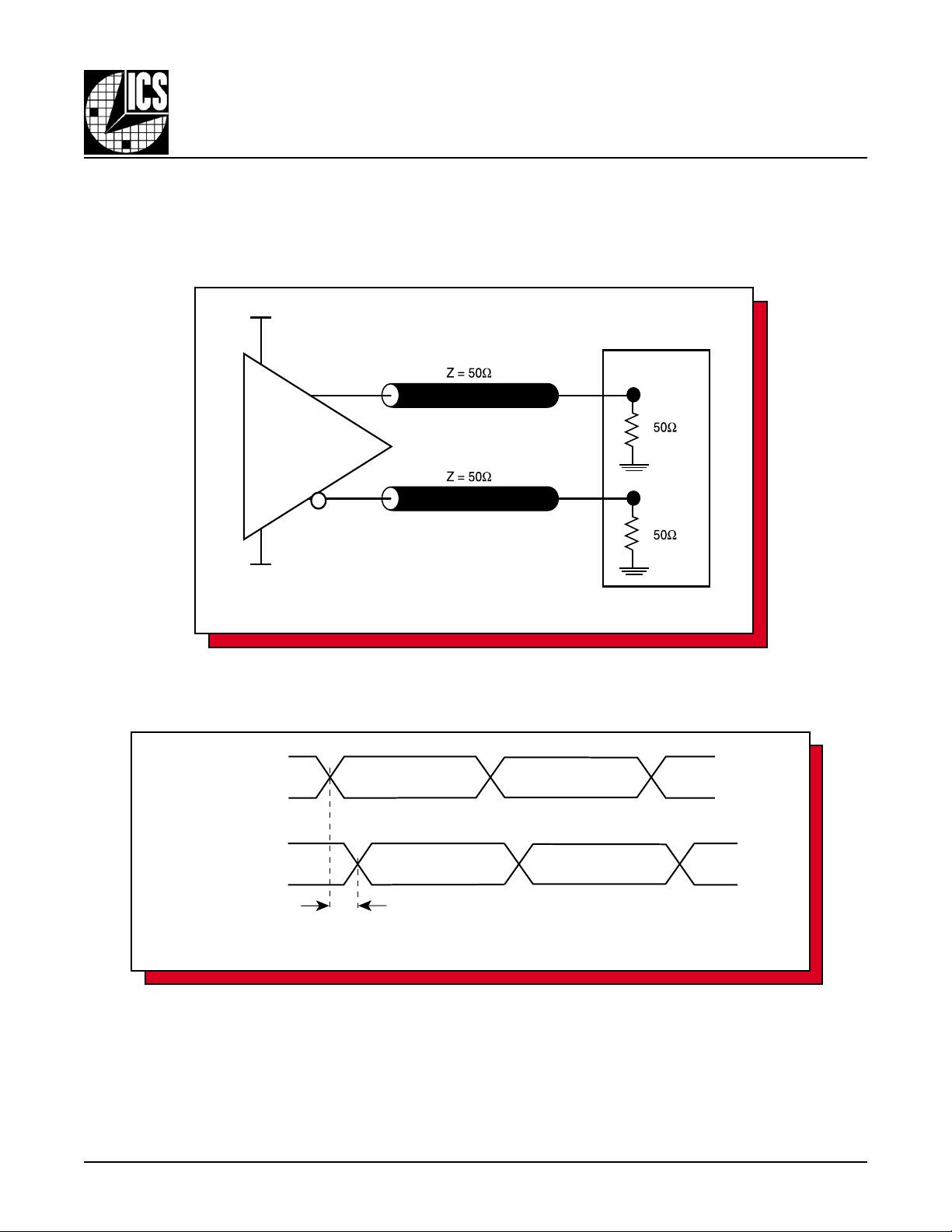
PARAMETER MEASUREMENT INFORMATION
V
CC
LVPECL
VCC = 2.0V
ICS85357-11
4:1 OR 2:1, CR YSTAL OSCILLA TOR-TO-3.3V
LVPECL / ECL M
SCOPE
Qx
nQx
UL TIPLEXER
VEE = -1.3V ± 0.135V
Q0
PART 1
nQ0
Q0
PART 2
nQ0
FIGURE 1 - OUTPUT LOAD TEST CIRCUIT
tsk(pp)
FIGURE 2 - PART-TO-PART SKEW
85357AG-11 www.icst.com/products/hiperclocks.html REV. A JULY 25, 2001
5
Page 6

Integrated
Circuit
Systems, Inc.
ICS85357-11
4:1 OR 2:1, CRYSTAL OSCILLATOR-TO-3.3V
LVPECL / ECL M
UL TIPLEXER
Clock Inputs
and Outputs
XTALINx
nQ0
Q0
80%
20%
t
R
t
F
FIGURE 3 - INPUT AND OUTPUT RISE AND FALL TIME
VCC/2
t
PD
80%
20%
V
SWING
Q0
nQ0
FIGURE 4 - P ROPAGATION DELAY
Pulse Width
t
PERIOD
t
odc =
PW
t
PERIOD
FIGURE 5 - odc & t
PERIOD
85357AG-11 www.icst.com/products/hiperclocks.html REV. A JULY 25, 2001
6
Page 7
Integrated
Circuit
Systems, Inc.
4:1 OR 2:1, CR YSTAL OSCILLA TOR-TO-3.3V
LVPECL / ECL M
ICS85357-11
UL TIPLEXER
APPLICA TION INFORMATION
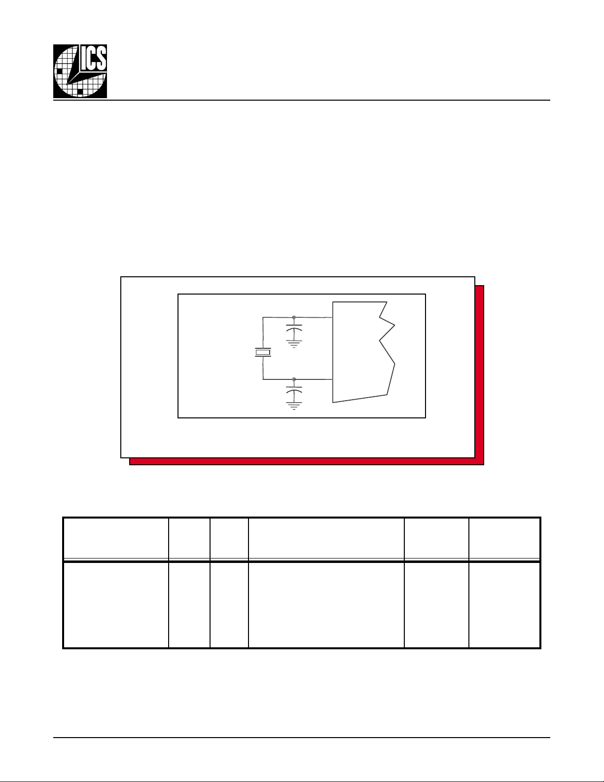
CRYSTA L INPUT INTERFACE
A crystal can be characterized for either series or parallel mode operation. The ICS85357-11 has a built-in crystal oscillator circuit.
This interface can accept either a series or parallel crystal without additional components and generate frequencies with accuracy
suitable for most applications. Additional accuracy can be achieved by adding two small capacitors C1 and C2 as shown in
Typical results using parallel 18pF crystals are shown in T able 7.
XTAL_IN
C1
22p
X1
18pF Parallel Crystal
XTAL_OUT
C2
27p
Figure 6
.
Figure 6. Crystal Input Interface
T able 7. Typical Results of Crystal Input Interface Frequency Fine Tuning
Crystal Frequency C 1 C2 Measured Output Frequency Accuracy Duty Cycle
(MHz) (pF) (pF) (MHz) (PPM) (%)
14.31818 22 27 14.318011 -12 47.46
15.00 22 27 14.999862 -9 47.70
16.66 22 27 16.660162 10 47.70
19.44 22 27 19.440081 4 46.85
24.00 22 27 24.000183 8 46.00
85357AG-11 www.icst.com/products/hiperclocks.html REV. A JULY 25, 2001
7
Page 8

Integrated
Circuit
Systems, Inc.
4:1 OR 2:1, CRYSTAL OSCILLATOR-TO-3.3V
LVPECL / ECL M
ICS85357-11
UL TIPLEXER
POWER CONSIDERATIONS
This section provides information on power dissipation and junction temperature for the ICS85357-11.
Equations and example calculations are also provided.
1. Power Dissipation.
The total power dissipation for the ICS85357-11 is the sum of the core power plus the power dissipated in the load(s).
The following is the power dissipation for V
NOTE: Please refer to Section 3 for details on calculating power dissipated in the load.
= 3.3V + 5% = 3.465V , which gives worst case results.
CC
• Power (core)
• Power (outputs)
Total Power
MAX
= V
MAX
_MAX
* I
CC_MAX
= 30.2mW/Loaded Output pair
= 3.465V * 50mA = 173.3mW
EE_MAX
(3.465V, with all outputs switching) = 173.3mW + 30.2mW = 203.5mW
2. Junction T emperature.
Junction temperature, Tj, is the temperature at the junction of the bond wire and bond pad and directly affects the reliability of the
device. The maximum recommended junction temperature for HiPerClockS
The equation for Tj is as follows: Tj = θ
Tj = Junction T emperature
θ
= junction-to-ambient thermal resistance
JA
Pd_total = T otal device power dissipation (example calculation is in section 1 above)
T
= Ambient T emperature
A
In order to calculate junction temperature, the appropriate junction-to-ambient thermal resistance θ
moderate air flow of 200 linear feet per minute and a multi-layer board, the appropriate value is 66.6°C/W per T able 6 below .
Therefore, Tj for an ambient temperature of 70°C with all outputs switching is:
70°C + 0.204W * 66.6°C/W = 83.6°C. This is well below the limit of 125°C
This calculation is only an example. Tj will obviously vary depending on the number of loaded outputs, supply voltage, air flow,
and the type of board (single layer or multi-layer).
* Pd_total + T
JA
A
TM
devices is 125°C.
must be used . Assuming a
JA
T able 8. Thermal Resistance qJA for 20-pin TSSOP, Forced Convection
q
by V elocity (Linear Feet per Minute)
JA
0 200 500
Single-Layer PCB, JEDEC Standard Test Boards 114.5°C/W 98.0°C/W 88.0°C/W
Multi-Layer PCB, JEDEC Standard Test Boards 73.2°C/W 66.6°C/W 63.5°C/W
NOTE: Most modern PCB designs use multi-layered boards. The data in the second row pertains to most designs.
85357AG-11 www.icst.com/products/hiperclocks.html REV. A JULY 25, 2001
8
Page 9
Integrated
Circuit
Systems, Inc.
4:1 OR 2:1, CR YSTAL OSCILLA TOR-TO-3.3V
LVPECL / ECL M
3. Calculations and Equations.
The purpose of this section is to derive the power dissipated into the load.
ICS85357-11
UL TIPLEXER
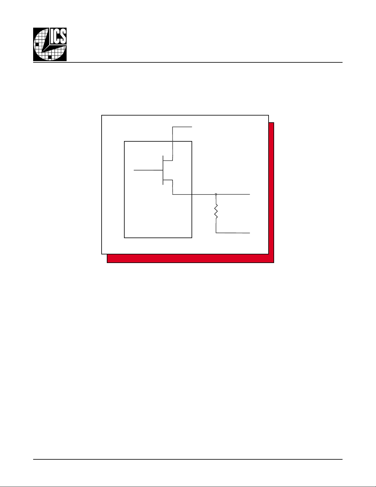
L VPECL output driver circuit and termination are shown in
VCC
Figure 7.
Q1
V
OUT
RL
50
V
- 2V
CC
FIGURE 7 - LVPECL DRIVER CIRCUIT AND TERMINATION
To calculate worst case power dissipation into the load, use the following equations which assume a 50Ω load, and a termination
voltage of V
Pd_H is power dissipation when the output drives high.
Pd_L is the power dissipation when the output drives low .
CC
- 2V .
Pd_H = [(V
Pd_L = [(V
• For logic high, V
Using V
• For logic low, V
Using V
OH_MAX
OL_MAX
– (V
– (V
CC_MAX
CC_MAX
- 2V))/RL] * (V
CC_MAX
- 2V))/RL] * (V
CC_MAX
= V
OUT
OH_MAX
= 3.465, this results in V
= V
OUT
OL_MAX
= 3.465, this results in V
= V
= V
CC_MAX
CC_MAX
CC_MAX
CC_MAX
- V
OH_MAX
- V
OL_MAX
– 1.0V
OH_MAX
– 1.7V
OL_MAX
)
)
= 2.465V
= 1.765V
Pd_H = [(2.465V - (3.465V - 2V))/50Ω] * (3.465V - 2.465V) = 20mW
Pd_L = [(1.765V - (3.465V - 2V))/50Ω] * (3.465V - 1.765V) = 10.2mW
T otal Power Dissipation per output pair = Pd_H + Pd_L = 30.2mW
85357AG-11 www.icst.com/products/hiperclocks.html REV. A JULY 25, 2001
9
Page 10

Integrated
Circuit
Systems, Inc.
4:1 OR 2:1, CRYSTAL OSCILLATOR-TO-3.3V
RELIABILITY INFORMATION
ICS85357-11
LVPECL / ECL M
UL TIPLEXER
TABLE 9. θ
TRANSISTOR COUNT
The transistor count for ICS85357-11 is: 413
VS
. AIR FLOW TABLE
JA
q
by V elocity (Linear Feet per Minute)
JA
0 200 500
Single-Layer PCB, JEDEC Standard Test Boards 114.5°C/W 98.0°C/W 88.0°C/W
Multi-Layer PCB, JEDEC Standard Test Boards 73.2°C/W 66.6°C/W 63.5°C/W
NOTE: Most modern PCB designs use multi-layered boards. The data in the second row pertains to most designs.
85357AG-11 www.icst.com/products/hiperclocks.html REV. A JULY 25, 2001
10
Page 11

Integrated
Circuit
Systems, Inc.
PACKAGE OUTLINE - G SUFFIX
ICS85357-11
4:1 OR 2:1, CR YSTAL OSCILLA TOR-TO-3.3V
LVPECL / ECL M
UL TIPLEXER
TABLE 10. PACKAGE DIMENSIONS
LOBMYS
N02
A--02.1
1A50.051.0
2A08.050.1
b91.003.0
c90.002.0
D04.606.6
ECISAB04.6
1E03.405.4
eCISAB56.0
L54.057.0
α
aaa--01.0
Reference Document: JEDEC Publication 95, MO-153
85357AG-11 www.icst.com/products/hiperclocks.html REV. A JULY 25, 2001
NIMXAM
°0 °8
11
sretemilliM
Page 12
Integrated
Circuit
Systems, Inc.
TABLE 11. ORDERING INFORMATION
rebmuNredrO/traPgnikraMegakcaPtnuoCerutarepmeT
11-GA75358SCI11GA75358SCIPOSSTdael02ebutrep27C°07otC°0
T11-GA75358SCI11GA75358SCIleeRdnaepaTnoPOSSTdael020052C°07otC°0
ICS85357-11
4:1 OR 2:1, CRYSTAL OSCILLATOR-TO-3.3V
LVPECL / ECL M
UL TIPLEXER
While the information presented herein has been checked for both accuracy and reliability, Integrated Circuit Systems, Incorporated (ICS) assumes no responsibility for either its use
or for infringement of any patents or other rights of third parties, which would result from its use. No other circuits, patents, or licenses are implied. This product is intended for use
in normal commercial applications. Any other applications such as those requiring extended temperature range, high reliability, or other extraordinary environmental requirements are
not recommended without additional processing by ICS. ICS reserves the right to change any circuitry or specifications without notice. ICS does not authorize or warrant any ICS
product for use in life support devices or critical medical instruments.
85357AG-11 www.icst.com/products/hiperclocks.html REV. A JULY 25, 2001
12
 Loading...