

Page 1
Features
•
Operating voltage: 2.7V ~5.5V
•
Low power consumption
–
Operation: 25mA Max. (VCC=5V)
10mA Max. (V
–
Standby: 30µA Max. (VCC=5V)
10
•
Access time:150ns Max. (VCC=5V)
µA Max. (V
250ns Max. (V
CC
CC
=3V)
CC
=3V)
=3V)
General Description
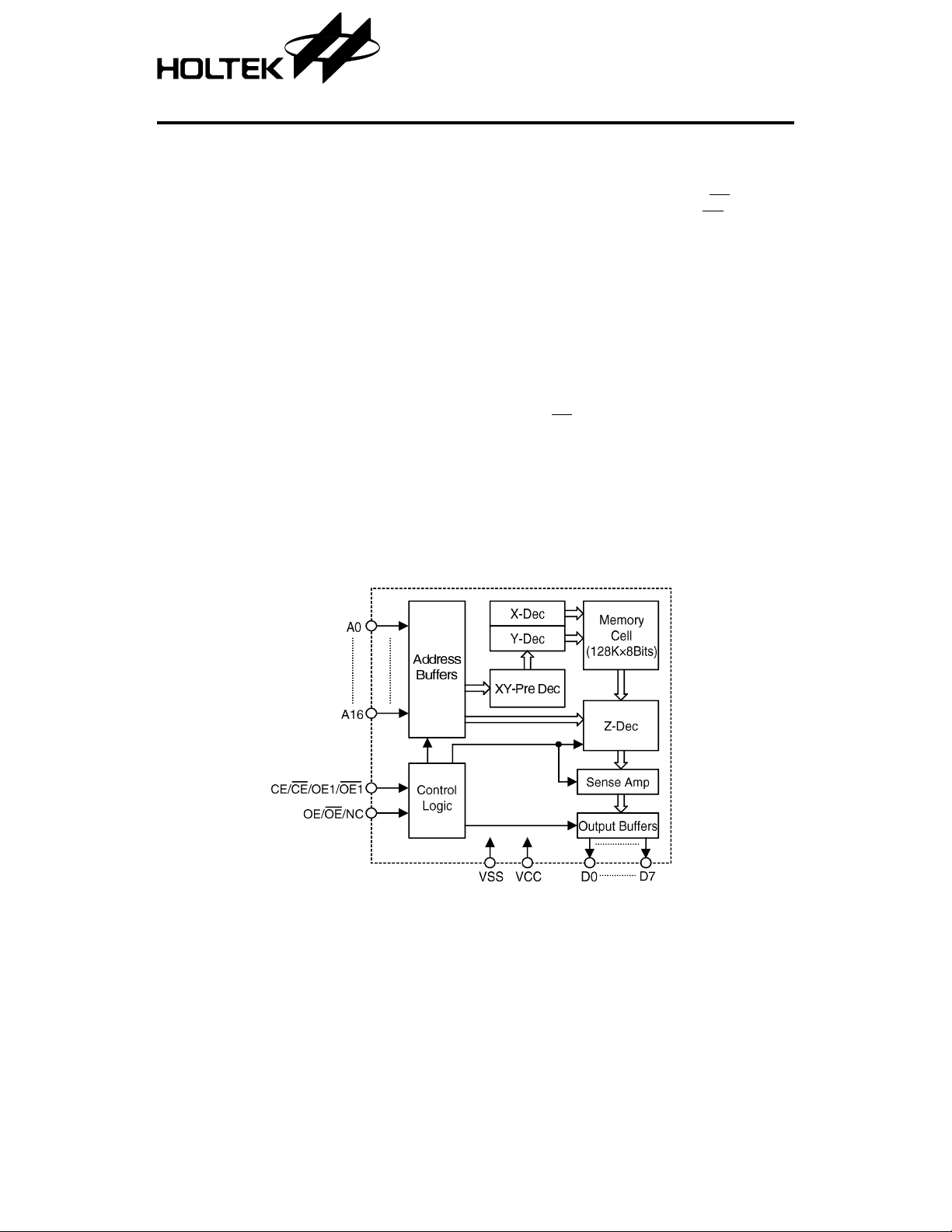
The HT23C010 is a read-only memory with
high performance CMOS storage device whose
1024K of memory is arranged into 131072
words by 8 bits.
For applica tion flexibility, the chip enable and
output enabl e control pins can be selected a s
active high or active low. This flexibility not
only allows easy interface with most microprocessors, but also eliminates bus contention in
HT23C010
CMOS 128K×8-Bit Mask ROM
•
131072×8 bits of mask ROM
•
Mask options: chip enable CE/CE/OE1/
OE1B and output enable OE/
•
TTL compatible inputs and outputs
•
Tristate outputs
•
Fully static operation
•
Package type: 28-pin DIP/SOP
32-pin DIP/SOP/PLCC
multiple bus mi cropro cessor syste ms. An add itional feature of the HT23C010 is its ability to
enter the standb y mode wh enever the chip enable (CE/
consumption to below 30
CE) is inactive, thus reducing current
µA. The combination of
these functions makes the chip suitable for high
density low power memory applications.
OE/NC
Block Diagram
1 24th Aug ’98
Page 2
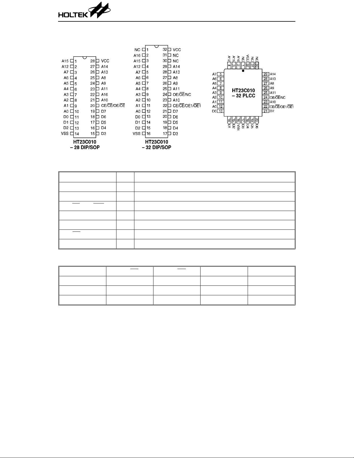
Pin Assignment
Pin Description
Pin Name I/O Description
HT23C010
A0~A16 I Address input s
D0~D7 O Data outputs
CE/
CE/OE1/OE1 I Chip enable output enable input
VSS I Negative power supply
VCC I Positive power supply
OE/
OE/NC I Output enable input
NC — No connection
Operation Truth Table
Mode CE/CE OE/OE A0~A16 D0~D7
Read H/L H/L Valid Data Out
Deselect H/L L/H X High Z
Standby L/H X X High Z
Note: H=V
, L=VIL, X=VIH or V
IH
IL
2 24th Aug ’98
Page 3
HT23C010
Absolu te Maxim um Ratings *
Supply Voltage.................................–0.3V to 6V Storage Temperature.................–50°C to 125°C
Input Voltage........................–0.3V to V
*Note: These are stress ra tings on ly. Stresses exceeding the range specified under “Abso lute Maxi -
mum Ratings” ma y cause substantial damage to the device. Functional operation of this
device at other conditions beyond those listed in the specification is not implied and prolonged
exposure to extreme condition s may affect device reliability.
D.C. Characteristics
Supply voltage: 2.7V~3.6V Ta=–40°C to 85°C
+0.3V Operating Temperature...............–40°C to 85°C
CC
Symbol Pa ra meter
V
CC
I
CC
V
IL
V
IH
V
OL
V
OH
I
LI
I
LO
I
STB1
I
STB2
C
IN
C
OUT
Operating Voltage — — 2.7 — 3.6 V
Operating Current 3V
Input Low Voltage 3V — V
Input High Voltage 3V — 2.0 — V
Output Low Voltage 3V IOL=2.1mA — — 0.4 V
Output High Voltage 3V IOH=–0.4mA 2.4 — V
Input Leakage Current 3V VIN=0 to V
Output Leakage Current 3V V
Standby Current 3V
Standby Current 3V
Input Capacitance (See note) — f=1MHz — — 10 pF
Output Capacitance (See note) — f=1MHz — — 10 pF
Test Conditions
V
CC
Conditions
O/P Unload,
f=5MHz
=0 to V
OUT
CE=V
CE=V
≤0.2V
CE
CE≥VCC-0.2V
IL
IH
CC
Min. Typ. Max. Unit
——10mA
— 0.4 V
SS
——10µA
CC
——10µA
——500µA
——10
CC
CC
V
V
µA
Note: These parameters are periodically sampled but not 100% tested.
Supply voltage: 4.5V~5.5V Ta=–40°C to 85°C
Symbol Pa ra meter
V
CC
I
CC
Operating Voltage — — 4.5 — 5.5 V
Operating Current 5V
Test Conditions
V
CC
Conditions
O/P Unload,
f=5MHz
3 24th Aug ’98
Min. Typ. Max. Unit
——25mA
Page 4

HT23C010
Symbol Parameter
V
IL
V
IH
V
OL
V
OH
I
LI
I
LO
I
STB1
I
STB2
C
IN
C
OUT
Input Low Voltage 5V — V
Input High Voltage 5V — 2.2 — V
Output Low Voltage 5V IOL=3.2mA — — 0.4 V
Output High Voltage 5V IOH=–1mA 2.4 — V
Input Leakage Current 5V VIN=0 to V
Output Leakage Current 5V V
Standby Current 5V
Standby Current 5V
Input Capacitance (See note) — f=1MHz — — 10 pF
Output Capacitance (See note) — f=1MHz — — 10 pF
Test Conditions
V
CC
Conditions
=0 to V
OUT
CE=V
CE=V
≤0.2V
CE
CE≥VCC-0.2V
IL
IH
CC
Min. Typ. Max. Unit
— 0.8 V
SS
——10µA
CC
——10µA
— — 1.5 mA
——30
CC
CC
V
V
µA
Note: These parameters are periodically sampled but not 100% tested.
A.C. Characteristics Ta=–40°C to 85°C
V
=2.7V~3.6V VCC=4.5V~5.5V
Symbol Parameter
t
CYC
t
AA
t
ACE
t
AOE
t
OH
t
OD
t
OE
Cycle Time 250 — 150 — ns
Address Access Time — 250 — 150 ns
Chip Enable Access Time — 250 — 150 ns
Output Enable Access Time — 150 — 80 ns
Output Hold Time — — 10 — ns
Output Disable Time (See Note) — — — 70 ns
Output Enable Time (See Note) — — 10 — ns
CC
Min. Max. Min. Max.
Unit
Note: These parameters are periodically sampled but not 100% tested.
A.C. test conditions
Output load: see figure right
Input rise and fall time: 10ns
Input pulse levels : 0.4V to 2.4V (V
CC
=5V)
Input and output timing reference levels:
0.8V and 2.0V (V
1.5V (V
CC
=3V)
CC
=5V)
4 24th Aug ’98
Output load circuit
Page 5

Functional Description
The HT23C010 has two modes, namely data
read mode and standby mode, controlled by
CE/
CE/OE1/OE1 and OE/OE/NC inputs.
•
Standby mode
The HT23C010 offers lower current consump-
tion, controlled by the chip enable input
(CE/
CE). When a low/high level is applied to the
CE/CEB input regardless of the output enable
(OE/
OE/NC) states the chip will enter the
standby mode.
•
Data read mode
When both the chip enable (CE/
and the output enable (OE/
the chip is in data read mode. Otherwise,
active CE/
in deselect mode. The output will remain i n
Hi-Z state.
CE and inactive OE/OE/N C result
Timing Diagrams
•
Propagation delay due to address (CE/CE/OE1/OE1 and OE/OE are active)
HT23C010
CE/OE1/OE1)
OE/NC) are active,
•
Propagation delay due to chip and output enable (address valid)
5 24th Aug ’98
Page 6

Characteristic Curves
HT23C010
6 24th Aug ’98
Page 7

HT23C010
7 24th Aug ’98
Page 8

HT23C010 MASK ROM ORDERING SHEET
Custom:
Input Medium:
EPROM DISK File (Mail Address: romfile@holtek.com.tw) OTHER
HT23C010
User No. Type/Ref. Name Q’ty Check Sum
Control Pin and Package Form Option:
(a) I . 28 Pin Type Pin 20:
II. 32 Pin Type Pin 22:
Pin 24:
(b) Package For m:
(6) 32 PLCC
Companion User No.
Package Marking :
Delivery Date : Q’ty:
CUSTOM CONFIRMED BY :
(1) CE (2) CE (3) OE (4) OE
(1) CE (2) CE (3) OE1 (4) OE1
(1) OE (2) OE (3) NC
(1) Chip Form (2) 28 DIP (3) 28 SOP (4) 32 DIP (5) 32 SOP
Memory Address
Start End
(NAME, DATE, POSITION & CO. CHOP)
HOL TEK CONFI RMED BY:
(SALES) (SALES MANAGER)
8 24th Aug ’98
 Loading...