

Page 1
Isolated 15-bit A/D Converter
Technical Data
Features
• 12-bit Linearity
• 700 ns Conversion Time
(Pre-Trigger Mode 2)
• 5 Conversion Modes for
Resolution/Speed Trade-Off;
12-bit Effective Resolution
with 18 µs Signal Delay
(14-bit with 94 µs)
• Fast 3 µs Over-Range
Detection
• Serial I/O (SPI®, QSPI® and
Microwire® Compatible)
• ±200 mV Input Range with
Single 5 V Supply
• 1% Internal Reference
Voltage Matching
H
HCPL-7860
HCPL-0870, -7870
• Offset Calibration
• -40°C to +85°C Operating
Temperature Range
• 15 kV/µs Isolation Transient
Immunity
• Regulatory Approvals; UL,
CSA, VDE
DIGITAL CURRENT SENSOR
++
YYWW
HPx870
DIGITAL
INTERFACE IC
OUTPUT
DATA
MICRO-CONTROLLER
INPUT
CURRENT
ISOLATION
BOUNDARY
YYWW
HP7860
ISOLATED
MODULATOR
Hewlett-Packard’s Isolated A/D Converter delivers the reliability, small size, superior
isolation and over-temperature performance motor drive designers need to accurately
measure current at half the price of traditional solutions.
CAUTION: It is advised that normal static precautions be taken in handling and assembly of this component to
prevent damage and/or degradation which may be induced by ESD.
SPI and QSPI are trademarks of Motorola Corp.
Microwire is a trademark of National Semiconductor Inc.
1-260
5965-5255E
Page 2
Digital Current Sensing Circuit
As shown in Figure 1, using the
Isolated 2-chip A/D converter to
sense current can be as simple as
connecting a current-sensing
resistor, or shunt, to the input
and reading output data through
the 3-wire serial output interface.
By choosing the appropriate
shunt resistance, any range of
current can be monitored, from
less than 1 A to more than 100 A.
Even better performance can be
achieved by fully utilizing the
more advanced features of the
Isolated A/D converter, such as
the pre-trigger circuit which can
reduce conversion time to less
NON-ISOLATED
+ 5 V
than 1 µs, the fast over-range
detector for quickly detecting
short circuits, different conversion
modes giving various resolution/
speed trade-offs, offset calibration mode to eliminate initial
offset from measurements, and
an adjustable threshold detector
for detecting non-short circuit
overload conditions.
ISOLATED
+ 5 V
R
SHUNT
0.02
+
C1
0.1 µF
INPUT
CURRENT
Figure 1: Typical Application Circuit.
Product Overview
Description
The HCPL-7860 Isolated Modulator and the HCPL-x870 Digital
Interface IC together form an
isolated programmable two-chip
analog-to-digital converter. The
isolated modulator allows direct
measurement of motor phase
currents in power inverters while
the digital interface IC can be
programmed to optimize the
conversion speed and resolution
trade-off.
In operation, the HCPL-7860
Isolated Modulator (optocoupler
with 3750 V
stand voltage rating) converts a
dielectric with-
RMS
V
V
DD1
MCLK
IN+
MDAT
IN-
GND2
HCPL-7860
DD2
C2
0.1 µF
V
V
GND1
low-bandwidth analog input into
a high-speed one-bit data stream
by means of a sigma-delta (∑∆)
oversampling modulator. This
modulation provides for high
noise margins and excellent
immunity against isolation-mode
transients. The modulator data
and on-chip sampling clock are
encoded and transmitted across
the isolation boundary where they
are recovered and decoded into
separate high-speed clock and
data channels.
The Digital Interface IC converts
the single-bit data stream from
the Isolated Modulator into
fifteen-bit output words and
provides a serial output interface
CCLK V
CLAT CHAN
CDAT SCLK
MCLK1 SDAT
MDAT1 CS
MCLK2 THR1
MDAT2 OVR1
GND RESET
HCPL-x870
DD
3-WIRE
SERIAL
INTERFACE
+
C3
10 µF
that is compatible with SPI®,
QSPI®, and Microwire® protocols, allowing direct connection
to a microcontroller. The Digital
Interface IC is available in two
package styles: the HCPL-7870 is
in a 16-pin DIP package and the
HCPL-0870 is in a 300-mil wide
SO-16 surface-mount package.
Features of the Digital Interface
IC include five different conversion modes, three different pretrigger modes, offset calibration,
fast over-range detection, and
adjustable threshold detection.
Programmable features are configured via the Serial Configuration port. A second multiplexed
input is available to allow
measurements with a second
1-261
Page 3
isolated modulator without
additional hardware. Because the
two inputs are multiplexed, only
one conversion at a time can be
made and not all features are
available for the second channel.
The available features for both
channels are shown in the table
at right.
Functional Diagrams
ISOLATION
BOUNDARY
V
DD1
V
IN+
V
IN–
GND1
1
2
3
4
SIGMA-
DELTA
MOD./
ENCODE
DECODE
SHIELD
V
8
DD2
7
MCLK
6
MDAT
GND2
5
HCPL-x870 Digital Interface IC
Feature Channel #1 Channel #2
Conversion Mode ✓✓
Offset Calibration ✓✓
Pre-Trigger Mode ✓
Over-Range Detection ✓
Adjustable Threshold Detection ✓
CCLK
1
2
3
4
5
6
7
8
CONFIG.
INTER-
FACE
CH1
CH2
CON-
VERSION
INTER-
FACE
THRES-
HOLD
DETECT
&
RESET
CLAT
CDAT SCLK
MCLK1 SDAT
MDAT1
MCLK2
MDAT2 OVR1
GND RESET
V
16
DD
15
CHAN
14
13
CS
12
11
THR1
10
9
HCPL-7860 Isolated Modulator
HCPL-x870 Digital Interface IC
Pin Description, Isolated Modulator
Symbol Description Symbol Description
V
DD1
V
IN+
V
IN–
GND1 Input ground GND2 Output ground
Supply voltage input (4.5 V to 5.5 V) V
DD2
Supply voltage input (4.5 V to 5.5 V)
Positive input (± 200 mV MCLK Clock output (10 MHz typical)
recommended)
Negative input MDAT Serial data output
(normally connected to GND1)
1-262
Page 4

Pin Description, Digital Interface IC
Symbol Description
CCLK Clock input for the Serial Configuration
Interface (SCI). Serial Configuration
data is clocked in on the rising edge
of CCLK.
CLAT Latch input for the Serial Configuration
Interface (SCI). The last 8 data bits
clocked in on CDAT by CCLK are
latched into the appropriate
configuration register on the rising
edge of CLAT.
CDAT Data input for the Serial Configuration
Interface (SCI). Serial configuration
data is clocked in MSB first.
MCLK1 Channel 1 Isolated Modulator clock
input. Input Data on MDAT1 is clocked
in on the rising edge of MCLK1.
MDAT1 Channel 1 Isolated Modulator data
input.
MCLK2 Channel 2 Isolated Modulator clock
input. Input Data on MDAT2 is clocked
in on the rising edge of MCLK2.
MDAT2 Channel 2 Isolated Modulator data
input.
GND Digital ground.
Symbol Description
V
Supply voltage (4.5 V to 5.5 V).
DD
CHAN Channel select input. The input level on
CHAN determines which channel of
data is used during the next conversion
cycle. An input low selects channel 1,
a high selects channel 2.
SCLK Serial clock input. Serial data is clocked
out of SDAT on the falling edge of SCLK.
SDAT Serial data output. SDAT changes from
high impedance to a logic low output
at the start of a conversion cycle.
SDAT then goes high to indicate that
data is ready to be clocked out. SDAT
returns to a high-impedance state after
all data has been clocked out and CS
has been brought high.
CS Conversion start input. Conversion
begins on the falling edge of CS. CS
should remain low during the entire
conversion cycle and then be brought
high to conclude the cycle.
THR1 Continuous, programmable-threshold
detection for channel 1 input data. A
high level output on THR1 indicates
that the magnitude of the channel 1
input signal is beyond a user
programmable threshold level between
160 mV and 310 mV. This signal
continuously monitors channel 1
independent of the channel select
(CHAN) signal.
OVR1 High speed continuous over-range
detection for channel 1 input data. A
high level output on OVR1 indicates
that the magnitude of the channel 1
input is beyond full-scale. This signal
continuously monitors channel 1
independent of the CHAN signal.
RESET Master reset input. A logic high input
for at least 100 ns asynchronously
resets all configuration registers to
their default values and zeroes the
Offset Calibration registers.
1-263
Page 5
Isolated A/D Converter Performance
Electrical Specifications
Unless otherwise noted, all specifications are at V
specifications are at TA = 25°C and V
TA = -40°C to +85°C, V
DD1
= V
DD2
= V
DD1
DD2
= VDD = 4.5 to 5.5 V.
Parameter Symbol Min. Typ. Max. Units Test Conditions Fig. Note
STATIC CONVERTER CHARACTERISTICS
Resolution 15 bits 1
Integral Nonlinearity INL 6 30 LSB 3 2
Differential Nonlinearity DNL 1 LSB 3
Uncalibrated Input Offset V
OS
Offset Drift vs. Temperature dVOS/dT
Offset drift vs. V
DD1
Internal Reference Voltage V
dVOS/dV
REF
DD1
-1 1 2.5 mV V
A
Absolute Reference Voltage -4 4 % 6 5
Tolerance
Reference Voltage -1 1 % TA = 25°C.
Matching See Note 5
V
Drift vs. Temperature dV
REF
V
Drift vs. V
REF
DD1
dV
Full Scale Input Range -V
REF
REF
/dT
/dV
A
DD1
REF
Recommended Input -200 +200
Voltage Range
DYNAMIC CONVERTER CHARACTERISTICS
(Digital Interface IC is set to Conversion Mode 3.)
Signal-to-Noise Ratio SNR 62 73 dB V
Total Harmonic Distortion THD -67
Signal-to-(Noise SND 66
+ Distortion)
Effective Number of Bits ENOB 10 12 bits 8 7
Conversion Time t
Signal Delay t
Over-Range Detect Time t
Threshold Detect Time t
Signal Bandwidth BW 18 22 kHz 11 12
Isolation Transient CMR 15 20 kV/µsV
Immunity
C2
t
C1
t
C0
DSIG
OVR1
THR1
2.0 2.7 4.2 V
= -200 mV to +200 mV and V
IN+
= 0 V; all Typical
IN-
= VDD = 5 V; all Minimum/Maximum specifications are at
0.025 0.14 % 4
= 0 V 5
IN+
4 µV/°C4
0.7 mV/V
326 mV
190 ppm/°C
0.9 %
+V
REF
mV 6
= 35 Hz, 2,9
IN+
400 mV
(141 mV
pk-pk
rms
) sine
wave.
0.7 1.0 µs Pre-Trigger Mode 2 7, 8
18 22 Pre-Trigger Mode 1
14
37 44 Pre-Trigger Mode 0
18 22 10 9
= 0 to 400 mV 12 10
IN+
10 11
step waveform
= 1 kV 13
ISO
1-264
Page 6
Notes:
1. Resolution is defined as the total
number of output bits. The useable
accuracy of any A/D converter is a
function of its linearity and signal-tonoise ratio, rather than how many
total bits it has.
2. Integral nonlinearity is defined as
one-half the peak-to-peak deviation
of the best-fit line through the
transfer curve for V
+200 mV, expressed either as the
= -200 mV to
IN+
number of LSBs or as a percent of
measured input range (400 mV).
3. Differential nonlinearity is defined as
the deviation of the actual difference
from the ideal difference between
midpoints of successive output
codes, expressed in LSBs.
4. Data sheet value is the average
magnitude of the difference in offset
voltage from TA=25°C to
TA= -40°C, expressed in microvolts
per °C.
5. All units within each HCPL-7860
standard packaging increment (either
50 per tube or 1000 per reel) have an
Absolute Reference Voltage tolerance
of ±1%. An Absolute Reference
Voltage tolerance of ± 4% is
guaranteed between standard
packaging increments.
6. Beyond the full-scale input range the
output is either all zeroes or all ones.
7. The effective number of bits (or
effective resolution) is defined by the
equation ENOB = (SNR-1.76)/6.02
and represents the resolution of an
ideal, quantization-noise limited A/D
converter with the same SNR.
8. Conversion time is defined as the
time from when the convert start
signal CS is brought low to when
SDAT goes high, indicating that
output data is ready to be clocked
out. This can be as small as a few
cycles of the isolated modulator clock
and is determined by the frequency of
the isolated modulator clock and the
selected Conversion and Pre-Trigger
modes. For determining the true
signal delay characteristics of the A/D
converter for closed-loop phase
margin calculations, the signal delay
specification should be used.
9. Signal delay is defined as the effective delay of the input signal through
the Isolated A/D converter. It can be
measured by applying a -200 mV to
± 200 mV step at the input of modulator and adjusting the relative delay
of the convert start signal CS so that
the output of the converter is at midscale. The signal delay is the elapsed
time from when the step signal is
applied at the input to when output
data is ready at the end of the conversion cycle. The signal delay is the
most important specification for
determining the true signal delay
characteristics of the A/D converter
and should be used for determining
phase margins in closed-loop applications. The signal delay is determined
by the frequency of the modulator
clock and which Conversion Mode is
selected, and is independent of the
selected Pre-Trigger Mode and,
therefore, conversion time.
10. The minimum and maximum overrange detection time is determined by
the frequency of the channel 1 isolated modulator clock.
11. The minimum and maximum threshold detection time is determined by
the user-defined configuration of the
adjustable threshold detection circuit
and the frequency of the channel 1
isolated modulator clock. See the
Applications Information section for
further detail. The specified times
apply for the default configuration.
12. The signal bandwidth is the frequency
at which the magnitude of the output
signal has decreased 3 dB below its
low-frequency value. The signal
bandwidth is determined by the frequency of the modulator clock and
the selected Conversion Mode.
13. The isolation transient immunity (also
known as Common-Mode Rejection)
specifies the minimum rate-of-rise of
an isolation-mode signal applied
across the isolation boundary beyond
which the modulator clock or data
signals are corrupted.
75.0
V
= 4.5 V
DD1
= 5.0 V
74.5
74.0
SNR
73.5
73.0
72.5
-40 85040
V
DD1
V
= 5.5 V
DD1
-20
20 60
TEMPERATURE – °C
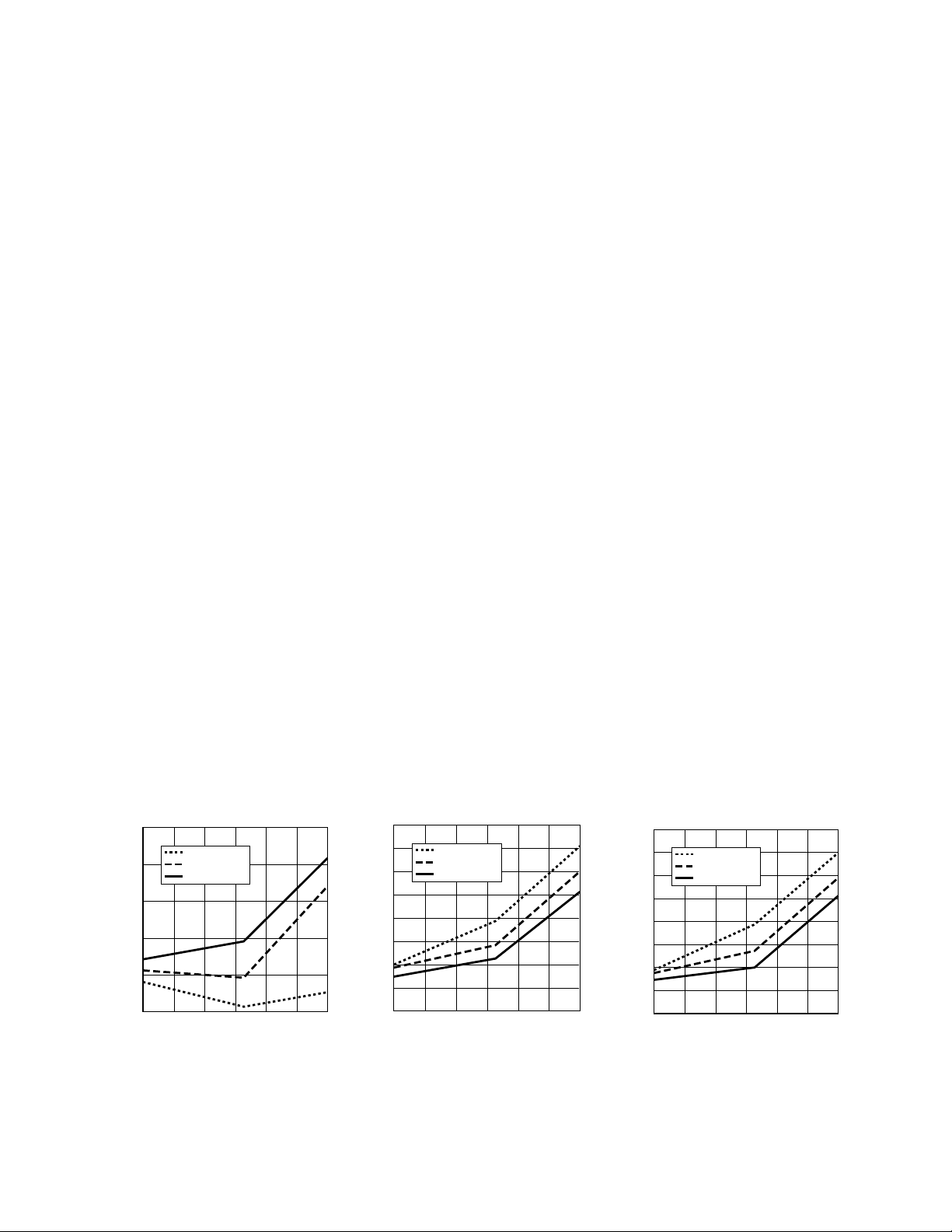
Figure 2. SNR vs. Temperature.
16
14
12
10
8
6
INL – LSB
4
2
0
-40 85040
V
= 4.5 V
DD1
= 5.0 V
V
DD1
V
= 5.5 V
DD1
-20
20 60
TEMPERATURE – °C
Figure 3. INL (Bits) vs. Temperature.
0.08
0.07
0.06
0.05
0.04
INL – %
0.03
0.02
0.01
0
-40 85040
V
= 4.5 V
DD1
= 5.0 V
V
DD1
V
= 5.5 V
DD1
-20
20 60
TEMPERATURE – °C
Figure 4. INL (%) vs. Temperature.
1-265
Page 7
400
300
200
100
0
-100
-200
-300
OFFSET CHANGE – µV
-400
-500
-600
-40 85
040
-20
TEMPERATURE – °C
V
DD1
V
DD1
V
DD1
20 60
= 4.5 V
= 5.0 V
= 5.5 V
2.5
2.0
1.5
1.0
0.5
CHANGE – %
0
REF
V
-0.5
-1.0
-1.5
-40 85040
V
= 4.5 V
DD1
= 5.0 V
V
DD1
V
= 5.5 V
DD1
-20
20 60
TEMPERATURE – °C
200
180
160
140
120
100
80
60
40
CONVERSION TIME – µs
20
0
15
2
CONVERSION MODE #
PRE-TRIGGER
MODE 0
PRE-TRIGGER
MODE 1
PRE-TRIGGER
MODE 2
34
Figure 5. Offset Change vs.
Temperature.
14
13
12
11
10
9
EFFECTIVE RESOLUTION (# BITS)
8
15
2
34
CONVERSION MODE #
Figure 8. Effective Resolution vs.
Conversion Mode.
100
90
80
70
60
50
40
30
20
SIGNAL BANDWIDTH – kHz
10
0
2
15
CONVERSION MODE #
34
Figure 6. V
Temperature.
85
80
75
70
SNR
65
60
55
50
15
Figure 9. SNR vs. Conversion Mode.
V
IN+
Change vs.
REF
2
34
CONVERSION MODE #
(200 mV/DIV.)
OVR1 (200 mV/DIV.)
THR1
(2 V/DIV.)
2
s/DIV.
Figure 7. Conversion Time vs.
Conversion Mode.
100
90
80
70
60
50
40
30
SIGNAL DELAY – µs
20
10
0
2
15
CONVERSION MODE #
34
Figure 10. Signal Delay vs.
Conversion Mode.
Figure 11. Signal Bandwidth vs.
Conversion Mode.
1-266
Figure 12. Over-Range and Threshold
Detect Times.
Page 8
Isolated Modulator
Ordering Information
Specify Part Number followed by Option Number (if desired).
Example:
HCPL-7860#XXX
No Option = Standard DIP package, 50 per tube.
300 = Gull Wing Surface Mount Option, 50 per tube.
500 = Tape and Reel Packaging Option, 1000 per reel.
Option data sheets available. Contact Hewlett-Packard sales representative or authorized distributor.
Package Outline Drawings
8-pin DIP Package
9.40 (0.370)
9.90 (0.390)
5678
TYPE NUMBER
PIN ONE
HP 7860X
YYWW
REFERENCE VOLTAGE
MATCHING SUFFIX*
DATE CODE
4321
6.10 (0.240)
6.60 (0.260)
7.36 (0.290)
7.88 (0.310)
0.18 (0.007)
0.33 (0.013)
5° TYP.
1.19 (0.047) MAX.
PIN ONE
0.76 (0.030)
1.24 (0.049)
DIMENSIONS IN MILLIMETERS AND (INCHES).
*ALL UNITS WITHIN EACH HCPL-7860 STANDARD PACKAGING INCREMENT (EITHER 50 PER TUBE OR 1000 PER REEL)
HAVE A COMMON MARKING SUFFIX TO REPRESENT AN ABSOLUTE REFERENCE VOLTAGE TOLERANCE OF ± 1%.
AN ABSOLUTE REFERENCE VOLTAGE TOLERANCE OF ± 4% IS GUARANTEED BETWEEN STANDARD PACKAGING
INCREMENTS.
1.78 (0.070) MAX.
4.70 (0.185) MAX.
0.51 (0.020) MIN.
2.92 (0.115) MIN.
0.65 (0.025) MAX.
2.28 (0.090)
2.80 (0.110)
PIN DIAGRAM
1
V
DD1
2
V
IN+
V
3
IN–
4
GND1
V
DD2
MCLK
MDAT
GND2
8
7
6
5
1-267
Page 9
8-pin DIP Gull Wing Surface Mount Option 300
PIN LOCATION (FOR REFERENCE ONLY)
9.65 ± 0.25
(0.380 ± 0.010)
6
5
6.350 ± 0.25
(0.250 ± 0.010)
3
4
1.780
(0.070)
MAX.
4.19
MAX.
(0.165)
MOLDED
1.19
(0.047)
MAX.
7
8
1
2
1.02 (0.040)
1.19 (0.047)
1.19 (0.047)
1.78 (0.070)
9.65 ± 0.25
(0.380 ± 0.010)
7.62 ± 0.25
(0.300 ± 0.010)
4.83
(0.190)
0.255 (0.075)
0.010 (0.003)
TYP.
9.65 ± 0.25
(0.380 ± 0.010)
0.380 (0.015)
0.635 (0.025)
1.080 ± 0.320
(0.043 ± 0.013)
2.540
(0.100)
BSC
DIMENSIONS IN MILLIMETERS (INCHES).
TOLERANCES (UNLESS OTHERWISE SPECIFIED):xx.xx = 0.01
0.51 ± 0.130
(0.020 ± 0.005)
xx.xxx = 0.005
0.635 ± 0.25
(0.025 ± 0.010)
12° NOM.
LEAD COPLANARITY
MAXIMUM: 0.102 (0.004)
Package Characteristics
Unless otherwise noted, all specifications are at TA = +25°C.
Parameter Symbol Min. Typ. Max. Units Test Conditions Note
Input-Output Momentary V
ISO
Withstand Voltage
(See note ** below)
Resistance (Input - Output) R
Capacitance C
(Input - Output)
Input IC Junction-to-Case θ
Thermal Resistance center underside of
Output IC Junction-to-Case θ
jco
Thermal Resistance
3750 V
I-O
I-O
jci
10
10
10
11
0.7 pF f = 1 MHz
96 °C/W Thermocouple located at
12
114 °C/W
13
RH ≤ 50%, t = 1 min. 14,15
rms
Ω V
= 500 Vdc 15
I-O
TA = 100°C
package
** The Input-Output Momentary Withstand Voltage is a dielectric voltage rating that should not be interpreted as an input-output
continuous voltage rating. For the continuous voltage rating refer to your equipment level safety specification or HP Application Note
1074, Optocoupler Input-Output Endurance Voltage.
1-268
Page 10

Maximum Solder Reflow Thermal Profile
260
240
220
200
180
160
140
120
100
80
60
TEMPERATURE – °C
40
20
0
∆T = 115°C, 0.3°C/SEC
0
123 456789101112
(NOTE: USE OF NON-CHLORINE ACTIVATED FLUXES IS RECOMMENDED.)
∆T = 100°C, 1.5°C/SEC
TIME – MINUTES
∆T = 145°C, 1°C/SEC
Regulatory Information
The HCPL-7860 (isolated modulator) has been approved by the following organizations:
UL
Recognized under UL 1577,
Component Recognition
Program, File E55361.
VDE (Pending)
Approved under VDE 0884/06.92
with V
IORM
= 848 V
PEAK
.
CSA
Approved under CSA Component
Acceptance Notice #5, File CA
88324.
VDE 0884 Insulation Characteristics
Description Symbol Characteristic Unit
Installation classification per DIN VDE 0110/1.89, Table 1
for rated mains voltage ≤ 300 V
for rated mains voltage ≤ 600 V
rms
rms
Climatic Classification 40/85/21
Pollution Degree (DIN VDE 0110/1.89) 2
Maximum Working Insulation Voltage V
IORM
Input to Output Test Voltage, Method b*
V
x 1.875 = VPR, 100% Production Test with tm = 1 V
IORM
PR
sec, Partial Discharge < 5 pC
Input to Output Test Voltage, Method a*
V
x 1.5 = VPR, Type and Sample Test, tm = 60 sec, V
IORM
PR
Partial Discharge < 5 pC
Highest Allowable Overvoltage
(Transient Overvoltage t
= 10 sec) V
ini
IOTM
Safety-Limiting Values–Maximum Values Allowed in the
Event of a Failure, also see Figure 13.
Case Temperature T
Input Power I
Output Power P
Insulation Resistance at TSI, VIO = 500 V R
*Refer to the optocoupler section of the Optoelectronics Designer's Catalog, under Product Safety Regulations section, (VDE 0884)
for a detailed description of Method a and Method b partial discharge test profiles.
Note: Isolation characteristics are guaranteed only within the safety maximum ratings which must be ensured by protective circuits in
application.
S
S, INPUT
S, OUTPUT
S
I - IV
I - III
848 V
PEAK
1590 V
1273 V
6000 V
175 °C
80 mW
250 mW
9
≥ 10
PEAK
PEAK
PEAK
Ω
1-269
Page 11

300
250
200
150
– POWER – mW
100
Si
P
Figure 13. Dependence of SafetyLimiting Values on Temperature.
PSi, OUTPUT
P
, INPUT
Si
MAX. OPERATING
TEMP. IS 100 °C
50
0
0 200
50
100 150
TA – TEMPERATURE – °C
Insulation and Safety Related Specifications
Parameter Symbol Value Units Conditions
Minimum External Air Gap L(I01) 7.4 mm Measured from input terminals to output
(Clearance) terminals, shortest distance through air.
Minimum External Tracking L(I02) 8.0 mm Measured from input terminals to output
(Creepage) terminals, shortest distance path along body
Minimum Internal Plastic Gap 0.5 mm Insulation thickness between emitter and
(Internal Clearance) detector; also known as distance through
insulation.
Tracking Resistance CTI 175 Volts DIN IEC 112/VDE 0303 Part 1
(Comparative Tracking Index)
Isolation Group IIIa Material Group (DIN VDE 0110, 1/89, Table 1)
Option 300 - surface mount classification is Class A in accordance with CECC 00802.
Absolute Maximum Ratings
Parameter Symbol Min. Max. Units Note
Storage Temperature T
Ambient Operating Temperature T
Supply Voltages V
Steady-State Input Voltage V
DD1
IN+
S
A
, V
, V
DD2
IN-
-55 125 °C
-40 +85 °C
0 5.5 Volts
-2.0 V
+ 0.5 Volts 16
DD1
Two Second Transient Input Voltage -6.0
Output Voltages MCLK, MDAT -0.5 V
+0.5 Volts
DD2
Lead Solder Temperature 260°C for 10 sec., 1.6 mm below seating plane 17
Solder Reflow Temperature Profile See Maximum Solder Reflow Thermal Profile section
Recommended Operating Conditions
Parameter Symbol Min. Max. Units Note
Ambient Operating Temperature T
Supply Voltages V
Input Voltage V
DD1
IN+
A
, V
, V
DD2
IN-
-40 +85 °C
4.5 5.5 V
-200 +200 mV 16
1-270
Page 12

Electrical Specifications, Isolated Modulator
Unless otherwise noted, all specifications are at V
TA = 25°C and V
ranges: TA = -40°C to +85°C, V
DD1
= V
= 5 V, and all Minimum and Maximum specifications apply over the following
DD2
= 4.5 to 5.5 V and V
DD1
Parameter Symbol Min. Typ. Max. Units Test Conditions Fig. Note
Average Input Bias Current I
Average Input Resistance R
Input DC Common-Mode CMRR
IN
IN
IN
Rejection Ratio
Output Logic High Voltage V
Output Logic Low Voltage V
Output Short Circuit Current |I
Input Supply Current I
Output Supply Current I
Output Clock Frequency f
Data Hold Time t
Notes:
14. In accordance with UL1577, for devices with minimum V
proof-tested by applying an insulation test voltage greater than 4500 Vrms for one second (leakage current detection limit
II-O<5µa). This test is performed before the Method b, 100% production test for partial discharge shown in VDE 0884
Insulation Characteristics Table.
15. This is a two-terminal measurement: pins 1-4 are shorted together and pins 5-8 are shorted together.
16. If V
17. HP recommends the use of non-chlorinated solder fluxes.
18. Because of the switched-capacitor nature of the isolated modulator, time averaged values are shown.
19. CMRRIN is defined as the ratio of the gain for differential inputs applied between V
20. Short-circuit current is the amount of output current generated when either output is shorted to V
21. Data hold time is amount of time that the data output MDAT will stay stable following the rising edge of output clock MCLK.
(pin 3) is brought above V
IN-
mode is not intended for customer use.
inputs applied to both V
conditions is not recommended.
IN+
DD1
and V
OH
OL
OSC
DD1
DD2
CLK
HDDAT
- 2 V with respect to GND1 an internal optical-coupling test mode may be activated. This test
with respect to input ground GND1.
IN-
3.9 4.9 V I
|10 mAV
9 11 14 MHz 17
= 0 V and V
IN+
DD2
= 4.5 to 5.5 V.
= 0 V, all Typical specifications are at
IN-
-1.0 µA1418
270 kΩ
55 dB 19
= -100 µA
OUT
0.3 0.6 V I
9.5 15 mA V
8.8 15 mA 16
= 1.6 mA
OUT
= V
OUT
= -350 mV 15
IN+
or GND2 20
DD2
to +350 mV
15 ns 21
specified at 3750 V
ISO
, each isolated modulator (optocoupler) is
rms
IN+
and V
to the gain for common-mode
IN-
or GND2. Use under these
DD2
1-271
Page 13

1
0
-1
-2
-3
-4
– mA
IN
-5
I
-6
-7
-8
-9
-4
-6 6-2 2
04
VIN – V
10.5
10.0
9.5
– mA
9.0
DD1
I
8.5
8.0
-400 4000
-200
-40 °C
25 °C
85 °C
200
VIN – mV
Figure 14. IIN vs. VIN. Figure 15. I
9.4
9.2
9.0
8.8
– mA
8.6
DD2
I
8.4
8.2
8.0
-400 4000
Figure 16. I
-200
DD2
VIN – mV
vs. VIN.
-40 °C
25 °C
85 °C
200
11.05
11.00
10.95
10.90
10.85
CLOCK FREQUENCY – MHz
10.80
-40 85040
Figure 17. Clock Frequency vs. Temperature.
vs. VIN.
DD1
-20
20 60
TEMPERATURE – °C
V
= 4.5 V
DD1
V
= 5.0 V
DD1
V
= 5.5 V
DD1
1-272
Page 14

Digital Interface IC
Ordering Information
Specify Part Number followed by Option Number (if desired).
Example
HCPL-7870 Standard 16-pin DIP package, 25 per tube.
HCPL-0870#XXX
No Option = Standard 16-pin SO package, 47 per tube.
500 = Tape and Reel Packaging Option, 1000 per reel.
Option data sheets available. Contact Hewlett-Packard sales representative or authorized distributor.
Package Outline Drawings
Standard 16-pin DIP Package
15 14 13 12 11 10 9
16
R 0.030 x 0.030 DP
HP 7870
YYWW
12345678
0.754
7°
0.018 ± 0.003
0.100 ± 0.010
DIMENSIONS IN INCHES.
TOLERANCES (UNLESS OTHERWISE SPECIFIED): xx.xx = ± 0.01
0.060
TYPE NUMBER
DATE CODE
0.130
0.130 ± 0.010
xx.xxx = ± 0.002
0.150 ± 0.010
0.060
0.060
0.310 ± 0.010
(OUTER TO OUTER)
0.258
7°
0.260
0.310/0.380
(CENTER TO CENTER)
0.010 ± 0.002
1-273
Page 15

Standard 16-pin SO Package
TOP VIEW BOTTOM VIEW
0.33 x 45°
(0.013 x 45°)
PIN NO. 1 IDENTIFIER
∅ 1.27 (0.050) x 0.075 (0.003) DEPTH
SHINY SURFACE
9
10111213141516
1.90
(0.075)
1.90
(0.075)
∅ 1.27 (0.050)
x 0.075 (0.003)
DEPTH
(2x) EJECTOR PIN
SHINY SURFACE
7.544 ± 0.05
(0.297 ± 0.002)
1.27
(0.050)
1.016 ± 0.025
(0.040 ± 0.001)
7°
2.286
(0.090)
DIMENSIONS IN MILLIMETERS (INCHES).
TOLERANCES
(UNLESS OTHERWISE SPECIFIED): xx.xx = ± 0.010
HP 0870
YYWW
1.27 (0.050)
SIDE VIEW END VIEW
1.27 BSC
(0.050 BSC)
10.21 ± 0.10
(0.402 ± 0.002)
0.33–0.51
(0.013–0.020)
xx.xxx = ± 0.002
87654321
10.00–10.65
(0.394–0.419)
(TIP TO TIP)
R 0.18 (R 0.007)
ALL CORNERS
AND EDGES
0.10–0.30
(0.004–0.0118)
2.386–2.586
(0.094–0.1018)
0.01 (0.004)
SEATING PLANE
0° – 8°
0.40 – 1.27
(0.016 – 0.050)
TH
A
DETAIL A
XX
PARTING
LINE
0.23–0.32
(0.0091–0.0125)
1.016 REF.
(0.040)
1-274
Page 16

Maximum Solder Reflow Thermal Profile
260
240
220
200
180
160
140
120
100
80
60
TEMPERATURE – °C
40
20
0
∆T = 115°C, 0.3°C/SEC
0
123 456789101112
(NOTE: USE OF NON-CHLORINE ACTIVATED FLUXES IS RECOMMENDED.)
∆T = 100°C, 1.5°C/SEC
TIME – MINUTES
∆T = 145°C, 1°C/SEC
Absolute Maximum Ratings
Parameter Symbol Min. Max. Units Note
Storage Temperature T
Ambient Operating Temperature T
Supply Voltage V
S
A
DD
Input Voltage All Inputs -0.5 VDD + 0.5 V
Output Voltage All Outputs -0.5 VDD + 0.5 V
Lead Solder Temperature 260°C for 10 seconds, 1.6 mm below seating plane 17
Solder Reflow Temperature Profile See Reflow Thermal Profile
-55 +125 °C
-40 +85 °C
0 5.5 V
Note:
17. HP recommends the use of non-chlorinated solder fluxes.
Recommended Operating Conditions
Parameter Symbol Min. Max. Units Note
Ambient Operating Temperature T
Supply Voltage V
A
DD
Input Voltage All Inputs 0 V
-40 +85 °C
4.5 5.5 V
DD
V
1-275
Page 17

Electrical Specifications, Digital Interface IC
Unless otherwise noted, all Typical specifications are at TA = 25°C and VDD = 5 V, and all Minimum and
Maximum specifications apply over the following ranges: TA = -40°C to +85°C and VDD = 4.5 to 5.5 V.
Parameter Symbol Min. Typ. Max. Units Test Conditions Fig. Note
Supply Current I
DC Input Current I
Input Logic Low Voltage V
Input Logic High Voltage V
Output Logic Low Voltage V
Output Logic High Voltage V
Clock Frequency (CCLK, f
DD
IN
IL
IH
OL
OH
CLK
2.0 V
4.3 5.0 V I
MCLK and SCLK)
Clock Period (CCLK, t
PER
50 ns 18,
MCLK and SCLK) 19
Clock High Level Pulse t
PWH
20 ns
Width (CCLK, MCLK
and SCLK)
Clock Low Level Pulse t
PWL
20
Width (CCLK, MCLK
and SCLK)
Setup Time from DAT to t
SUCLK
10 18
Rising Edge of CLK
(CDAT, CCLK, MDAT
and MCLK)
DAT Hold Time after t
HDCLK
10
Rising Edge of CLK
(CDAT, CCLK, MDAT
and MCLK)
Setup Time from Falling t
SUCL1
20
Edge of CLAT to First
Rising Edge of CCLK
Setup Time from Last t
SUCL2
20
Rising Edge of CCLK
to Rising Edge of CLAT
Delay Time from Falling t
DSDAT
Edge of SCLK to SDAT
Setup Time from Data t
SUS
200
Ready to First Falling
Edge of SCLK
Setup Time from CHAN t
SUCHS
20
to falling edge of CS
Reset High Level Pulse t
PWR
100
Width
20 35 mA f
0.001 10 µA
0.8 V
0.15 0.4 V I
20 MHz
15 19
= 10 MHz
CLK
= 4 mA
OUT
= -400 µA
OUT
1-276
Page 18

CLAT
t
SUCL1
t
SUCL2
CDAT
B7 B6 B5 B4 B3 B2 B1 B0
t
t
SUCLK
HDCLK
t
PWH
CCLK
t
t
PWL
PER
Figure 18. Serial Configuration Interface Timing.
CHAN
t
SUCHS
CS
SDAT
SCLK
t
C
Figure 19. Conversion Timing.
B14 B13 B12 B11 B10 B1 B0
t
DSDAT
t
PWH
123456
t
PER
t
SUS
t
PWL
15 16
1-277
Page 19

Applications Information
Product Description
The HCPL-7860 Isolated Modulator (optocoupler) uses sigmadelta modulation to convert an
analog input signal into a highspeed (10 MHz) single-bit digital
data stream; the time average of
the modulator’s single-bit data is
directly proportional to the input
signal. The isolated modulator’s
other main function is to provide
galvanic isolation between the
analog input and the digital
output. An internal voltage
reference determines the fullscale analog input range of the
modulator (approximately
± 320 mV); an input range of
± 200 mV is recommended to
achieve optimal performance.
The primary functions of the
HCPL-x870 Digital Interface IC
are to derive a multi-bit output
signal by averaging the single-bit
modulator data, as well as to
provide a direct microcontroller
interface. The effective resolution
of the multi-bit output signal is a
function of the length of time
(measured in modulator clock
cycles) over which the average is
taken; averaging over longer
periods of time results in higher
resolution. The Digital Interface
IC can be configured for five
conversion modes which have
different combinations of speed
and resolution to achieve the
desired level of performance.
Other functions of the HCPLx870 Digital Interface IC include
a Phase Locked Loop based pretrigger circuit that can either give
more precise control of the
Table 1. Input Full-Scale Range and Code Assignment.
Analog Input Voltage Input Digital Output
Full Scale Range 640 mV 32768 LSBs
Minimum Step Size 20 µV 1 LSB
+Full Scale +320 mV 111111111111111
Zero 0 mV 100000000000000
-Full Scale -320 mV 000000000000000
effective sampling time or reduce
conversion time to less than 1 µs,
a fast over-range detection circuit
that rapidly indicates when the
magnitude of the input signal is
beyond full-scale, an adjustable
threshold detection circuit that
indicates when the magnitude of
the input signal is above a useradjustable threshold level, an
offset calibration circuit, and a
second multiplexed input that
allows a second Isolated
Modulator to be used with a
single Digital Interface IC.
The digital output format of the
Isolated A/D Converter is 15 bits
of unsigned binary data. The
input full-scale range and code
assignment is shown in Table 1
below. Although the output contains 15 bits of data, the effective
resolution is lower and is determined by selected conversion
mode as shown in Table 2 below.
Table 2. Isolated A/D Converter Typical Performance Characteristics.
Signal-to-
Noise Ratio
Mode (dB) (bits) 0 12(µs) (kHz)
1 83 13.5 188 94 94 3.4
2 79 12.8 95 47 47 6.9
3 73 11.9 37 18 0.7 18 22
4 66 10.7 19 10 10 45
5 53 8.5 10 5 5 90
Note: Bold italic type indicates Default values.
1-278
Effective
Resolution
Conversion Time (µs)
Pre-Trigger Mode
Signal
Delay
Signal
BandwidthConversion
Page 20

Digital Interface Timing
Power Up/Reset
At power up, the digital interface
IC should be reset either
manually, by bringing the RESET
pin (pin 9) high for at least
100 ns, or automatically by
connecting a 10 µF capacitor
between the RESET pin and V
(pin 16). The RESET pin operates
asynchronously and places the IC
in its default configuration, as
specified in the Digital Interface
Configuration section.
Conversion Timing
Figure 19 illustrates the timing
for one complete conversion
cycle. A conversion cycle is
initiated on the falling edge of the
convert start signal (CS); CS
should be held low during the
entire conversion cycle. When CS
is brought low, the serial output
data line (SDAT) changes from a
high-impedance to the low state,
indicating that the converter is
busy. A rising edge on SDAT
indicates that data is ready to be
clocked out. The output data is
clocked out on the negative edges
of the serial clock pulses (SCLK),
MSB first. A total of 16 pulses is
needed to clock out all of the data.
After the last clock pulse, CS
should be brought high again,
causing SDAT to return to a highimpedance state, completing the
conversion cycle. If the external
circuit uses the positive edges of
SCLK to clock in the data, then a
total of sixteen bits is clocked in,
the first bit is always high
(indicating that data is ready)
followed by 15 data bits. If fewer
than 16 cycles of SCLK are input
before CS is brought high, the
conversion cycle will terminate
and SDAT will go to the high-
DD
impedance state after a few
cycles of the Isolated Modulator’s
clock.
The amount of time between the
falling edge of CS and the rising
edge of SDAT depends on which
conversion and pre-trigger modes
are selected; it can be as low as
0.7 µs when using pre-trigger
mode 2, as explained in the
Digital Interface Configuration
section.
Serial Configuration Timing
The HCPL-x870 Digital Interface
IC is programmed using the
Serial Configuration Interface
(SCI) which consists of the clock
(CCLK), data (CDAT), and
enable/latch (CLAT) signals.
Figure 18 illustrates the timing
for the serial configuration interface. To send a byte of configuration data to the HCPL-x870, first
bring CLAT low. Then clock in
the eight bits of the configuration
byte (MSB first) using CDAT and
the rising edge of CCLK. After the
last bit has been clocked in,
bringing CLAT high again will
latch the data into the appropriate configuration register inside
the interface IC. If more than
eight bits are clocked in before
CLAT is brought high, only the
last eight bits will be used. Refer
to the Digital Interface Configuration section to determine appropriate configuration data. If the
default configuration of the
digital interface IC is acceptable,
then CCLK, CDIN and CLAT may
be connected to either VDD or
GND.
Channel Select Timing
The channel select signal (CHAN)
determines which input channel
will be used for the next conver-
sion cycle. A logic low level
selects channel one, a high level
selects channel 2. CHAN should
not be changed during a conversion cycle. The state of the CHAN
signal has no effect on the
behavior of either the over-range
detection circuit (OVR1) or the
adjustable threshold detection
circuit (THR1). Both OVR1 and
THR1 continuously monitor
channel 1 independent of the
CHAN signal. CHAN also does not
affect the behavior of the pretrigger circuit, which is tied to
the conversion timing of channel
1, as explained in the Digital
Interface Configuration section.
Digital Interface Configuration
Configuration Registers
The Digital Interface IC contains
four 6-bit configuration registers
that control its behavior. The two
LSBs of any byte clocked into the
serial configuration port (CDAT,
CCLK, CLAT) are used as address
bits to determine which register
the data will be loaded into.
Registers 0 and 1 (with address
bits 00 and 01) specify the
conversion and offset calibration
modes of channels 1 and 2,
register 2 (address bits 10)
specifies the behavior of the
adjustable threshold circuit, and
register 3 (address bits 11)
specifies which pre-trigger mode
to use for channel 1. These
registers are illustrated in Table 3
below, with default values
indicated in bold italic type. Note
that there are several reserved
bits which should always be set
low and that the configuration
registers should not be changed
during a conversion cycle.
1-279
Page 21

Table 3. Register Configuration.
Configuration Data Bits Address Bits
Register Bit 7 Bit 6 Bit 5 Bit 4 Bit 3 Bit 2 Bit 1 Bit 0
Channel 1 Conversion Mode Channel 1 Reserved
0
High High Low Low Low Low Low Low
Channel 2 Conversion Mode Channel 2 Reserved
1
High High Low Low Low Low Low High
Threshold Threshold Level
2
Detection Time
High Low Low Low Low Low High Low
Pre-Trigger Mode Reserved
3
Low Low Low Low Low Low High High
Note: Bold italic type indicates default values. Reserved bits should be set low.
Offset Cal
Offset Cal
Conversion Mode
The conversion mode determines
the speed/resolution trade-off for
the Isolated A/D converter. The
four MSBs of registers 0 and 1
determine the conversion mode
for the appropriate channel. The
bit settings for choosing a particular conversion mode are shown
in Table 4 below. See Table 2 for
Table 4. Conversion Mode Configuration.
Conversion
Mode Bit 7 Bit 6 Bit 5 Bit 4
1 Low High Low High
2 Low Low High High
3 High High High Low
4 High High Low Low
5 High Low High Low
Note: Bold italic type indicates default values.
Configuration Data Bits
a summary of how performance
changes as a function of conversion mode setting. Combinations
of data bits not specified in Table
4 below are not recommended.
1-280
Page 22

Pre-Trigger Mode
The pre-trigger mode refers to
the operation of a PLL-based
circuit that affects the sampling
behavior and conversion time of
the A/D converter when channel 1
is selected. The PLL pre-trigger
circuit has two modes of operation; the first mode allows more
precise control of the time at
which the analog input voltage is
effectively sampled, while the
second mode essentially
eliminates the time between when
the external convert start
command is given and when output data is available (reducing it
to less than 1 µs). A brief
description of how the A/D converter works with the pre-trigger
circuit disabled will help explain
how the pre-trigger circuit affects
operation when it is enabled.
With the pre-trigger circuit is
disabled (pre-trigger mode 0),
Figure 20 illustrates the relationship between the convert start
command, the weighting function
used to average the modulator
data, and the data ready signal.
The weighted averaging of the
modulator data begins immedi-
ately following the convert start
command. The weighting function increases for half of the conversion cycle and then decreases
back to zero, at which time the
data ready signal is given,
completing the conversion cycle.
The analog signal is effectively
sampled at the peak of the
weighting function, half-way
through the conversion cycle.
This is the default mode.
If the convert start signal is
periodic (i.e., at a fixed frequency) and the PLL pre-trigger
circuit is enabled (pre-trigger
modes 1 or 2), either the peak of
the weighting function or the end
of the conversion cycle can be
aligned to the external convert
start command, as shown in
Figure 20. The Digital Interface
IC can therefore synchronize the
conversion cycle so that either
the beginning, the middle, or the
end of the conversion is aligned
with the external convert start
command, depending on whether
pre-trigger mode 0, 1, or 2 is
selected, respectively. The only
requirement is that the convert
start signal for channel 1 be
periodic. If the signal is not
periodic and pre-trigger mode 1
or 2 is selected, then the pretrigger circuit will not function
properly.
An important distinction should
be made concerning the difference between conversion time
and signal delay. As can be seen
in Figure 20, the amount of time
from the peak of the weighting
function (when the input signal is
being sampled) to when output
data is ready is the same for all
three modes. This is the actual
delay of the analog signal through
the A/D converter and is independent of the “conversion time,”
which is simply the time between
the convert start signal and the
data ready signal. Because signal
delay is the true measure of how
much phase shift the A/D
converter adds to the signal, it
should be used when making
calculations of phase margin and
loop stability in feedback
systems.
There are different reasons for
using each of the pre-trigger
modes. If the signal is not
WEIGHTING
FUNCTION
CONVERT START – CS
DATA READY – SDAT
A) PRE-TRIGGER MODE 0 B) PRE-TRIGGER MODE 1 C) PRE-TRIGGER MODE 2
Figure 20. Pre-Trigger Modes 0, 1, and 2.
1-281
Page 23

periodic, then the pre-trigger
circuit should be disabled by
selecting pre-trigger mode 0. If
the most time-accurate sampling
of the input signal is desired,
then mode 1 should be selected.
If the shortest possible conversion time is desired, then mode 2
should be selected.
The pre-trigger circuit functions
only with channel 1; the circuit
ignores any convert start signals
while channel 2 is selected with
the CHAN input. This allows
conversions on channel 2 to be
performed between conversions
on channel 1 without affecting
the operation of the pre-trigger
circuit. As long as the convert
Table 5. Pre-Trigger Mode Configuration.
Configuration Data Bits
Pre-Trigger Mode Bit 7 Bit 6
0 Low Low
1 Low High
2 High Don’t Care
Note: Bold italic type indicates default values.
start signals are periodic while
channel 1 is selected, then the
pre-trigger circuit will function
properly.
The three different pre-trigger
modes are selected using bits 6
and 7 of register 3, as shown in
Table 5 below.
Offset Calibration
The offset calibration circuit can
be used to separately calibrate
the offsets of both channels 1 and
2. The offset calibration circuit
contains a separate offset register
for each channel. After an offset
calibration sequence, the offset
registers will contain a value
equal to the measured offset,
which will then be subtracted
from all subsequent conversions.
A hardware reset (bringing the
RESET pin high for at least
100 ns) is required to reset the
offset calibration registers to
zero.
The following sequence is
recommended for performing an
offset calibration:
1. Select the appropriate channel
using the CHAN pin (low =
channel 1, high = channel 2).
2. Force zero volts at the input of
the selected isolated
modulator.
3. Send a configuration data byte
to the appropriate register for
the selected channel (register
0 for channel 1, register 1 for
channel 2). Bit 3 of the
configuration byte should be
set high to enable offset
calibration mode and bits 4
through 7 should be set to
select conversion mode 1 to
achieve the highest resolution
measurement of the offset.
4. Perform one complete conversion cycle by bringing CS low
until SDAT goes high, indicating completion of the conversion cycle. Because bit 3 of the
configuration has been set
high, the uncalibrated output
data from the conversion will
be stored in the appropriate
offset calibration register and
will be subtracted from all
subsequent conversions on
that channel. If multiple
conversion cycles are
performed while the offset
calibration mode is enabled,
the uncalibrated data from the
last conversion cycle will be
stored in the offset calibration
register.
5. Send another configuration
byte to the appropriate register for the selected channel,
setting bit 3 low to disable
calibration mode and setting
bits 4 through 7 to select the
desired conversion mode for
subsequent conversions on
that channel.
To calibrate both channels,
perform the above sequence for
each channel. The offset
calibration sequence can be
performed as often as needed.
The table below summarizes how
to turn the offset calibration
mode on or off using bit 3 of
configuration registers 0 and 1.
Table 6. Offset Calibration
Configuration.
Offset
Calibration
Mode Bit 3
Off Low
On High
Note: Bold italic type indicates default
values.
Configuration
Data Bits
1-282
Page 24

Over-Range Detection
The over-range detection circuit
allows fast detection of when the
magnitude of the input signal on
channel 1 is near or beyond full
scale, causing the OVR1 output to
go high. This circuit can be very
useful in current-sensing applications for quickly detecting when a
short-circuit occurs. The overrange detection circuit works by
detecting when the modulator
output data has not changed state
for at least 25 clock cycles in a
row, indicating that the input
signal is near or beyond fullscale, positive or negative.
Typical response time to overrange signals is less than 3 µs.
The over-range circuit actually
begins to indicate an over-range
condition when the magnitude of
the input signal exceeds approximately 250 mV; it starts to
generate periodic short pulses on
OVR1 which get longer and more
frequent as the input signal
approaches full scale. The OVR1
output stays high continuously
when the input is beyond full
scale.
The over-range detection circuit
continuously monitors channel 1
independent of which channel is
selected with the CHAN signal.
This allows continuous monitoring of channel 1 for faults while
converting an input signal on
channel 2.
Adjustable Threshold Detection
The adjustable threshold detector
causes the THR1 output to go
high when the magnitude of the
input signal on channel 1 exceeds
a user-defined threshold level.
The threshold level can be set to
one of 16 different values
between approximately 160 mV
and 310 mV. The adjustable
threshold detector uses a smaller
version of the main conversion
circuit in combination with a
digital comparator to detect when
the magnitude of the input signal
on channel 1 is beyond the
defined threshold level. As with
the main conversion circuit, there
is a trade-off between speed and
resolution with the threshold
detector; selecting faster detection times exhibit more noise as
the signal passes through the
threshold, while slower detection
times offer lower noise. Both the
detection time and threshold level
are programmable using bits 2
through 7 of configuration
register 2, as shown in Tables 7
and 8 below.
As with the over-range detector,
the adjustable threshold detector
continuously monitors channel 1
independent of which channel is
selected with the CHAN signal.
This allows continuous monitoring of channel 1 for faults while
converting Channel 2.
Table 7. Threshold
Detection Configuration.
Threshold
Detection
Time Bit 7 Bit 6
2 - 6 µs Low Low
3 - 10 µs Low High
5 - 20 µs High Low
10 - 35 µs High High
Note: Bold italic type indicates default
values.
Configuration
Data Bits
Table 8. Threshold Level Configuration.
Configuration Data Bits
Threshold Level Bit 5 Bit 4 Bit 3 Bit 2
±
160 mV Low Low Low Low
± 170 mV Low Low Low High
± 180 mV High Low
± 190 mV High
± 200 mV High Low Low
± 210 mV High
± 220 mV High Low
± 230 mV High
± 240 mV High Low Low Low
± 250 mV High
± 260 mV High Low
± 270 mV High
± 280 mV High Low Low
± 290 mV High
± 300 mV High Low
± 310 mV High
Note: Bold italic type indicates default values.
1-283
Page 25

Analog Interfacing
Power Supplies and Bypassing
The recommended application
circuit is shown in Figure 21. A
floating power supply (which in
many applications could be the
same supply that is used to drive
the high-side power transistor) is
regulated to 5 V using a simple
zener diode (D1); the value of
resistor R1 should be chosen to
supply sufficient current from the
existing floating supply. The
voltage from the current sensing
resistor or shunt (Rsense) is
applied to the input of the HCPL7860 (U2) through an RC antialiasing filter (R2 and C2). And
finally, the output clock and data
of the isolated modulator are
connected to the digital interface
IC. Although the application
circuit is relatively simple, a few
recommendations should be
followed to ensure optimal
performance.
The power supply for the isolated
modulator is most often obtained
from the same supply used to
power the power transistor gate
FLOATING
POSITIVE
SUPPLY
HV+
GATE DRIVE
CIRCUIT
drive circuit. If a dedicated
supply is required, in many cases
it is possible to add an additional
winding on an existing transformer. Otherwise, some sort of
simple isolated supply can be
used, such as a line powered
transformer or a high-frequency
DC-DC converter.
An inexpensive 78L05 threeterminal regulator can also be
used to reduce the floating supply
voltage to 5 V. To help attenuate
high-frequency power supply
noise or ripple, a resistor or
inductor can be used in series
with the input of the regulator to
form a low-pass filter with the
regulator’s input bypass
capacitor.
As shown in Figure 21, 0.1 µF
bypass capacitors (C1 and C3)
should be located as close as
possible to the input and output
power-supply pins of the isolated
modulator (U2). The bypass
capacitors are required because
of the high-speed digital nature of
the signals inside the isolated
modulator. A 0.01 µF bypass
+ 5 V
capacitor (C2) is also recommended at the input due to the
switched-capacitor nature of the
input circuit. The input bypass
capacitor also forms part of the
anti-aliasing filter, which is
recommended to prevent highfrequency noise from aliasing
down to lower frequencies and
interfering with the input signal.
PC Board Layout
The design of the printed circuit
board (PCB) should follow good
layout practices, such as keeping
bypass capacitors close to the
supply pins, keeping output
signals away from input signals,
the use of ground and power
planes, etc. In addition, the layout
of the PCB can also affect the
isolation transient immunity
(CMR) of the isolated modulator,
due primarily to stray capacitive
coupling between the input and
the output circuits. To obtain
optimal CMR performance, the
layout of the PC board should
minimize any stray coupling by
maintaining the maximum
possible distance between the
input and output sides of the
circuit and ensuring
R1
D1
5.1 V
R2 39 Ω
MOTOR
Figure 21. Recommended Application Circuit.
+
R
SENSE
-
HV-
1-284
C1
0.1 µF
C2
0.01 µF
V
DD1
V
IN+
V
IN-
GND1
HCPL-7860
V
DD2
MCLK
MDAT
GND2
C3
0.1 µF
CCLK V
CLAT CHAN
CDAT SCLK
MCLK1 SDAT
MDAT1 CS
MCLK2 THR1
MDAT2 OVR1
GND RESET
HCPL-X870
DD
TO
CONTROL
CIRCUIT
Page 26

that any ground or power plane
on the PC board does not pass
directly below or extend much
wider than the body of the
isolated modulator.
Shunt Resistors
The current-sensing shunt
resistor should have low
resistance (to minimize power
dissipation), low inductance (to
minimize di/dt induced voltage
spikes which could adversely
affect operation), and reasonable
tolerance (to maintain overall
circuit accuracy). Choosing a
particular value for the shunt is
usually a compromise between
minimizing power dissipation and
maximizing accuracy. Smaller
shunt resistances decrease power
dissipation, while larger shunt
resistances can improve circuit
accuracy by utilizing the full
input range of the isolated
modulator.
The first step in selecting a shunt
is determining how much current
the shunt will be sensing. The
graph in Figure 22 shows the
RMS current in each phase of a
three-phase induction motor as a
function of average motor output
power (in horsepower, hp) and
motor drive supply voltage. The
40
35
30
25
20
15
10
5
0
MOTOR OUTPUT POWER – HORSEPOWER
Figure 22. Motor Output Horsepower
vs. Motor Phase Current and Supply
Voltage.
440
380
220
120
5350
MOTOR PHASE CURRENT – A (rms)
15 20 25 30
10
maximum value of the shunt is
determined by the current being
measured and the maximum
recommended input voltage of
the isolated modulator. The
maximum shunt resistance can be
calculated by taking the maximum recommended input voltage
and dividing by the peak current
that the shunt should see during
normal operation. For example, if
a motor will have a maximum
RMS current of 10 A and can
experience up to 50% overloads
during normal operation, then the
peak current is 21.1 A
(=10x1.414x1.5). Assuming a
maximum input voltage of
200 mV, the maximum value of
shunt resistance in this case
would be about 10 mΩ.
The maximum average power
dissipation in the shunt can also
be easily calculated by multiplying the shunt resistance times the
square of the maximum RMS
current, which is about 1 W in
the previous example.
If the power dissipation in the
shunt is too high, the resistance
of the shunt can be decreased
below the maximum value to
decrease power dissipation. The
minimum value of the shunt is
limited by precision and accuracy
requirements of the design. As
the shunt value is reduced, the
output voltage across the shunt is
also reduced, which means that
the offset and noise, which are
fixed, become a larger percentage
of the signal amplitude. The
selected value of the shunt will
fall somewhere between the
minimum and maximum values,
depending on the particular
requirements of a specific design.
When sensing currents large
enough to cause significant
heating of the shunt, the
temperature coefficient (tempco)
of the shunt can introduce
nonlinearity due to the signal
dependent temperature rise of the
shunt. The effect increases as the
shunt-to-ambient thermal
resistance increases. This effect
can be minimized either by
reducing the thermal resistance
of the shunt or by using a shunt
with a lower tempco. Lowering
the thermal resistance can be
accomplished by repositioning
the shunt on the PC board, by
using larger PC board traces to
carry away more heat, or by
using a heat sink.
For a two-terminal shunt, as the
value of shunt resistance
decreases, the resistance of the
leads becomes a significant
percentage of the total shunt
resistance. This has two primary
effects on shunt accuracy. First,
the effective resistance of the
shunt can become dependent on
factors such as how long the
leads are, how they are bent, how
far they are inserted into the
board, and how far solder wicks
up the lead during assembly
(these issues will be discussed in
more detail shortly). Second, the
leads are typically made from a
material such as copper, which
has a much higher tempco than
the material from which the
resistive element itself is made,
resulting in a higher tempco for
the shunt overall.
Both of these effects are eliminated when a four-terminal shunt
is used. A four-terminal shunt has
two additional terminals that are
Kelvin-connected directly across
the resistive element itself; these
two terminals are used to monitor
the voltage across the resistive
element while the other two
terminals are used to carry the
load current. Because of the
Kelvin connection, any voltage
1-285
Page 27

drops across the leads carrying
the load current should have no
impact on the measured voltage.
Several four-terminal shunts from
Isotek (Isabellenhütte) suitable
for sensing currents in motor
drives up to 71 A
(71 hp or
rms
53 kW) are shown in Table 9; the
maximum current and motor
power range for each of the PBVseries shunts are indicated. For
shunt resistances from 50 mΩ
down to 10 mΩ, the maximum
current is limited by the input
voltage range of the isolated
modulator. For the 5 mΩ and
2mΩ shunts, a heat sink may be
required due to the increased
power dissipation at higher
currents.
When laying out a PC board for
the shunts, a couple of points
should be kept in mind. The
Kelvin connections to the shunt
should be brought together under
the body of the shunt and then
run very close to each other to
the input of the isolated modulator; this minimizes the loop area
of the connection and reduces the
possibility of stray magnetic
fields from interfering with the
measured signal. If the shunt is
not located on the same PC board
as the isolated modulator circuit,
a tightly twisted pair of wires can
accomplish the same thing.
Also, multiple layers of the PC
board can be used to increase
current carrying capacity.
Numerous plated-through vias
should surround each non-Kelvin
terminal of the shunt to help
distribute the current between the
layers of the PC board. The PC
board should use 2 or 4 oz.
copper for the layers, resulting in
a current carrying capacity in
excess of 20 A. Making the
current carrying traces on the PC
board fairly large can also
improve the shunt’s power
dissipation capability by acting as
a heat sink. Liberal use of vias
where the load current enters and
exits the PC board is also
recommended.
Shunt Connections
The recommended method for
connecting the isolated modulator to the shunt resistor is shown
in Figure 21. V
(pin 2 of the
IN+
HPCL-7860) is connected to the
positive terminal of the shunt
resistor, while V
(pin 3) is
IN-
shorted to GND1 (pin 4), with the
power-supply return path functioning as the sense line to the
negative terminal of the current
shunt. This allows a single pair of
wires or PC board traces to
connect the isolated modulator
circuit to the shunt resistor. By
referencing the input circuit to
the negative side of the sense
resistor, any load current induced
noise transients on the shunt are
seen as a common-mode signal
and will not interfere with the
current-sense signal. This is
important because the large load
currents flowing through the
motor drive, along with the
parasitic inductances inherent in
the wiring of the circuit, can
generate both noise spikes and
offsets that are relatively large
compared to the small voltages
that are being measured across
the current shunt.
If the same power supply is used
both for the gate drive circuit and
for the current sensing circuit, it
is very important that the connection from GND1 of the isolated
modulator to the sense resistor
be the only return path for
supply current to the gate drive
power supply in order to
eliminate potential ground loop
problems. The only direct connection between the isolated
modulator circuit and the gate
drive circuit should be the
positive power supply line.
Table 9. Isotek (Isabellenhütte) Four-Terminal Shunt Summary.
Shunt Maximum Motor Power Range
Shunt Resistor
Resistance Tol. RMS Current 120 Vac-440 V
Part Number mΩ %A hp kW
PBV-R050-0.5 50 0.5 3 0.8-3 0.6-2
PBV-R020-0.5 20 0.5 7 2-7 1.4-5
PBV-R010-0.5 10 0.5 14 4-14 3-10
PBV-R005-0.5 5 0.5 25 [28] 7-25 [8-28] 5-19 [6-21]
PBV-R002-0.5 2 0.5 39 [71] 11-39 [19-71] 8-29 [14-53]
Note: Values in brackets are with a heatsink for the shunt.
1-286
ac
Page 28

In some applications, however,
supply currents flowing through
the power-supply return path may
cause offset or noise problems. In
this case, better performance
may be obtained by connecting
V
IN+
and V
directly across the
IN-
shunt resistor with two conductors, and connecting GND1 to the
shunt resistor with a third
conductor for the power-supply
return path, as shown in Figure
23. When connected this way,
both input pins should be
bypassed. To minimize electromagnetic interference of the
sense signal, all of the conductors
(whether two or three are used)
connecting the isolated modulator to the sense resistor should be
either twisted pair wire or closely
spaced traces on a PC board.
FLOATING
POSITIVE
HV+
SUPPLY
GATE DRIVE
CIRCUIT
The 39 Ω resistor in series with
the input lead (R2) forms a lowpass anti-aliasing filter with the
0.01 µF input bypass capacitor
(C2) with a 400 kHz bandwidth.
The resistor performs another
important function as well; it
dampens any ringing which might
be present in the circuit formed
by the shunt, the input bypass
capacitor, and the inductance of
wires or traces connecting the
two. Undamped ringing of the
input circuit near the input
sampling frequency can alias into
the baseband producing what
might appear to be noise at the
output of the device.
Voltage Sensing
The HCPL-7860 Isolated Modulator can also be used to isolate
signals with amplitudes larger
than its recommended input
range with the use of a resistive
voltage divider at its input. The
only restrictions are that the
impedance of the divider be
relatively small (less than 1 kΩ)
so that the input resistance
(280 kΩ) and input bias current
(1 µA) do not affect the accuracy
of the measurement. An input
bypass capacitor is still required,
although the 39 Ω series damping
resistor is not (the resistance of
the voltage divider provides the
same function). The low-pass
filter formed by the divider
resistance and the input bypass
capacitor may limit the achievable
bandwidth. To obtain higher
bandwidth, the input bypass
capacitor (C2) can be reduced,
but it should not be reduced
much below 1000 pF to maintain
adequate input bypassing of the
isolated modulator.
R1
D1
5.1 V
R2a 39 Ω
R2b 39 Ω
MOTOR
Figure 23. Schematic for Three Conductor Shunt Connection.
+
R
SENSE
-
HV-
C1
0.1 µF
C2a
0.01 µF
C2b
0.01 µF
V
DD1
V
IN+
V
IN-
GND1
HCPL-7860
V
DD2
MCLK
MDAT
GND2
1-287
 Loading...