

Page 1

H1A424M167
Image Signal Processor
for Hyundai CMOS Image Sensor
Data Sheet
Version 1.0
Electronics Industries Co., Ltd
Page 2
Hyundai Electronics Industries Co., Ltd. H1A424M167
REVISION HISTORY
Revision Issue Date Comments
0.45 April 28, 1999 Draft
0.9 June 15, 1999 Added Suspend Pin(No.16)
Added Flicker Free Banding noise filter
Added Histogram Equalization function
Added STATUS_FLAGS register
Modified Gamma Correction function
Modified AWB/AE function
0.95 August 10, 1999 Added CIF type CIS(HV7121X) support function
Added X-flip function
Modified Edge Enhancement filter
JFIF color space conversion equation
Modified BASE_ENB register
Modified STATUS_FLAGS register
Modified AWB/AE function
1.0 October 11, 1999 Added Functional Description/Register Description
Added Soldering Description
Formal Release
1999 October 11 Page 2
Page 3

Hyundai Electronics Industries Co., Ltd. H1A424M167
TABLE OF CONTENTS
1. FEATURES......................................................................................................................................5
2. PIN CONFIGURATION..................................................................................................................6
3. PIN DEFINITION............................................................................................................................7
4. SYSTEM DIAGRAM.....................................................................................................................10
5. BLOCK DIAGRAM ......................................................................................................................10
6. VIDEO PROCESSING ENGINE BLOCK DIAGRAM............................................................... 11
7. FUNCTIONAL DESCRIPTION....................................................................................................12
7.1. HOST INTERFACE .......................................................................................................................12
7.1.1. Serial Interface..................................................................................................................12
7.1.2. Host Parallel Interface ...................................................................................................... 14
7.1.3. Serial or Parallel Interface selection .................................................................................15
7.2. CLOCK(MCLK, PCLK, VCLK) TIMING DIAGRAM .....................................................................16
7.3. VIDEO OUTPUT INTERFACE......................................................................................................... 16
7.4. RELATIONS BETWEEN INPUT VIDEO TIMING AND OUTPUT VIDEO TIMING ........................................ 17
7.4.1. VGA................................................................................................................................... 18
7.4.2. CIF....................................................................................................................................18
7.4.3. SIF..................................................................................................................................... 19
7.4.4. QCIF ................................................................................................................................. 19
7.4.5. QSIF..................................................................................................................................20
8. REGISTER DESCRIPTION .........................................................................................................21
8.1. REGISTERS MNEMONIC TABLE....................................................................................................21
8.2. BASE REGISTER MAP................................................................................................................ 24
8.2.1. Normal Register[80h~83h]................................................................................................ 24
8.2.2. Color Matrix Coefficients Value[8Ah ~ 95h]..................................................................... 26
8.3. AUTO REGISTER MAP...............................................................................................................29
8.3.1. Function Enable Register[A0h]......................................................................................... 29
8.3.2. AWB/AE Windows Configuration Registers[A1h~A6h]......................................................30
8.3.3. Normal Register[A7h~B8h]............................................................................................... 31
8.4. OUT REGISTER MAP..................................................................................................................37
8.4.1. Normal Register[C0h~C2h]............................................................................................... 37
1999 October 11 Page 3
Page 4

Hyundai Electronics Industries Co., Ltd. H1A424M167
8.4.2. Histogram Equalization Control Register[C3h~C4h] ........................................................ 38
8.4.3. Gamma Control Register[E0h~F1h] .................................................................................. 39
9. ELECTRICAL CHARACTERISTICS .........................................................................................42
9.1. ABSOLUTE MAXIMUM RATINGS .................................................................................................. 42
9.2. DC CHARACTERISTICS...............................................................................................................42
9.3. AC CHARACTERISTICS...............................................................................................................43
9.3.1. Microcontroller Bus Interface timing (Write cycle)............................................................43
9.3.2. Microcontroller Bus Interface timing (Read cycle)............................................................. 43
9.3.3. Serial Interface Control Timing ......................................................................................... 44
9.3.4. RESETB Timing ................................................................................................................. 45
9.3.5. Video Output Timing.......................................................................................................... 45
10. PACKAGE SPEC......................................................................................................................... 46
11. SOLDERING................................................................................................................................47
11.1. SOLDER REFLOW EQUIPMENT .................................................................................................... 47
11.2. REFLOW PROFILES.................................................................................................................... 47
11.3. FLUX APPLICATION................................................................................................................... 47
11.4. CLEANING ............................................................................................................................... 47
11.5. DRYING................................................................................................................................... 47
1999 October 11 Page 4
Page 5

Hyundai Electronics Industries Co., Ltd. H1A424M167
1. Features
n Dedicated sensor control and signal processing chip for Hyundai CMOS Image
Sensor
n CMOS 3.3V Device (0.5um CMOS TLM Process used)
n Serial-Bus interface or alternative 8-bit MCU parallel interface
for register programming
n Serial-Bus interface for HYUNDAI CMOS Image Sensor Chip Control
n 8 bit Bayer format image input
n 3 x 3 Interpolation
n Color Correction matrix
n Gamma Correction
n Automatic Exposure Control
n Automatic White Balance Control
n Programmable AE/AWB windows
n Automatic Reset Level Control
n Edge Enhancement Support
n 2x2, 4x4 Sub-Sampling(CIF, QCIF)
n RGB to YCrCb Color Space Convert
n Histogram Equalization Logic
n 16bit YUV 4:2:2, YUV 4:2:0, 8bit YUV 4:2:2, YUV 4:2:0 video output format
n Flicker Free Banding noise filter
n X Flip Function for mirrored image
n Horizontal and Vertical Sync Information on Separate Pin
n 64 Pin LQFP Package(Standard JEDEC Package)
1999 October 11 Page 5
Page 6
Hyundai Electronics Industries Co., Ltd. H1A424M167
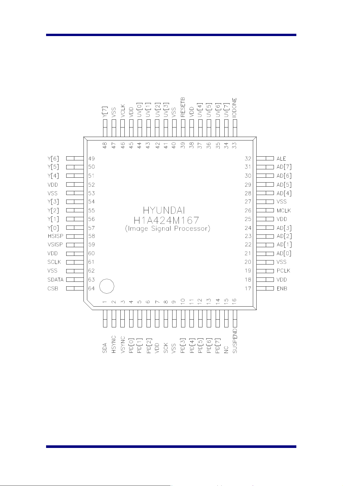
2. Pin Configuration
1999 October 11 Page 6
Page 7
Hyundai Electronics Industries Co., Ltd. H1A424M167
3. Pin Definition
Pin Number Pin Name Type Description
1 SDA B Serial Data for CMOS Image Sensor Control
2 HSYNC I Horizontal SYNC Signal from CMOS Image
Sensor
3 VSYNC I Vertical SYNC Signal from CMOS Image
Sensor
4 PD[0] I Raw Pixel Data from Image Sensor Chip
5 PD[1] I Raw Pixel Data from Image Sensor Chip
6 PD[2] I Raw Pixel Data from Image Sensor Chip
7 VDD P Power Pin, 3.3V
8 SCK O Serial Clock for CMOS Image Sensor Control
9 VSS G Ground Pin
10 PD[3] I Raw Pixel Data from Image Sensor Chip
11 PD[4] I Raw Pixel Data from Image Sensor Chip
12 PD[5] I Raw Pixel Data from Image Sensor Chip
13 PD[6] I Raw Pixel Data from Image Sensor Chip
14 PD[7] I Raw Pixel Data from Image Sensor Chip
15 NC - No Connection
16 SUSPEND I Suspend Mode Support Pin, Active high
17 ENB O CMOS Image Sensor Enable
18 VDD P Power Pin, 3.3V
19 PCLK O Pixel Clock for CMOS Sensor ( MCLK / 3 )
20 VSS G Ground Pin
21 AD[0] B Address/Data Bus for MCU interface
22 AD[1] B Address/Data Bus for MCU interface
23 AD[2] B Address/Data Bus for MCU interface
24 AD[3] B Address/Data Bus for MCU interface
25 VDD P Power Pin, 3.3V
26 MCLK I Master Clock Input
27 VSS G Ground Pin
28 AD[4] B Address/Data Bus for MCU interface
29 AD[5] B Address/Data Bus for MCU interface
30 AD[6] B Address/Data Bus for MCU interface
1999 October 11 Page 7
Page 8
Hyundai Electronics Industries Co., Ltd. H1A424M167
31 AD[7] B Address/Data Bus for MCU interface
32 ALE I Address Latch Enable
33 IODONE O CIS/ISP Read/Write Done
34 UV[7] O Video Data Output for CrCb
35 UV[6] O Video Data Output for CrCb
36 UV[5] O Video Data Output for CrCb
37 UV[4] O Video Data Output for CrCb
38 VDD P Power Pin, 3.3V
39 RESETB I ISP Reset, Active Low
40 VSS G Ground Pin
41 UV[3] O Video Data Output for CrCb
42 UV[2] O Video Data Output for CrCb
43 UV[1] O Video Data Output for CrCb
44 UV[0] O Video Data Output for CrCb
45 VDD P Power Pin, 3.3V
46 VCLK O Pixel Clock for Video Output
47 VSS G Ground Pin
48 Y[7] O Video Data Output for Y
49 Y[6] O Video Data Output for Y
50 Y[5] O Video Data Output for Y
51 Y[4] O Video Data Output for Y
52 VDD P Power Pin, 3.3V
53 VSS G Ground Pin
54 Y[3] O Video Data Output for Y
55 Y[2] O Video Data Output for Y
56 Y[1] O Video Data Output for Y
57 Y[0] O Video Data Output for Y
58 HSISP O Horizontal SYNC Signal for Video Data Output
59 VSISP O Vertical SYNC Signal for Video Data Output
60 VDD P Power Pin, 3.3V
61 SCLK/IOR I Serial Bus Clock for programming ISP, Can be
used as IOR when MCU interface configuration
62 VSS G Ground Pin
63 SDATA/IOW B Serial Bus Data for programming ISP, Can be
used as IOW when MCU interface configuration
1999 October 11 Page 8
Page 9

Hyundai Electronics Industries Co., Ltd. H1A424M167
64 CSB/MODE I ISP chip select when MCU interface
configuration
During reset time, this pin operates as
interface mode
1999 October 11 Page 9
Page 10
Hyundai Electronics Industries Co., Ltd. H1A424M167
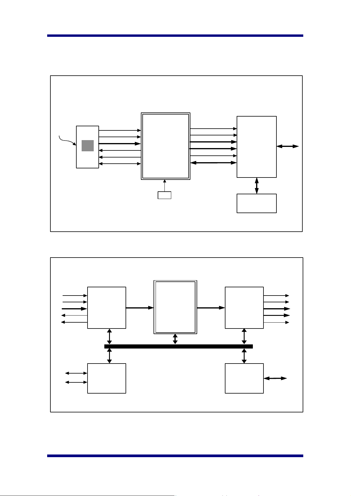
Controller
Video Buffer
4. System Diagram
HYUNDAI
CMOS Image Sensor
Image
HSYNC
VSYNC
PD[7:0]
PCLK
ENB
Serial Interface
H1A424M167
HYUNDAI ISP
MCLK
HSISP
VSISP
Y[7:0]
UV[7:0]
VCLK
Serial Interface
or Parallel Interface
USB
USB
5. Block Diagram
HSYNC
VSYNC
PD[7:0]
PCLK
ENB
SDA
SCK
Video
Input
Interface
Serial
Interface
Master
(to CIS)
Video
Processing
Engine
DRAM
Video
Ouput
Interface
MCU
Interface
( Serial or
Parallel )
HSISP
VSISP
Y[7:0]
UV[7:0]
VCLK
Serial Interface or
Parallel Interface
1999 October 11 Page 10
Page 11
Hyundai Electronics Industries Co., Ltd. H1A424M167
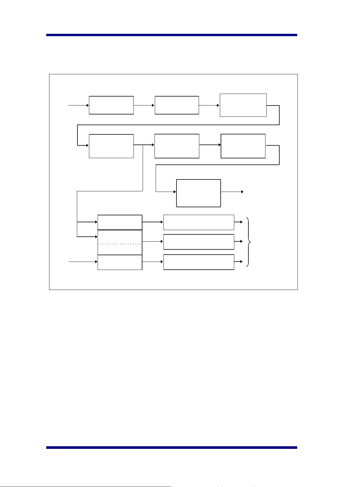
6. Video Processing Engine Block Diagram
Bayer format
RGB Stream
Interpolation
to 24bit RGB
Color
Correction
Gamma
Correction
Reset Level
Offset Data
YCrCb
Y
Color Space
Conversion
Auto White
Balance
Auto Exposure
Anti Flicker
Auto Reset
Level
Histogram
Equalization
Format
conversion
RGB Analog gain control
Integration Time Setting
Reset Level Setting
Edge
Enhnacement
YCrCb
Output Stream
To CIS
1999 October 11 Page 11
Page 12
Hyundai Electronics Industries Co., Ltd. H1A424M167
7. Functional Description
7.1. Host Interface
Hyundai ISP chip supports two kinds of host interface, serial and 8bit parallel, to
program ISP registers or to read ISP registers. And the host interface is also used to
write or to read CMOS Image Sensor(CIS) registers through ISP.
7.1.1. Serial Interface
The serial interface of Image Signal Processor[ISP] is implemented by the following
pins.
SCLK: Serial Clock SDATA: Serial Data
7.1.1.1. WRITE OPERATION
Write transaction between the ISP and a host is the similar as the well-known I2C serial
interface except that only one byte transfer at each transaction is allowed. The
transaction consists of START CONDITION, DEVICE ADDR + R/W[0], SUB ADDR,
WRITE DATA, and STOP CONDITION states. The single write access sequence is as
follows.
S DEVICE ADDR A1 SUB ADDR A2 WRITE DATA A3 P
[ S ] Operation start condition
[ DEVICE ADDR ] ISP 40h(010_0000 + 0), CIS 22h(001_0001 + 0)
ð device address + R/W bit
[ A1 ] Acknowledge from ISP
[ SUB ADDR ] ISP Sub address space 80h ~ FFh
CIS Sub address space 00h ~ 7Fh
[ A2 ] Acknowledge from ISP
[ WRITE DATA ] Register Value from host
[ A3 ] Acknowledge from ISP
[ P ] Operation stop condition
7.1.1.2. READ OPERATION
Read transaction between the ISP and a host proceeds as the following sequence.
START CONDITION ð DEVICE ADDR + R/W[0] ð SUB ADDR ð START
CONDITION ð DEVICE ADDR + R/W[1] ð READ DATA ð STOP CONDITION
The ISP register access throughput is one byte at each read transaction. But the
1999 October 11 Page 12
Page 13
Hyundai Electronics Industries Co., Ltd. H1A424M167
CMOS Image Sensor register access through the ISP chip needs two sequential read
operations to compensate the read access delay from CMOS Image Sensor to ISP.
The second read data for the CMOS image sensor register should be recognized as
the right value of the accessed register. But when the ISP auto functions are enabled,
there will be a variable delay for the right data transfer from the CMOS image sensor to
the ISP at the first read access, so the second read access may not get acknowledge
from the ISP until the first read access is completely processed in the ISP. To take care
of the said situation, a system host should repeat the second read access until it get
acknowledge from the ISP or there should be sufficient delay between two accesses.
To summarize, the ISP general register read access is always completed by only one
read transaction, and the CMOS image sensor register access needs two fully
acknowledged read transactions and the last read data is the right value for the
accessed register.
The single read access sequence is as follows.
S1 DADDR 1 A1 SADDR A2 S2 DADDR 2 A3 READ DATA A4 P
[ S1 ] Start condition
[ DADDR 1 ] Device Address ISP 40h(010_0000 + 0),
CIS 22h(001_0001 + 0)
ð device address + R/W bit
[ A1 ] Acknowledge from ISP
[ SADDR ] ISP Sub address space 80h ~ FFh
CIS Sub address space 00h ~ 7Fh
[ A2 ] Acknowledge from ISP
[ S2 ] Start condition
[ DADDR 2 ] Device Address ISP 41h(010_0000 + 1),
CIS 23h(001_0001 + 1)
ð device address + R/W bit
[ A3 ] Acknowledge from ISP
[ READ DATA ] Register Value from ISP
[ A4 ] Acknowledge from HOST
[ P ] Stop condition
* Note ( Importance ! )
ISP General Register Read : 1 Read Operation needed.
CIS Register Read : 2 Read Operation needed, valid data at second read operation.
ISP recognize CIS read command at first read.
1999 October 11 Page 13
Page 14
Hyundai Electronics Industries Co., Ltd. H1A424M167
7.1.1.3. Data Transfer Timing on the serial Interface
SDA
SCL
S
START
CONDITION
1-7
1-7
ADDRESS
ADDRESS
8 9
8 9
R/W
R/W
ACK
ACK
1-7
DATA
8 9
ACK
1-7
DATA
8 9
ACK
P
STOP
CONDITION
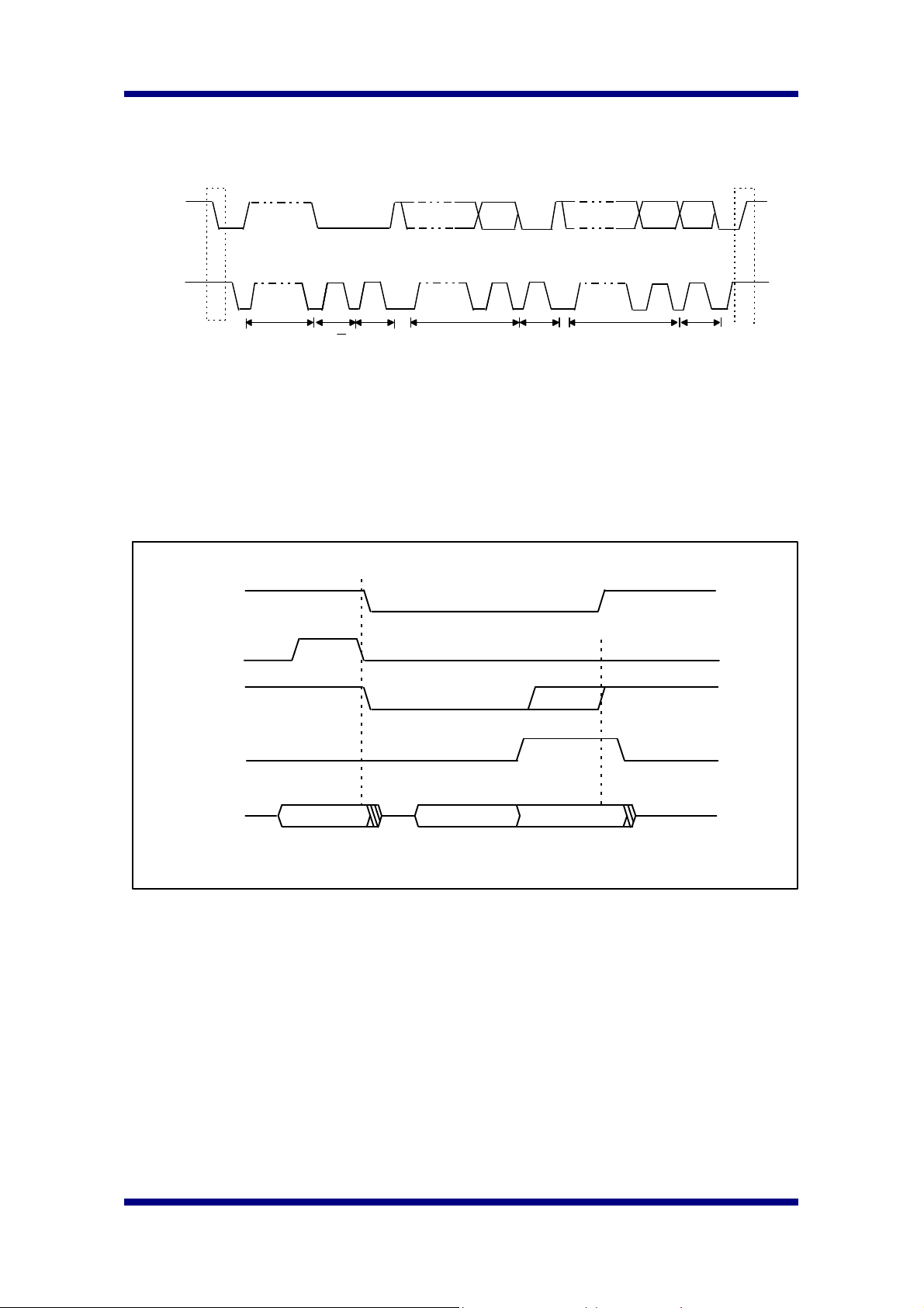
7.1.2. Host Parallel Interface
H1A424M167 ISP supports an external 8-bit microcontroller interface to access
H1A424M167 internal registers.
Basically, the data transfer operations(8bits) are multiplexed on the address bus.
CSB
ALE
IOR
Stretched
IODone
AD[7:0]
A[7:0] D[7:0]
Valid D[7:0]
Host Parallel Read Operation
A Parallel read operation always needs only 1 read cycle different from the serial read
operation. But the host must watch ‘ IODone’ signal for a proper read operation. IODone
signal indicates the completion of read/write operation. So the host must hold the IOR,
CSB signals until IODone signal is active, to read the valid data on AD[7:0] lines. At the
final stage, the host ends the bus cycle(CSB, IOR) then IODone signal become
inactive.
1999 October 11 Page 14
Page 15
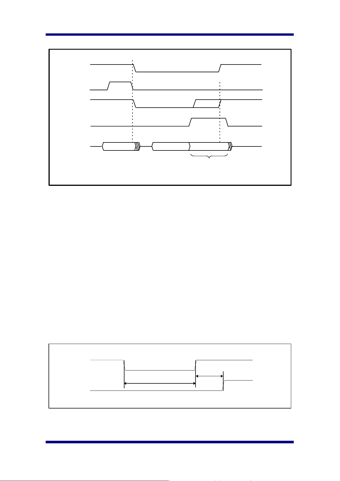
Hyundai Electronics Industries Co., Ltd. H1A424M167
IOW
CSB
Host Parallel Write Operation
ALE
Stretched
IODone
AD[7:0]
A[7:0] D[7:0]
Stretched
Active write operation
Similar to parallel read operation, parallel write operation needs only 1 operation cycle.
The host must watch ‘ IODone’ signal for a proper write operation. IODone signal
indicates the completion of read/write operation. So the host must hold the IOW, CSB,
Write Data[7:0] signals until IODone signal become active. When IODone signal
become active, ISP accept the write data internally. At the final stage, the host ends the
bus cycle(CSB, IOW, Write Data[7:0]) and IODone signal become inactive.
ISP holds IODone active until read/write operation is completed. CIS register read/write
operation needs more time than ISP register read/write operation. So IODone active
signal for CIS register read/write operation is much longer than that of ISP register
read/write operation.
7.1.3. Serial or Parallel Interface selection
The selection between serial interface and parallel interface is made at hardware reset
time. If CSB/MODE pin, pin number 64, is pulled down during reset, Serial Interface is
configured, and otherwise parallel interface is selected.
For example, Serial Interface selection timing is as below.
RESETB
CSB/MODE
1999 October 11 Page 15
More than 64 MCLK
Serial Interface Selection
Page 16

Hyundai Electronics Industries Co., Ltd. H1A424M167
7.2. Clock(MCLK, PCLK, VCLK) Timing Diagram
This chart shows the timing diagram in the YCbCr 4:2:2, 16bit video mode.
MCLK
PCLK
VCLK
Y[7:0]
UV[7:0]
VCLK
Y[7:0]
UV[7:0]
Y0 Y1 Y2 Y3
U0 V0 U2
OP_MODE (VGA)
Y0 Y1
U0 V0 U2
OP_MODE (SIF,CIF,QSIF,QCIF)
V2
Y4 Y5
U4 V4
Y2
* Note : HV7131B(VGA) CMOS Sensor is used for this timing diagram.
7.3. Video Output Interface
The H1A424M167 outputs video data in YUV 4:2:2 format through the 16-bit (Y[7:0]
and UV[7:0]) data bus. Video data is changed at the rising edge of the VCLK signal. UV
order can be selected by programming OUT_FORM register. VCLK frequency is same
to PCLK frequency in VGA mode when the 16-bit video mode is enabled. VCLK
frequency is a half of PCLK frequency in SIF,CIF,QSIF,QCIF modes when the 16-bit
video mode is enabled. (See OP_MODE register description.)
Some video codec needs several HSYNC pulses within active VSYNC. So, The
H1A424M167 can modify input VSYNC width by programming HSYNC_COUNT
register for VSISP pulse to contain several HSYNC pulses.
All YUV 16bit ports are active for every HSISP lines in YUV 4:2:2, 16bit video mode.
All YUV 16bit ports are active for even HSISP lines, and only Y 8bit ports are active for
1999 October 11 Page 16
Page 17

Hyundai Electronics Industries Co., Ltd. H1A424M167
odd HSYNC lines in YUV 4:2:0, 16bit video mode.
The following chart shows the video output data format in the 4:2:2, 4:2:0,16bit video
mode.
VSISP
HSISP
Y[0..8]
UV[0..8]
VSISP
HSISP
Y[0..8]
UV[0..8]
Y0 Y1 Y2 Y3 Y0 Y1 Y2 Y3 Y0 Y1 Y2
U0 V0 U2 V2 U0 V0 U2 V2 U0 V0 U2 V2 U0 V0 U2 V2
Y3
Y0 Y1 Y2
YCbCr 4:2:2, 16bit format, Cb first
Y0 Y1 Y2 Y3 Y0 Y1 Y2 Y3
Don’ t Care
U0 V0 U2 V2 U0 V0 U2 V2
Y0 Y1 Y2
Don’ t Care
Y3
Y0 Y1 Y2
YCbCr 4:2:0, 16bit format, Cb first
Y3
Y3
VICLK
Y[7:0]
UV[7:0]
Y0 Y1 Y2 Y3
U0 V0 U2
V2
Y4 Y5
U4 V4
OUT_FORM (Cr first)
Y[7:0]
UV[7:0]
Y0 Y1 Y2 Y3
V0 U0 V2 U2
Y4 Y5
V4 U4
OUT_FORM (Cb first)
1999 October 11 Page 17
Page 18

Hyundai Electronics Industries Co., Ltd. H1A424M167
7.4. Relations between input video timing and output video timing
The H1A424M167 have five modes of video output timing - VGA(640X480),
CIF(352X288), SIF(320X240), QCIF(176X144), QSIF(160X120) - , when the CMOS
Image sensor operates in mode of VGA(640X480). The first pixel color of a frame
should be “RED” in order to get correct color interpolated image.
The following timing diagrams show relations on each mode.
7.4.1. VGA
VSYNC
HSYNC
SENSOR
DATA
VSISP
HSISP
YUV
7.4.2. CIF
VSYNC
HSYNC
SENSOR
DATA
VSISP
Output Delay
not considered.
Output Delay
not considered.
CIS Output Timing
ISP Output Timing
CIS Output Timing
HSISP
YUV
ISP Output Timing
1999 October 11 Page 18
Page 19

Hyundai Electronics Industries Co., Ltd. H1A424M167
7.4.3. SIF
VSYNC
HSYNC
SENSOR
DATA
VSISP
HSISP
YUV
7.4.4. QCIF
VSYNC
HSYNC
SENSOR
DATA
Output Delay
not considered.
CIS Output Timing
ISP Output Timing
Output Delay
not considered.
CIS Output Timing
VSISP
HSISP
YUV
ISP Output Timing
1999 October 11 Page 19
Page 20

Hyundai Electronics Industries Co., Ltd. H1A424M167
7.4.5. QSIF
VSYNC
HSYNC
SENSOR
DATA
VSISP
HSISP
YUV
Output Delay
not considered.
CIS Output Timing
ISP Output Timing
1999 October 11 Page 20
Page 21

Hyundai Electronics Industries Co., Ltd. H1A424M167
8. Register Description
8.1. Registers Mnemonic Table
l BASE Registers Table
Register Name Mnemonic Address Default
Operating Mode Register OP_MODE 80h 02h
Base Function Enable Register BASE_ENB 81h 01h
Scale Width Control Upper Register SCALE_UPPER 82h 01h
Scale Width Control Lower Register SCALE_LOWER 83h 40h
CMA11 Register CMA11 8Ah 5Ah
CMA12 Register CMA12 8Bh F3h
CMA13 Register CMA13 8Ch F3h
CMA21 Register CMA21 8Dh F3h
CMA22 Register CMA22 8Eh 5Ah
CMA23 Register CMA23 8Fh F3h
CMA31 Register CMA31 90h F3h
CMA32 Register CMA32 91h F3h
CMA33 Register CMA33 92h 5Ah
OFSR Register OFSR 93h 00h
OFSG Register OFSG 94h 00h
OFSB Register OFSB 95h 00h
l AUTO Registers Table
Register Name Mnemonic Address Default
Auto Function Enable Register AUTO_ENB A0h 00h
AWB/AE Window Horizontal Start
Position Ha
Horizontal Side Segment Width Hb WIN_H_SIDE A2h 96h
Horizontal Center Segment Width Hc WIN_H_CENTER A3h FAh
AWB/AE Window Vertical Start
WIN_H_START A1h 2Dh
WIN_V_START A4h 0Ah
Position Va
Vertical Side Segment Height Vb WIN_V_SIDE A5h 50h
Vertical Center Segment Height Vc WIN_V_CENTER A6h 0Ah
Analog Gain-Top Limit Register GAIN_TOP A7h 3Fh
Analog Gain-Bottom Limit Register GAIN_BOTTOM A8h 14h
1999 October 11 Page 21
Page 22

Hyundai Electronics Industries Co., Ltd. H1A424M167
AWB Function Control Register AWB_CONTROL A9h 76h
AWB Lock Control Register AWB_LOCK AAh B5h
AE Function Control Register AE_CONTROL ABh 55h
AE Lock Control Register AE_LOCK ACh B5h
Y-target Value Register Y_TARGET ADh 80h
Reset Level Control Register RESET_LEVEL AEh 20h
Exposure Time Limitation Value
EXP_LMT_UPPER B0h 14h
Upper Byte
Exposure Time Limitation Value
EXP_LMT_MIDDLE B1h 58h
Middle Byte
Exposure Time Limitation Value
EXP_LMT_LOWER B2h 55h
Lower Byte
AWB Cr-target Value Register AWB_CR_TARGET B3h 80h
AWB Cb-target Value Register AWB_CB_TARGET B4h 80h
Anti Flicker Unit Time Upper Byte AF_UT_UPPER B5h 01h
Anti Flicker Unit Time Middle Byte AF_UT_MIDDLE B6h B2h
Anti Flicker Unit Time Lower Byte AF_UT_LOWER B7h 07h
Lock Status Flags Register(Read Only) STATUS_FLAGS B8h XXh
l OUT Registers Table
Register Name Mnemonic Address Default
Edge Control Register EDGE_CONTROL C0h 0Dh
Output Format Control Register OUT_FORM C1h 08h
HSYNC Counter Register HSYNC_COUNT C2h 06h
Manual Histogram Mode Control Register
Fixed Contrast Stretching Factor Register
HISTO_MODE C3h 00h
FIXED_FACTOR C4h 00h
Gamma Start 0 Register GMA_START0 E0h 20h
Gamma Start 1 Register GMA_START1 E1h 2Dh
Gamma Start 2 Register GMA_START2 E2h 37h
Gamma Start 3 Register GMA_START3 E3h 47h
Gamma Start 4 Register GMA_START4 E4h 5Fh
Gamma Start 5 Register GMA_START5 E5h 72h
Gamma Start 6 Register GMA_START6 E6h 83h
Gamma Start 7 Register GMA_START7 E7h B6h
Gamma Start 8 Register GMA_START8 E8h DEh
1999 October 11 Page 22
Page 23

Hyundai Electronics Industries Co., Ltd. H1A424M167
Gamma Slope 0 Register GMA_SLOPE0 E9h 19h
Gamma Slope 1 Register GMA_SLOPE1 EAh 28h
Gamma Slope 2 Register GMA_SLOPE2 EBh 1Fh
Gamma Slope 3 Register GMA_SLOPE3 ECh 18h
Gamma Slope 4 Register GMA_SLOPE4 EDh 13h
Gamma Slope 5 Register GMA_SLOPE5 EEh 10h
Gamma Slope 6 Register GMA_SLOPE6 EFh 0Ch
Gamma Slope 7 Register GMA_SLOPE7 F0h 09h
Gamma Slope 8 Register GMA_SLOPE8 F1h 08h
1999 October 11 Page 23
Page 24

Hyundai Electronics Industries Co., Ltd. H1A424M167
8.2. BASE Register Map
( MCU Address Space 80h~95h )
8.2.1. Normal Register[80h~83h]
Operating Mode Register[80h] [02h]
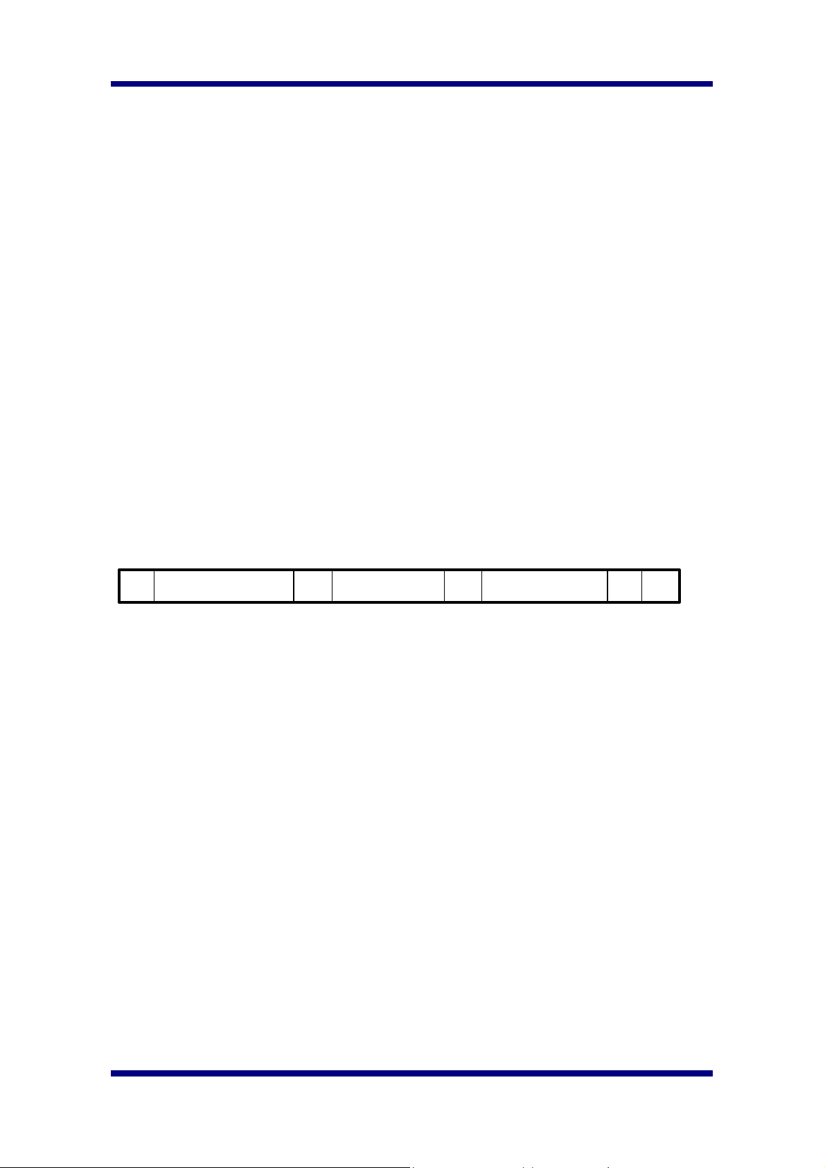
[7] [6] [5] [4] [2] [1] [0]
[ 7..6 ] Sensor PCLK divider [R/W]
0 : MCLK/3, 1: MCLK/6, 2: MCLK/12, 3: MCLK/24
* Note : Normally, use MCLK/3 with VGA(HV7131X), CIF(HV7121X) CIS
[ 5..4 ] ISP Clock divider [R/W]
0 : MCLK/3, 1: MCLK/6, 2: MCLK/12, 3: MCLK/24
* Note : Normally, use MCLK/3 with VGA(HV7131X) CIS, MCLK/6 with CIF(HV7121X)
CIS
[ 2..0 ] Operating Mode Set [R/W]
1 0 0 : VGA ( 1 to 1 Mode )
0 1 1 : C I F ( Subsample Mode )
0 1 0 : S I F ( Subsample Mode )
0 0 1 : QCIF ( Subsample Mode )
0 0 0 : QSIF ( Subsample Mode )
These bits specifies which one of color interpolation methods is used,
VGA : color interpolation using 3x3 spatial kernel
CIF/SIF : color interpolation using 3/4 subsampling using 2x2 kernel
QCIF/QSIF : color interpolation using 3/16 subsampling using 4x4 kernel
and also specifies which one of input image size scalings is used.
VGA : 1/1 scaling
CIF/SIF : 1/4 scaling
QCIF/QSIF : 1/16 scaling
a) Subsampling mode definitions
3/4 subsampling : 2x2 Bayer Data for four sensor pixels.
ð R/G/B Data for a output pixel in CIF/SIF mode.
Subsampling window moves by 2 pixels in horizontal
and vertical directions.
3/16 subsampling: 4x4 Bayer Data for sixteen sensor pixels.
ð R/G/B Data for a output pixel in QCIF/QSIF mode.
Subsampling window moves by 4 pixels in horizontal
and vertical directions.
b) In VGA(1 to 1 Mode) mode operation, ISP needs the input image with 642 X
482 size for horizontal and vertical interpolation. In CIF,SIF,QCIF,QSIF
(Subsample Mode) mode operation, ISP needs the input image with 640 X
482 for vertical interpolation. The reason that vertical height is two lines plus
480 is that internal ISP logic requires two lines timing margin to support
CIF/QCIF/X-flip functions. For CIF mode, horizontal blank period of a sensor
must be larger than 64 pixel clock.
1999 October 11 Page 24
Page 25

Hyundai Electronics Industries Co., Ltd. H1A424M167
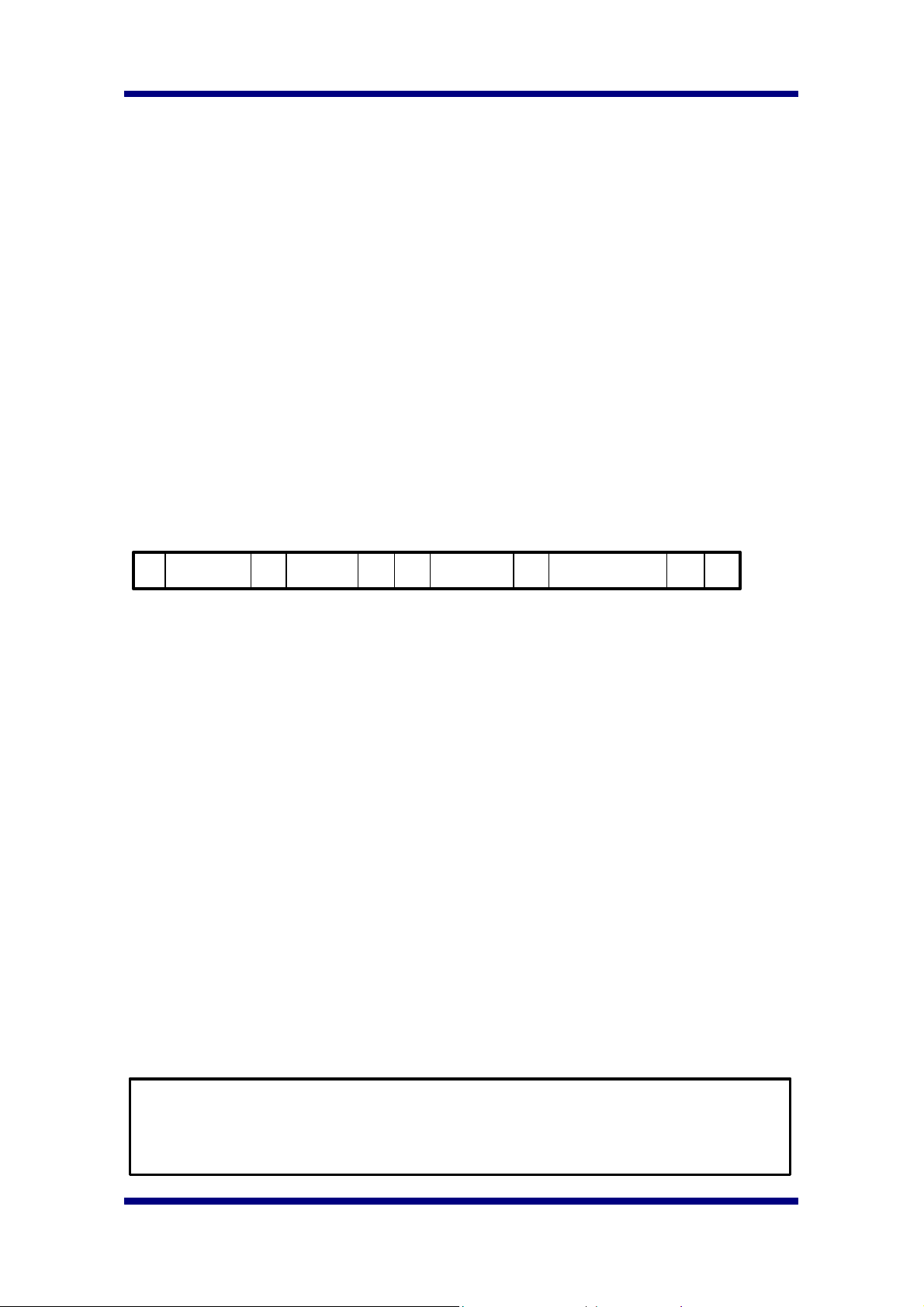
Base Function Enable Register[81h] [01h]
[5] [4] [3] [2] [1] [0]
[ 5 ] RB Interpolation Mode Set [R/W]
Two R/B color interpolation methods are supported when R or B color
component is interpolated from neighbor pixels’ s information for full RGB color
in VGA mode:
a) average mode that interpolates missing R or B by just averaging neighbor
R or B pixels,
b) chromacity mode that interpolates missing R or B from utilizing neighbor
chromacitis values, (R-G) or (B-G).
This bit specifies which one of the color interpolation methods is used
1 : Average, 0 : Chromacity
[ 4 ] G Interpolation Mode Set [R/W]
Two G color interpolation methods are supported when G color component is
interpolated from neighbor G pixels's information for full RGB color in VGA
mode:
a) median mode that interpolates missing G by averaging median neighbor
G values excluding maximum/minimum neighbor G values.
b) average mode that interpolates missing G by averaging all neighbor G
values.
This bit specifies which one of G color interpolation methods is used
1 : Median, 0 : Average
[ 3 ] X-Flip Function Enable [R/W]
The function enables the horizontal flip(left-right changed) of input image data.
In oder to get the flipped standard image size(640x480) with VGA
interpolation mode selected, input image data input size should be 642x483
that height size is one more line increased, to account for Bayer input data to
be flipped before any processing proceeds.
For other flipped image size format outputs(CIF/SIF/QCIF/QSIG), the input
image size is the same as that for unflipped image data out, 640x482.
1: X-Flip ON, 0 : X-Flip OFF
[ 2 ] Gamma Function Enable [R/W]
Piecewise linear gamma approximation method is implemented. Precise piece
linear segments are supported and user-programmable.
For more details, refer to gamma register description section.
1 : Gamma ON, 0 : Gamma OFF
[ 1 ] Color Matrix Function Enable [R/W]
This function compensates color spread effect of color filters and sensing
circuits to get the optimal pure color reproduction. color matrix coefficients are
programmable from -127/64 to 127/64. Offset compensation registers are also
supported.
1 : Color Matrix ON, 0 : Color Matrix OFF
1999 October 11 Page 25
Page 26

Hyundai Electronics Industries Co., Ltd. H1A424M167
[ 0 ] Color Interpolation Function Enable [R/W]
This bit specifies whether color interpolation is processed or not. Color
interpolation methods are defined by OP_MODE register. Most importantly, in
order to have a correct color interpolation, the first input pixel data type should
be R pixel data.
1 : Interpolation ON, 0 : Interpolation OFF
* Note : The start pixel of every input frame must be R for proper interpolation.
Scale Width Control Upper Register[82h] [01h]
[0]
[ 0 ] Scale Width Control Upper Value [R/W]
Scale Width Control Lower Register[83h] [40h]
[7] [6] [5] [4] [3] [2] [1] [0]
[ 7..0 ] Scale Width Control Lower Value [R/W]
* Note : The scale width control register is only related to operating mode
CIF/SIF/QCIF/QSIF, and controls how many column data in each line are output.
Default value is 140h(340d), the half of standard VGA width size.
8.2.2. Color Matrix Coefficients Value[8Ah ~ 95h]
These registers are used in color matrix function in order to compensates color spread
effect of color filters and sensing circuits to get the optimal pure color reproduction.
Color matrix coefficients are programmable from -127/64 to 127/64. Programming
register value for intended color matrix coefficients should be resolved by the following
sequence.
For positive values,
CMAxx = Integer(RealCoefficientValue x 64);
For negative values,
CMAxx = TwosComplement(Integer(RealCoefficientValue x 64));
RealCoefficientValue values from -127/64 to 127/64 can be programmed.
Offset compensation registers are also supported.
1999 October 11 Page 26
Page 27

Hyundai Electronics Industries Co., Ltd. H1A424M167
l Fundamental color matrix equation
CMA11 CMA12 CMA13
CMA21 CMA22 CMA23
CMA31 CMA32 CMA33
R
G
+
B
OFSR
OFSG
OFSB
CMA11 Register[8Ah] [5Ah]
[7] [6] [5] [4] [3] [2] [1] [0]
[ 7..0 ] CMA11 Value X 64 2’ s Complement [R/W]
CMA12 Register[8Bh] [F3h]
[7] [6] [5] [4] [3] [2] [1] [0]
[ 7..0 ] CMA12 Value X 64 2’ s Complement [R/W]
CMA13 Register[8Ch] [F3h]
[7] [6] [5] [4] [3] [2] [1] [0]
[ 7..0 ] CMA13 Value X 64 2’ s Complement [R/W]
CMA21 Register[8Dh] [F3h]
[7] [6] [5] [4] [3] [2] [1] [0]
[ 7..0 ] CMA21 Value X 64 2’ s Complement [R/W]
CMA22 Register[8Eh] [5Ah]
[7] [6] [5] [4] [3] [2] [1] [0]
[ 7..0 ] CMA22 Value X 64 2’ s Complement [R/W]
CMA23 Register[8Fh] [F3h]
[7] [6] [5] [4] [3] [2] [1] [0]
[ 7..0 ] CMA23 Value X 64 2’ s Complement [R/W]
CMA31 Register[90h] [F3h]
[7] [6] [5] [4] [3] [2] [1] [0]
[ 7..0 ] CMA31 Value X 64 2’ s Complement [R/W]
CMA32 Register[91h] [F3h]
[7] [6] [5] [4] [3] [2] [1] [0]
[ 7..0 ] CMA32 Value X 64 2’ s Complement [R/W]
1999 October 11 Page 27
Page 28

Hyundai Electronics Industries Co., Ltd. H1A424M167
CMA33 Register[92h] [5Ah]
[7] [6] [5] [4] [3] [2] [1] [0]
[ 7..0 ] CMA33 Value X 64 2’ s Complement [R/W]
OFSR Register[93h] [00h]
[7] [6] [5] [4] [3] [2] [1] [0]
[ 7..0 ] Color Matrix Red Offset Value -127 ~ +128 2’ s complement [R/W]
OFSG Register[94h] [00h]
[7] [6] [5] [4] [3] [2] [1] [0]
[ 7..0 ] Color Matrix Green Offset Value -127 ~ +128 2’ s complement [R/W]
OFSB Register[95h] [00h]
[7] [6] [5] [4] [3] [2] [1] [0]
[ 7..0 ] Color Matrix Blue Offset Value -127 ~ +128 2’ s complement [R/W]
* Note : The values of CMA11~CMA33 are allowed between -2 and 2
1999 October 11 Page 28
Page 29

Hyundai Electronics Industries Co., Ltd. H1A424M167
8.3. AUTO Register Map
( MCU Address Space A0h ~ B4h )
8.3.1. Function Enable Register[A0h]
Auto Function Enable Register[A0h] [00h]
[7] [6] [5] [4] [3] [1] [0]
[ 7 ] Image Sensor ENB Control [R/W]
1 : ENB enable, 0 : ENB disable
[ 6 ] AE Mode Control 1 [R/W]
Used with AE mode control 0 at bit 0
[ 5 ] Auto Histogram Equalization Enable [R/W]
Automatically enables the histogram equalization function when larger
exposure time than exposure time limit value defined at the registers B0 ~ B2
is needed to achieve Y target brightness. This bit is not valid when manual
histogram equalization defined at register C3h is enabled.
1 : Auto Histogram Equalization ON
0 : Auto Histogram Equalization OFF
[ 4 ] Automatic Reset Level Control [R/W]
Automatically controls the Reset Level of CMOS Image Sensor. Low
Reference Count Register and High Reference Count Register (Hyundai
CMOS Image Sensor Registers, Addressed 57h 58h 59h 5ah) denote the
current sampling condition. when the ARC function enable, ARC logic reads
these register values and compares with the threshold value within the Reset
Level Control Register(ISP Register Addressed AEh). If the low reference
count or high reference count is larger than the value of Reset Level Control
Register, ARC Logic considers Reset Level is not suitable for fine sampling,
and update the appropriate Reset Level Value in the Reset Level
Register(30h) of HYUNDAI CMOS Image Sensor.
1 : ARC on, 0 : ARC off
[ 3 ] Automatic G-color gain Control [R/W]
AWB Logic control only the R, B color gain of CIS. So, for getting better color
balance and using large analog gain range, G color gain must be controlled. If
this function(AGC) is enabled, AGC Logic control appropriate G-color gain
level automatically. It may be disabled, when the analog gain range(Limited by
analog gain Top, Bottom Limit Register) is too small.
1 : AGC on, 0 : AGC off
1999 October 11 Page 29
Page 30

Hyundai Electronics Industries Co., Ltd. H1A424M167
HaHbHcHbVaVbVcVbAHstartBReg(
Hb)
AHstartCReg(
Hc)
AVstartAReg(
Va)
AVstartBReg(
Vb)
AVstartCReg(
Vc)
AHstartAReg(Ha)
[ 1 ] AWB Function Control [R/W]
1 : AWB On, 0 : AWB Off
[ 0 ] AE Mode Control 0 [R/W]
Define AE mode with AE mode control 1 at bit 6
AE mode control 1 AE mode control 0 AE mode
0 0 AE disable
0 1 AE pixel mode
1 X AE anti-flicker mode
8.3.2. AWB/AE Windows Configuration Registers[A1h~A6h]
Hyundai H1A424M167 analyze the input image from the CMOS Image Sensor, base
on the 9 programmable windows for AE and AWB. The AE and AWB function use Y
and U,V values from 9 independent windows to adjust brightness and to correct color
balance.
l AWB/AE Windows Configuration
Full Frame Window
AE Window
A
Window
B
Window
A
Window
B
Window
C
Window
B
Window
A
Window
B
Window
A
Window
AWB/AE Window Horizontal Start Position Ha [A1h] [2Dh]
[7] [6] [5] [4] [3] [2] [1] [0]
[ 7..0 ] A-Windows Horizontal Size Pixel Count Value [R/W]
Horizontal Side Segment Width Hb [A2h] [96h]
[7] [6] [5] [4] [3] [2] [1] [0]
[ 7..0 ] B-Windows Horizontal Size Pixel Count Value [R/W]
1999 October 11 Page 30
Page 31

Hyundai Electronics Industries Co., Ltd. H1A424M167
Horizontal Center Segment Width Hc [A3h] [FAh]
[7] [6] [5] [4] [3] [2] [1] [0]
[ 7..0 ] C-Windows Horizontal Size Pixel Count Value [R/W]
AWE/AE Window Vertical Start Position Va [A4h] [0Ah]
[7] [6] [5] [4] [3] [2] [1] [0]
[ 7..0 ] A-Windows Vertical Size Pixel Count Value [R/W]
Vertical Side Segment Height Vb [A5h] [50h]
[7] [6] [5] [4] [3] [2] [1] [0]
[ 7..0 ] B-Windows Vertical Size Pixel Count Value [R/W]
Vertical Center Segment Height Vc [A6h] [0Ah]
[7] [6] [5] [4] [3] [2] [1] [0]
[ 7..0 ] C-Windows Vertical Size Pixel Count Value [R/W]
* Note : When the display mode is not VGA, Horizontal Configuration value (Ha, Hb,
Hc) have to be programmed as two times larger value of actual Horizontal display size.
8.3.3. Normal Register[A7h~B8h]
Analog Gain-Top Limit Register[A7h] [3Fh]
[7] [6] [5] [4] [3] [2] [1] [0]
[ 7..0 ] Analog Gain-Top Value(Analog Gain Level Boundary) [R/W]
Analog Gain-Bottom Limit Register[A8h] [14h]
[7] [6] [5] [4] [3] [2] [1] [0]
[ 7..0 ] Analog Gain-Bottom Value(Analog Gain Level Boundary) [R/W]
CMOS Image Sensor supports analog gain function to amplify the pixel analog output
of CMOS Sensor. Available programmable range is 0 - 63. If the analog gain is too
large or too small, the dynamic range of sensor pixel output is not suitable for fine
scene. These registers(A7h,A8h) define the usable analog gain range (maximum and
minimum gain) of CIS for ISP to control R,G,B gain of CMOS Image Sensor within this
range. Available programmable range is 0 - 63 and the value of analog gain-Top limit
register must be larger than the value of analog gain-Bottom Limit register.
AWB Function Control Register[A9h] [76h]
[7] [6] [5] [4] [3] [2] [1] [0]
This Register is used to define the pixels to be accumulated for AWB. Only the pixels
1999 October 11 Page 31
Page 32

Hyundai Electronics Industries Co., Ltd. H1A424M167
within the defined color and luminous range on this register will be used for AWB.
[ 7. .5 ] Cr+Cb Range Selector [R/W]
[ 4. .2 ] Cr Range Selector [R/W]
* Note : 0 to 7 are allowed for Cr+Cb range and Cr range.
Larger value means wider AWB white spot.
[ 1 ] Luminous Range selector [R/W]
1 : Reject too Dark and too Bright pixels for AWB
0 : Use all pixels for AWB
[ 0 ] AwbWin [R/W]
0 : Whole 9 AWB windows used
1 : Only center AWB window used
AWB Lock Control Register[AAh] [B5h]
[7] [6] [5] [4] [3] [2] [1] [0]
This Register is used for AWB Lock Control. The difference between Cr/Cb target and
current frame Cr/Cb mean is used for AWB lock/unlock scheme. As the difference is
smaller, we can get the good white balanced image. The difference is compared with
AWB lock range value and AWB unlock range value. If current state is out of white
balance, AWB logic change the R/B gains of CMOS Image Sensor to make the
difference less than the lock range value. If the difference is less than lock range value,
we consider white balance is achieved and no more gain control made. After getting
white balanced image we have to compare the difference with unlock range value to
check the image is out of white balance or not. If the difference is larger than the unlock
range value, AWB logic start to change R/B gains again to find new white balance
point.
[ 7 ] AWB Lock_Unlock Function Enable Bit [R/W]
0 : Lock, Unlock Function Disable. In this case AWB Unlock Range is used for
both Locking and unlocking. AWB lock range is not used.
1 : Lock, Unlock Function Enable. In this case AWB lock range and AWB
unlock range are defined separately for locking and unlocking.
[ 6..4 ] AWB Lock Range
[ 3..0 ] AWB Unlock Range
* Note : When AWB lock_unlock function is enabled, AWB unlock range have to be
larger than the lock range. As the larger value of lock/unlock range, we can get the
stable image. And as the small value of lock/unlock range, we can get the fine white
balanced image.
1999 October 11 Page 32
Page 33

Hyundai Electronics Industries Co., Ltd. H1A424M167
aba
caabbbl Windows Defined for AE
AE Function Control Register[ABh] [55h]
[7] [6] [5] [4] [3] [2] [1] [0]
[ 7..6 ] Weight Mode [R/W]
These Bits are used to select weight mode of AE Function. When block weight
mode is selected, nine AE windows have different weight. When window
weight mode is selected, nine AE windows have same weight and all the pixels
in the center window(window-c) and window-b will be used for AE but pixels in
the window-a are limited by bit 4 Wweight. When block and window mixed
mode, AE windows have different weights and pixel limit function is on too by
bit 4 Wweight. When Weightless mode is selected, all the original pixel value
in the nine AE windows will be used for AE.
00 : Bweight(Block weight) Mode only.
01 : Wweight(Window weight) Mode only.
10 : BWeight + Wweight
11 : Weightless Mode
[ 5 ] Bweight [R/W]
Two kinds of Block Weight are available when Block weight mode.
0 : Smaller center window weight ( a < b < c )
1 : Larger center window weight ( a < b << c )
[ 4 ] Wweight [R/W]
Windows Weight Selector for AE when Wweight Mode Valid.
0 : Larger Y range is used.
1 : Smaller Y range is used.
[ 3..2 ] Anti_Flicker_Control (Lock Range Selector) [R/W]
Lock range select for Anti-flicker mode. Small value means fine AE control but
unstable , large value means rough AE control but stable.
[ 1 ] Histogram Equalization Fine Control [R/W]
This bit defines the Histogram Equalization method when the Histogram
Equalization function is on(Auto Function enable Register[5] = 1).
0 : Use small contrast stretching value
[ 0 ] Exposure Time update rate control. [R/W]
This bit is used to set the exposure time update rate.
1999 October 11 Page 33
1 : Use large contrast stretching value
Page 34

Hyundai Electronics Industries Co., Ltd. H1A424M167
0 : Every 2-frame.
1 : Every 3-frame.
AE Lock Control Register[ACh] [B5h]
[7] [6] [5] [4] [3] [2] [1] [0]
This Register is used for AE Lock Control. The difference between Y target and current
frame Y mean is used for AE lock/unlock scheme. As the difference is smaller, we
can get the close brightness we want . The difference is compared with AE lock range
value and AE unlock range value. If current state is out of target brightness, AE logic
change the integration time of CIS to make the difference less than the lock range
value. If the difference is less than lock range value, we consider exposure target is
achieved and no more integration time control made. After getting target brightness we
have to compare the difference with unlock range value to check the image is out of
target brightness or not. If the difference is larger than the unlock range value, we have
to change integration time again to adjust frame brightness. This register is valid only
when AE pixel mode is enabled.
[ 7 ] AE Lock_Function Enable Bit [R/W]
0 : Lock, Unlock Function Disable . In this case, AE Unlock Range is used for
all locking and unlocking. AE lock range is not used.
1 : Lock, Unlock Function Enable. In this case, AE lock range and AE unlock
range are used for locking and unlocking each.
[ 6..4 ] AE Lock Range
[ 3..0 ] AE Unlock Range
Y-target Value Register[ADh] [80h]
[7] [6] [5] [4] [3] [2] [1] [0]
[ 7..0 ] AE Target Luminous Value Register. [R/W]
Reset Level Control Register[AEh] [20h]
[7] [6] [5] [4] [3] [2] [1] [0]
[ 7..0 ] Threshold Pixel Count Value of the Invalid Reference Value. [R/W]
This Register is used to set the maximum Invalid Pixel Count, produced from CIS
sampling(data Read). So, as the small value of this Register, we can get the fine scene.
This register valid only when ARC Function(A0h[4]) is enabled.
Exposure Time Limitation Value Upper Byte[B0h] [14h]
[7] [6] [5] [4] [3] [2] [1] [0]
1999 October 11 Page 34
Page 35

Hyundai Electronics Industries Co., Ltd. H1A424M167
Exposure Time Limitation Value Middle Byte[B1h] [58h]
[7] [6] [5] [4] [3] [2] [1] [0]
Exposure Time Limitation Value Lower Byte[B2h] [55h]
[7] [6] [5] [4] [3] [2] [1] [0]
These three Exposure Time Limitation Value Registers(24Bits) are used to set the
minimum Frame-Rate. It defines maximum exposure time that can be programmed to
CIS integration time registers. And, It must be programmed as multiple of Anti Flicker
Unit Time Register(24Bits) when AE anti_Flicker mode is enabled.
AWB Cr-target Value Register[B3h] [80h]
[7] [6] [5] [4] [3] [2] [1] [0]
AWB Cb-target Value Register[B4h] [80h]
[7] [6] [5] [4] [3] [2] [1] [0]
These Cr, Cb-target Registers are used for controlling Frame Color. AWB logic use
these values for a white balance matching. To make a frame reddish, Increase the Cr
target register value over 80h or decrease the Cb target register value under 80h.
Anti Flicker Unit Time Upper Byte[B5h] [01h]
[7] [6] [5] [4] [3] [2] [1] [0]
Anti Flicker Unit Time Middle Byte[B6h] [B2h]
[7] [6] [5] [4] [3] [2] [1] [0]
Anti Flicker Unit Time Lower Byte[B7h] [07h]
[7] [6] [5] [4] [3] [2] [1] [0]
Anti Flicker Unit Time Registers(24Bits) should be used to define the time step of
changing integration time register. AE Anti-Flicker mode is used to remove horizontal
banding noise under fluorescent lamp. When AE anti-flicker mode is enabled, the
integration registers of a CIS are programmed as multiple of this unit time. These
registers are valid only when AE anti-flicker mode is enabled. When AE pixel mode is
enabled, Anti flicker Unit time Registers(24Bits) are used to set exposure time bottom
limitation.
1999 October 11 Page 35
Page 36

Hyundai Electronics Industries Co., Ltd. H1A424M167
Lock status Flags Register[B8h] [R-O]
[2] [1] [0]
User can read the current AE/AWB status using this register.
This register can be used to choose a fine image for digital still camera application.
[ 2 ] Automatic Stretching Status Flag [Read Only]
0 : Automatic Stretching is Disable.
1 : Automatic Stretching is Enable.
[ 1 ] AWB Lock Status Flag [Read Only]
0 : Current AWB status is Unlock.
1 : Current AWB status is Lock.
[ 0 ] AE Lock Status Flag [Read Only]
0 : Current AE status is Unlock.
1 : Current AE status is Lock.
1999 October 11 Page 36
Page 37

Hyundai Electronics Industries Co., Ltd. H1A424M167
8.4. OUT Register Map
( MCU Address Space C0h ~ F1h )
8.4.1. Normal Register[C0h~C2h]
Edge Control Register[C0h] [0Dh]
[3] [2] [1]
[ 3 ] 1 : Edge Function Enable, 0 : Edge Function Disable [R/W]
[ 2 ] 1 : Use Edge Transfer Function, 0 : Bypass Edge Transfer Function[R/W]
[ 1 ] Edge detection filter select [R/W]
1: -1/2, 0 , 1, 0, -1/2
0: 0, -1/2, 1, 0, -1/2
Output Format Control Register[C1h] [08h]
[5] [4] [3] [2] [1] [0]
[ 5 ] 0 : Use CCIR-601 Color Space Conversion equation [R/W]
1 : Use JFIF Color Space Conversion equation
* Note : Color Space Conversion Equation
l
CCIR 601
77R 150G 29B
Y
=
+ +
Range: 16 ~ 235
256
44R 87G 131B
Cb
− − +
128=
+ Range: 16 ~ 240
256
131R 110G 21B
Cr
− −
128=
+ Range: 16 ~ 240
256
l
Reverse CCIR 601
R Y 1 336 Cr 128 0 002 Cb 128= + − − −. ( ) . ( )
G Y 0 700 Cr 128 0 334 Cb 128= − − − −. ( ) . ( )
B Y 0 006 Cr 128 1 732 Cb 128= − − + −. ( ) . ( )
l
CCIR 601-256 [JFIF]
77R 150G 29B
Y
=
+ +
256
43R 85G 128B
Cb
− − +
128=
+
256
128R 107G 21B
Cr
− −
128=
+
256
1999 October 11 Page 37
Page 38

Hyundai Electronics Industries Co., Ltd. H1A424M167
l Reverse CCIR 601-256[JFIF]
R Y 1 402 Cr 128= + −. ( )
G Y 0 34414 Cb 128 0 71414 Cr 128= − − − −. ( ) . ( )
B Y 1 772 Cb 128= + −. ( )
[ 4..3 ] 10 : YUV 4:2:2 [R/W]
11 : YUV 4:2:0
00, 01 : Don’ t Care
[ 2 ] 0 : 16bits YCrCb when 4 : 2 : 2 or 4 : 2 : 0 [R/W]
1 : 8bits YCrCb when 4 : 2 : 2 or 4 : 2 : 0
[ 1 ] 0 : Y first when 8bits YCrCb [R/W]
1 : CrCb first when 8bits YCrCb
[ 0 ] 0 : Cr first when YCrCb 4 : 2 : 2 or 4 : 2 : 0 [R/W]
1 : Cb first when YCrCb 4 : 2 : 2 or 4 : 2 : 0
* Note : 8bits output format function cannot be guaranteed.(under testing)
HSYNC Counter Register [C2h] [06h]
[4] [3] [2] [1] [0]
This Register should be used to program the HSYNC Count during Vertical retrace
Time. This register defines number of lines for VSYNC pulse to be extended. Some
video signal processing chips like Winbond W9967, need VSYNC period as multiple of
line period. To support these chips with HYUNDAI CMOS Image Sensor, this register
have to have non-zero value.
[ 4..0 ] HSYNC Counter Value ( 0 ~ 31 ) [R/W]
8.4.2. Histogram Equalization Control Register[C3h~C4h]
Manual Histogram Mode Control Register[C3h] [00h]
[3] [2] [1] [0]
[ 3 ] Manual Histogram Function [R/W]
1 : Manual Histogram equalization enable. If enabled, all the Y values of the
pixels are stretched with fixed contrast stretching factor defined at register C4.
In this case, auto histogram equalization function dose not work.
0 : Manual histogram equalization disable. In this case, histogram function is
affected by auto histogram equalization function.
[ 2 ..1] Knee point select [R/W]
1999 October 11 Page 38
Page 39

Hyundai Electronics Industries Co., Ltd. H1A424M167
Increasing this value move knee point toward 0. Decreasing this value move
knee point toward 255. Valid when knee function is enabled.
[ 0 ] Knee Function Enable. [R/W]
0 : Disable 1: Enable.
Fixed Contrast Stretching Factor Register[C4h] [00h]
[7] [6] [5] [4] [3] [2] [1] [0]
This register is used for manual contrast stretching function. Program value should be
multiplied stretching Factor by 32(decimal) for the Reducing Rounding Error.
Stretching Factor can be 0 ~ 8.
8.4.3. Gamma Control Register[E0h~F1h]
Gamma Start0 ~ Start8 Register[E0h~E8h]
Gamma Slope0 ~ Slope8 Register[E9h~F1h]
Piecewise linear gamma approximation method is implemented. Nine piece linear
segments are supported and user-programmable.
Gamma Slope Register[E8h] value has effect scaled by 1/8
Gamma Slope Registers[E9h-F1h] value has effect scaled by 1/16
Gamma Start 0 Register[E0h] [20h]
[7] [6] [5] [4] [3] [2] [1] [0]
Gamma Start 1 Register[E1h] [2Dh]
[7] [6] [5] [4] [3] [2] [1] [0]
Gamma Start 2 Register[E2h] [37h]
[7] [6] [5] [4] [3] [2] [1] [0]
Gamma Start 3 Register[E3h] [47h]
[7] [6] [5] [4] [3] [2] [1] [0]
Gamma Start 4 Register[E4h] [5Fh]
[7] [6] [5] [4] [3] [2] [1] [0]
1999 October 11 Page 39
Page 40

Hyundai Electronics Industries Co., Ltd. H1A424M167
Gamma Start 5 Register[E5h] [72h]
[7] [6] [5] [4] [3] [2] [1] [0]
Gamma Start 6 Register[E6h] [83h]
[7] [6] [5] [4] [3] [2] [1] [0]
Gamma Start 7 Register[E7h] [B6h]
[7] [6] [5] [4] [3] [2] [1] [0]
Gamma Start 8 Register[E8h] [DEh]
[7] [6] [5] [4] [3] [2] [1] [0]
Gamma Slope 0 Register[E9h] [19h]
[6] [5] [4] [3] [2] [1] [0]
Gamma Slope 1 Register[EAh] [28h]
[6] [5] [4] [3] [2] [1] [0]
Gamma Slope 2 Register[EBh] [1fh]
[6] [5] [4] [3] [2] [1] [0]
Gamma Slope 3 Register[ECh] [18h]
[6] [5] [4] [3] [2] [1] [0]
Gamma Slope 4 Register[EDh] [13h]
[6] [5] [4] [3] [2] [1] [0]
Gamma Slope 5 Register[EEh] [10h]
[6] [5] [4] [3] [2] [1] [0]
Gamma Slope 6 Register[EFh] [0Ch]
[6] [5] [4] [3] [2] [1] [0]
Gamma Slope 7 Register[F0h] [09h]
[6] [5] [4] [3] [2] [1] [0]
1999 October 11 Page 40
Page 41

Hyundai Electronics Industries Co., Ltd. H1A424M167
Gamma Control
Gamma Slope 8 Register[F1h] [08h]
[6] [5] [4] [3] [2] [1] [0]
* Note : Gamma Slope Registers Should be Programmed as Multiple of 8 or 16 with
real slope value for reducing rounding error. For the Slope 0 Register, Using 8 and
Others Using 16.
l Gamma graph define
Out
Start 8
:
:
Start 3
Start 2
Slope 1
Start 1
Slope 0
Start 0
0 16 32 48 64 128 1924 8
l Slope register use method
A
Slope
255
In
Slope
B
A
=
B
ð
Slope Register Value = Slope × P
ð P = 8 (at Slope 0 Register)
P = 16 (at others Slope Register)
1999 October 11 Page 41
Page 42

Hyundai Electronics Industries Co., Ltd. H1A424M167
9. Electrical Characteristics
9.1. Absolute Maximum Ratings
Symbol Parameter Min. Max Unit
T
T
V
IO
P
V
V
AMB
STG
DD
DD
TOT
I
O
Operating ambient temperature 0 70 °C
Storage temperature -40 125 °C
3.3V DC supply voltage 3.0 3.6 V
I/O pin voltage with respect to V
SS
-0.3 VDD + 0.3 V
Total power dissipation - 182 mW
Input voltage -0.3 VDD + 0.3 V
Output voltage -0.3 VDD + 0.3 V
9.2. DC Characteristics
Symbol Parameter Conditions Min Typ Max Unit
DD
Supply current
MCLK Master Clock - - 36 48 MHz
V
IL
V
IH
V
OL
Low level input voltage - -
High level input voltage
Low level output voltage - - 0.4 V
all modes on - 39 55.2 mAI
all modes off 13.5 - - mA
2.1Vmin
0.8Vmax
- - V
V
V
OH
High level output voltage 2.4 - - V
* Test condition
VDD = 3.3V, Temperature = 25 °C; Output load = 10pF; MCLK : 36MHz
unless otherwise specified.
1999 October 11 Page 42
Page 43

Hyundai Electronics Industries Co., Ltd. H1A424M167
9.3. AC Characteristics
9.3.1. Microcontroller Bus Interface timing (Write cycle)
CSB
Tcs
ALE
Tiop
IOW
IODONE
Tds
AD[7:0]
Tas Tah Twrh
A[7:0] D[7:0]
9.3.2. Microcontroller Bus Interface timing (Read cycle)
CSB
Tcs
ALE
IOR
IODONE
Tas Tah
AD[7:0]
A[7:0] D[7:0]
1999 October 11 Page 43
Page 44

Hyundai Electronics Industries Co., Ltd. H1A424M167
l Microcontroller Bus Timing
Time Description Min Typ Max Units
Tcs Chip Select setup time 0 - - ns
Tas Address setup time 10 - - ns
Tah Address hold time 5 - - ns
Twrh Write data hold time 5 - - ns
Tiop IOW,IOR period time 1 - -
(1)
clk
Tds Data setup time 5 - - ns
(1) This is ISP Clock ; Typically, MCLK/3(VGA CIS), MCLK/6(CIF CIS)
9.3.3. Serial Interface Control Timing
SDATA
SCLK
stop start
Tbuf
Thd;sta
Tlow
Tr
Tf
Thd;dat Thigh Tsu;dat Tsu;sta Tsu;sto
stopstart
Thd;sta
l Serial Interface Timing
Time Description Min Typ Max Units
Fscl SCL clock frequency 0 - 400 KHz
Tbuf
Bus free time between a STOP and START
1.3 - - µs
condition
Thd;sta Hold time START condition 0.6 - - µs
Tlow LOW period of the SCL clock 1.3 - - µs
Thigh HIGH period of the SCL clock 0.6 - - µs
Tsu;sta
Setup time for a repeated START condition
0.6 - - µs
Thd;dat Data hold time 0 - 0.9 µs
Tsu;dat Data setup time 100 - - ns
Tr Rise time of both SDA and SCL signals 20
- 300 ns
+ 0.1Cb
1999 October 11 Page 44
Page 45

Hyundai Electronics Industries Co., Ltd. H1A424M167
Tf Fall time of both SDA and SCL signals 20
- 300 ns
+ 0.1Cb
Tsu;sto Setup time for STOP condition 0.6 - - µs
Cb Capacitive load for each bus line - - 400 pF
9.3.4. RESETB Timing
RESETB
Trst
l RESETB Timing
Time Description Min Typ Max Units
Trst RESETB pulse width LOW MCLK * 2 - -
9.3.5. Video Output Timing
VICLK
Td
Y[7:0]
UV[7:0]
HSISP
VSISP
l Video Timing
Time Description Min Typ Max Units
Td Video output delay time - 30 32 ns
1999 October 11 Page 45
Page 46

Hyundai Electronics Industries Co., Ltd. H1A424M167
10. PACKAGE SPEC
1999 October 11 Page 46
Page 47

Hyundai Electronics Industries Co., Ltd. H1A424M167
11. SOLDERING
11.1. Solder reflow equipment
11.1.1. (Preferred)100% Convection reflow system capable of maintaining the
reflow profiles required by EIA/JEDEC standard(JESD22-A113-B).
11.1.2. VPR(Vapor Phase Reflow) chamber capable of operating from 215 °C 219 °C and/or (235±5) °C with appropriate fluids.
11.1.3. Infrared(IR)/Convection solder reflow equipment capable of maintaining
the reflow profiles required by EIA/JEDEC standard(JESD22-A113-B).
11.2. Reflow Profiles
Convection or IR/Convection VPR
Average ramp-up rate(183 °C to Peak) 3 °C/second max. 10 °C/second max.
Preheat temperature 125(±25) °C 120 second max.
Temperature maintained above 183 °C 60-150 seconds
Time within 5 °C of actual peak temperature 10-20 seconds 60 seconds
Peak temperature range (220+5/-0) °C or (235+5/-0) °C 215-219 °C or (235+5/-0) °C
Ramp-down rate 6 °C/second max. 10 °C/second max.
Time 25 °C to peak temperature 6 minutes max.
11.3. Flux application
After the reflow solder cycles are completed, allow the devices to cool at room ambient
for 15 minutes minimum. Apply an activated water soluble flux to the device leads by
bulk immersion of the entire parts in flux at room ambient for 10 seconds minimum.
11.4. Cleaning
Clean devices externally using multiple agitated deionized water rinses. No waiting time
is required between flux application and cleaning
11.5. Drying
Devices should be dried at room ambient prior to submission to reliability testing.
1999 October 11 Page 47
 Loading...