

Page 1
Preliminary
FM1808
256Kb Bytewide FRAM Memory
Features
SRAM & EEPROM Compatible
256K bit Ferroelectric Nonvolatile RAM
• Organized as 32,768 x 8 bits
• High endurance 10 Billion (1010) read/writes
• 10 year data retention at 85° C
• NoDelay™ write
• Advanced high-reliability ferroelectric process
Superior to BBSRAM Modules
• No battery concerns
• Monolithic reliability
• True surface mount solution, no rework steps
• Superior for moisture, shock, and vibration
• JEDEC 32Kx8 SRAM & E EPROM pinout
• 70 ns access time
• 130 ns cycle time
• Equal access & cycle time for reads and writes
Low Power Operation
• 25 mA active current
• 20 µA standby current
Industry Standard Configuration
• Industrial temperature -40° C to +85° C
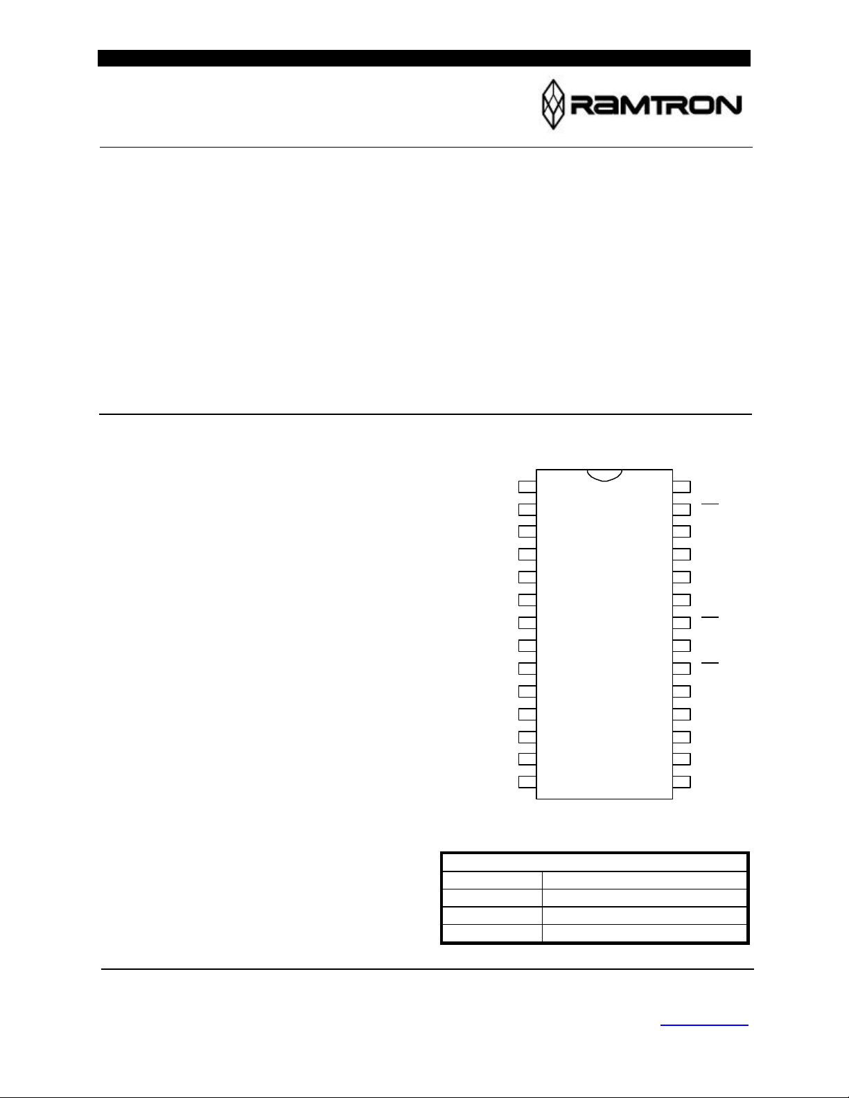
• 28-pin SOP or DIP
• Resistant to negative voltage undershoots
Description
The FM1808 is a 256-kilobit nonvolatile memory
Pin Configuration
employing an advanced ferroelectric process. A
ferroelectric random access memory or FRAM is
nonvolatile but operates in other respects as a RAM.
It provides data retention for 10 years while
eliminati ng the reliability concerns, functional
disadvantages and system design complexities of
battery -backed SRAM. It’s fast write and high write
endurance makes it superior to other types of
nonvolatile memory.
In-system operation of the FM1808 is very simila r to
A14
A12
A7
A6
A5
A4
A3
A2
VDD
WE
A13
A8
A9
A11
OE
A10
other RAM based devices. Memory read- and writecycles require equal times. The FRAM memory,
however, is nonvolatile due to its unique ferroelectric
memory process. Unlike BBSRAM, the FM1808 is a
truly monolithic nonvolatile memory. It provides the
same functional benefits of a fast write without the
serious disadvantages associated with modules and
batteries or hybrid memory solutions.
These capabilities make the FM1808 ideal for
nonvolatile memory applications requiring frequent or
rapid writes in a bytewide environment. The
availability of a true surface-mount package improves
the manufacturability of new designs, while the DIP
package facilitates simple design retrofits. The
FM1808 offers guaranteed operation over an
industrial temperature range of -40°C to +85°C.
A1
A0
DQ0
DQ1
DQ2
VSS DQ3
Ordering Information
FM1808-70-P 70 ns access, 28-pin plastic DIP
FM1808-70-S 70 ns access, 28-pin SOP
FM1808-120-P 120 ns access, 28-pin plastic DIP
FM1808-120-S 120 ns access, 28-pin SOP
CE
DQ7
DQ6
DQ5
DQ4
This data sheet contains design specifications for product development. Ramtron International Corporation
These specifications may change in any manner without notice. 1850 Ramtron Drive, Colorado Springs, CO 80921
(800) 545-FRAM, (719) 481-7000, Fax (719) 481-7058
www.ramtron.com
27 July 2000 1/12
Page 2
Ramtron FM1808-70
Figure 1. Block Diagram
A0-A14
Address
Latch
CE
WE
OE
Control
Logic
Pin Description
Pin Name Pin Number I/O Pin Description
A0-A14 1-10, 21, 23-26 I Address. The 15 address lines select one of 32,768 bytes in the FRAM
DQ0-7 11-13, 15-19 I/O Data. 8-bit bi -directional data bus for accessing the FRAM array.
/CE 20 I Chip Enable. /CE selects the device when low. The falling edge of /CE
/OE 22 I Output Enable. When /OE is low the FM1808 drives the data bus when
/WE 27 I Write Enable. Taking /WE low causes the FM1808 to write the contents
VDD 28 I Supply Voltage. 5V
VSS 14 I Ground.
Functional Truth Table
/CE /WE /OE Function
H X X Standby/Precharge
æ
X X Latch Address
L H L Read
L L X Write
A10-A14
A0-A7
A8-A9
Row
Decoder
1Kx8 1Kx8 1Kx81Kx8
1Kx8 1Kx8 1Kx81Kx8
1Kx8 1Kx8 1Kx81Kx8
1Kx8 1Kx8 1Kx81Kx8
1Kx8 1Kx8 1Kx81Kx8
1Kx8 1Kx8 1Kx81Kx8
1Kx8 1Kx8 1Kx81Kx8
1Kx8 1Kx8 1Kx81Kx8
Block Decoder
Column Decoder
I/O Latch
Bus Driver
DQ0-7
array. The address value will be latched on the falling edge of /CE.
causes the address to be latched internally. Address changes that
occur after /CE goes low will be ignored until the next falling edge
occurs.
valid data is available. Taking /OE high causes the DQ pins to be tristated.
of the data bus to the address location latched by the falling edge of
/CE.
27 July 2000 2/12
Page 3

Ramtron FM1808-70
Overview
The FM1808 is a bytewide FRAM memory. The
memory array is logically organized as 32,768 x 8 and
is accessed using an industry standard parallel
interface. The FM1808 is inherently nonvolatile via its
unique ferroelectric process. All data written to the
part is immediately nonvolatile with no delay.
Functional operation of the FRAM memory is similar
to SRAM type devices. The major operating
difference between the FM1808 and an SRAM
(beside nonvolatile storage) is that the FM1808
latches the address on the falling edge of /CE.
Memory Architecture
Users access 32,768 memory locations each with 8
data bits through a parallel interface. The complete
address of 15-bits specifies each of the 32,768 bytes
uniquely. Internally, the memory array is organized
into 32 blocks of 8Kb each. The 5 most-significant
address lines decode one of 32 blocks. This block
segmentation has no effect on operation, however the
user may wish to group data into blocks by its
endurance requirements as explained in a later
section.
The access and cycle time are the same for read and
write memory operations. Writes occur immediately at
the end of the access with no delay. Unlike an
EEPROM, it is not necessary to poll the device for a
ready condition since writes occur at bus speed. A
pre-charge operation, where /CE goes inactive, is a
part of every memory cycle. Thus unlike SRAM, the
access and cycle times are not equal.
Note that the FM1808 has no special power-down
demands. It will not block user access and it contains
no power-management circuits other than a simple
internal power-on reset. It is the user’s responsibility
to ensure that VDD is within data sheet tolerances to
prevent incorrect operation.
Memory Operation
The FM1808 is designed to operate in a manner very
similar to other bytewide memory products. For users
familiar with BBSRAM, the performance is comparable
but the bytewide interface operates in a slightly
different manner as described below. For users
familiar with EEPROM, the obvious differences result
from the higher write performance of FRAM
technology including NoDelay writes and much
higher write endurance.
27 July 2000 3/12
Read Operation
A read operation begins on the falling edge of /CE. At
this time, the addre ss bits are latched and a memory
cycle is initiated. Once started, a full memory cycle
must be completed internally even if /CE goes
inactive. Data becomes available on the bus after the
access time has been satisfied.
After the address has been latched, the address value
may be changed upon satisfying the hold time
parameter. Unlike an SRAM, changing address values
will have no effect on the memory operation after the
address is latched.
The FM1808 will drive the data bus when /OE is
asserted to a low state. If /OE is asserted after the
memory access time has been satisfied, the data bus
will be driven with valid data. If /OE is asserted prior
to completion of the memory access, the data bus will
not be driven until valid data is available. This feature
minimizes supply current in the system by eliminating
transients due to invalid data. When /OE is inactive
the data bus will remain tri-stated.
Write Operation
Writes occur in the FM1808 in the same time interval
as reads. The FM1808 supports both /CE and /WE
controlled write cycles. In all cases, the address is
latched on the falling edge of /CE.
In a /CE controlled write, the /WE signal is asserted
prior to beginning the memory cycle. That is, /WE is
low when /CE falls. In this case, the part begins the
memory cycle as a write. The FM1808 will not drive
the data bus regardless of the state of /OE.
In a /WE controlled write, the memory cycle begins on
the falling edge of /CE. The /WE signal falls after the
falling edge of /CE. Therefore, the memory cycle
begins as a read. The data bus will be driven
according to the state of /OE until /WE falls. The
timing of both /CE and /WE controlled write cycles is
shown in the electrical specifications.
Write access to the array begins asynchronously
after the memory cycle is initiated. The write access
terminates on the rising edge of /WE or /CE,
whichever is first. Data set-up time, as shown in the
electrical specifications, indicates the interval during
which data cannot change prior to the end of the write
access.
Unlike other truly nonvolatile memory technologies,
there is no write delay with FRAM. Since the read and
write access times of the underlying memory are the
same, the user experiences no delay through the bus.
Page 4
Ramtron FM1808-70
The entire memory operation occurs in a single bus
cycle. Therefore, any operation including read or write
can occur immediately following a write. Data polling,
a technique used with EEPROMs to determine if a
write is complete, is unnecessary.
Pre-charge Operation
The pre-charge operation is an internal condition
where the state of the memory is prepared for a new
access. All memory cycles consist of a memory
access and a pre-charge. The pre-charge is user
initiated by taking the /CE signal high or inactive. It
must remain high for at least the minimum pre -charge
timing specification.
The user dictates the beginning of this operation
since a pre-charge will not begin until /CE rises.
However, the device has a maximum /CE low time
specification that must be satisfied.
Endurance and Memory Architecture
Data retention is specified in the electrical
specifications below. This section elaborates on the
relationship between data retention and endurance.
FRAM offers substantially higher write endurance
than other nonvolatile memories. Above a certain
level, however, the effect of increasing memory
accesses on FRAM produces an increase in the soft
error rate. There is a higher likelihood of data loss but
the memory continues to function properly. This
effect becomes significant only after 100 million (1E8)
read/write cycles, far more than allowed by other
nonvolatile memory technologies.
Endurance is a soft specification. Therefore, the user
may operate the device with different levels of cycling
for different portions of the memory. For example,
critical data needing the highest reliability level could
be stored in memory locations that receive
comparatively few cycles. Data with frequent changes
or shorter-term use could be located in an area
receiving many more cycles. A scratchpad area,
needing little if any retention can be cycled virtually
without limit.
Internally, a FRAM operates with a read and restore
mechanism similar to a DRAM. Therefore, each cycle
be it read or write, involves a change of state. The
memory architecture is based on an array of rows and
columns. Each access causes an endurance cycle for
an entire row. Therefore, data locations targeted for
substantially differing numbers of cycles should not
be located within the same row. To balance the
endurance cycles and allow the user the maximum
27 July 2000 4/12
flexibility, the FM1808 employs a unique memory
organization as described below.
The memory array is divided into 32 blocks, each
1Kx8. The 5-upper address lines decode the block
selection as shown in Figure 2. Data targeted for
significantly different numbers of cycles should be
located in separate blocks since memory rows do not
extend across block boundaries.
Figure 2. Address Blocks
FFFFh
Block 31
FC00h
FBFFh
Block 30
F800h
F7FFh
Block 29
F400h
F3FFh
Block 28
F000h
Block 27
Block 4
Block 3
Block 2
Block 1
Block 0
Each block of 1Kx8 consists of 256 rows and 4
columns. The address lines A0-A7 decode row
selection and A8-A9 lines decode column selection.
This scheme facilitates a relatively uniform
distribution of cycles across the rows of a block. By
allowing the address LSBs to decode row selection,
the user avoids applying multiple cycles to the same
row when accessing sequential data. For example, 256
bytes can be accessed sequentially without accessing
the same row twice. In this example, one cycle would
be applied to each row. An entire block of 1Kx8 can
be read or written with only four cycles applied to
each row. Figure 3 illustrates the organization within a
memory block.
EFFFh
1000h
0FFFh
0C00h
0BFFh
0800h
07FFh
0400h
03FFh
0000h
Page 5

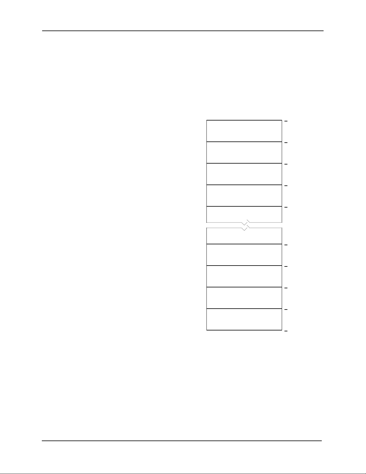
Ramtron FM1808-70
Figure 3. Row and Column Organization
A9-A8
11b
10b
Row 0
Row 1
Row 2
01b
Row 3
Row 253
Row 254
Row 252
Block 4
A14-A10
00100b
Row 255
qualified using HAST – highly accelerated stress test.
This requires 120º C at 85% Rh, 24.4 psia at 5.5V.
3. System reliability
Data integrity must be in question when using a
battery -backed SRAM. They are inherently
vulnerable to shock and vibration. If the battery
contact comes loose, data will be lost. In addition a
negative voltage, even a momentary undershoot, on
any pin of a battery-backed SRAM can cause data
loss. The negative voltage causes current to be drawn
00b
directly from the battery. These momentary short
circuits can greatly weaken a battery and reduce its
A0-A7 00h FFh
01h
02h 03h
FCh
FDh
FEh
capacity over time. In general, there is no way to
monitor the lost battery capacity. Should an
Applications
As the first truly nonvolatile RAM, the FM1808 fits
into many diverse applications. Clearly , its monolithic
nature and high performance make it superior to
battery -backed SRAM in most every application. This
applications guide is intended to facilitate the
transition from BBSRAM to FRAM. It is divided into
two parts. First is a treatment of the advantages of
FRAM memory compared with battery-backed
SRAM. Second is a design guide, which highlights
the simple design considerations that should be
reviewed in both retrofit and new design situations.
FRAM Advantages
Although battery-backed SRAM is a mature and
established solution, it has numerous weaknesses.
These stem, directly or indirectly from the presence of
the battery. FRAM uses an inherently nonvolatile
storage mechanism that requires no battery. It
therefore eliminates these weaknesses. The major
considerations in upgrading to FRAM are as follows.
Construction Issues
1. Cost
The cost of both the component and the
manufacturing overhead of battery -backed SRAM is
high. FRAM with its monolithic construction is
inherently a lower cost solution. In addition, there is
no ‘built-in’ rework step required for battery
attachment when using surface mount parts.
Therefore assembly is streamlined and more cost
effective. In the case of DIP battery -backed modules,
the user is constrained to through-hole assembly
techniques and a board wash using no water.
2. Humidity
A typical battery-backed SRAM module is qualified at
60º C, 90% Rh, no bias, and no pressure. This is
because the multi-component assemblies are
undershoot occur in a battery backed system during a
power down, data can be lost immediately.
4. Space
Certain disadvantages of battery-backed, such as
susceptibility to shock, can be reduced by using the
old fashioned DIP module. However, this alternative
takes up board space, height, and dictates throughhole assembly. FRAM offers a true surface-mount
solution that uses 25% of the board space.
No multi-piece assemblies, no connectors, and no
modules. A real nonvolatile RAM is finally
available!
Direct Battery Issues
5. Field maintenance
Batteries, no matter how mature, are a built-in
maintenance problem. They eventually must be
replaced. Despite long life projections, it is impossible
to know if any individual battery will last considering
all of the factors that can degrade them.
6. Environmental
Lithium batteries are widely regarded as an
environmental problem. They are a potential fire
hazard and proper disposal can be a burden. In
addition, shipping of lithium batteries may be
restricted.
7. Style!
Backing up an SRAM with a battery is an oldfashioned approach. In many cases, such modules are
the only through-hole component in sight. FRAM is
the latest memory technology and it is changing the
way systems are designed.
FRAM is nonvolatile and writes fast -- no battery
required!
vulnerable to moisture, not to mention dirt. FRAM is
27 July 2000 5/12
Page 6

Ramtron FM1808-70
FRAM Design Considerations
When designing with FRAM for the first time, users
of SRAM will recognize a few minor differences. First,
bytewide FRAM memories latch each address on the
falling edge of chip enable. This allows the address
bus to change after starting the memory access. Since
every access latches the memory address on the
falling edge of /CE, users should not ground it as they
might with SRAM.
Users that are modifying existing designs to use
FRAM should examine the hardware address
decoders. Decoders should be modified to qualify
addresses with an address valid signal if they do not
already. In many cases, this is the only change
required. Systems that drive chip enable active, then
inactive for each valid address may need no
modifications. An example of the target signal
relationships are shown in Figure 4. Also shown is a
common SRAM signal relationship that will not work
for the FM1808.
Figure 4. Memory Address Relationships
The main design issue is to create a decoder scheme
that will drive /CE active, then inactive for each
address. This accomplishes the two goals of latching
the new address and creating the precharge period.
A second design consideration relates to the level of
VDD during operation. Battery-backed SRAMs are
forced to monitor VDD in order to switch to battery
backup. They typically block user access below a
certain VDD level in order to prevent loading the
battery with current demand from an active SRAM.
The user can be abruptly cut off from access to the
nonvolatile memory in a power down situation with
no warning or indication.
FRAM memories do not need this system overhead.
The memory will not block access at any VDD level.
The user, however, should prevent the processor
from accessing memory when VDD is out-oftolerance. The common design practice of holding a
processor in reset when VDD drops is adequate; no
special provisions must be taken for FRAM design.
Signaling
Address
Data
Signaling
Address
Data
FRAM
Valid Memory Read Relationship
CE
A1 A2
D1 D2
SRAM
Invalid Memory Read Relationship
CE
A1 A2
D1 D2
27 July 2000 6/12
Page 7

Ramtron FM1808-70
Electrical Specifications
Absolute Maximum Ratings
Description Ratings
Ambient storage or operating temperature -40°C to + 85°C
Voltage on any pin with respect to ground -1.0V to +7.0V
Lead temperature (Soldering, 10 seconds) 300° C
Stresses above those listed under Absolute Maximum Ratings may cause permanent damage to the device. This is a
stress rating only, and the functional operation of the device at these or any other conditions above those listed in
the operational section of this specification is not implied. Exposure to absolute maximum ratings conditions for
extended periods may affect device reliability
DC Operating Conditions TA = -40° C to + 85° C, VDD = 4.5V to 5.5V unless otherwise specified
Symbol Parameter Min Typ Max Units Notes
VDD Power Supply 4.5 5.0 5.5 V 1
IDD VDD Supply Current 180 ns cycle 7 15 mA 2
IDD VDD Supply Current 120 ns cycle 12 25 mA 2
ISB Standby Current - TTL 400 µA 3
ISB Standby Current - CMOS 7 20 µA 4
ILI Input Leakage Current 10 µA 5
ILO Output Leakage Current 10 µA 5
VIL Input Low Voltage -1.0 0.8 V 1
VIH Input High Voltage 2.0 VDD + 1.0 V 1
VOL Output Low Voltage 0.4 V 1,6
VOH Output High Voltage 2.4V V 1,7
Notes
1. Referenced to VSS.
2. VDD = 5.5V, /CE cycling at minimum cycle time, 130 ns for –70 and 180 ns for -120. All inputs at CMOS levels, all
outputs unloaded.
3. VDD = 5.5V, /CE at VIH, All inputs at TTL levels, all outputs unloaded.
4. VDD = 5.5V, /CE at VIH, All inputs at CMOS levels, all outputs unloaded.
5. VIN, VOUT between VDD and VSS.
6. IOL = 4.2 mA
7. IOH = -2.0 mA
27 July 2000 7/12
Page 8

Ramtron FM1808-70
Read Cycle AC Parameters TA = -40° C to + 85° C, VDD = 4.5V to 5.5V unless otherwise specified
Symbol Parameter -70 -120 Units Notes
Min Max Min Max
tCE Chip Enable Access Time (to data valid) 70 120 ns
tCA Chip Enable Active Time 70 10,000 120 10,000 ns
tRC Read Cycle Time 130 180 ns
tPC Precharge Time 60 60 ns
tAS Address Setup Time 5 5 ns
tAH Address Hold Time 10 10 ns
tOE Output Enable Access Time 10 10 ns
tHZ Chip Enable to Output High-Z 15 15 ns 1
tOHZ Output Enable to Output High-Z 15 15 ns 1
Write Cycle AC Parameters TA = -40° C to + 85° C, VDD = 4.5V to 5.5V unless otherwise specified
Symbol Parameter -70 -120 Units Notes
Min Max Min Max
tCA Chip Enable Active Time 70 10,000 120 10,000 ns
tCW Chip Enable to Write High 70 120 ns
tWC Write Cycle Time 130 180 ns
tPC Precharge Time 60 60 ns
tAS Address Setup Time 0 0 ns
tAH Address Hold Time 10 10 ns
tWP Write Enable Pulse Width 40 40 ns
tDS Data Setup 30 40 ns
tDH Data Hold 5 5 ns
tWZ Write Enable Low to Output High Z 15 15 ns 1
tWX Write Enable High to Output Driven 10 10 ns 1
tHZ Chip Enable to Output High-Z 15 15 ns 1
tWS Write Setup 0 0 ns 2
tWH Write Hold 0 0 ns 2
Notes
1 This parameter is periodically sampled and not 100% tested.
2 The relationship between /CE and /WE determines if a /CE- or /WE-controlled write occurs. There is no timing
specification associated with this relationship.
Power Cycle Timing TA = -40° C to + 85° C, VDD = 4.5V to 5.5V unless otherwise specified
Symbol Parameter Min Units Notes
tPU VDD Min to First Access Start 1 µS
tPD Last Access Complete to VDD Min 0 µS
Capacitance TA = 25° C , f=1.0 MHz, VDD = 5V
Symbol Parameter Max Units Notes
CI/O Input Output Capacitance 8 pF
CIN Input Capacitance 6 pF
27 July 2000 8/12
Page 9

Ramtron FM1808-70
AC Test Conditions
Equivalent AC Load Circuit
Input Pulse Levels 0 to 3V
Input rise and fall times 10 nS
Input and output timing levels 1.5V
Read Cycle Timing
t
RC
t
CA
t
PC
CE
t
t
AH
AS
A0-17
t
OE
OE
t
OHZ
DQ0-7
t
CE
t
HZ
Write Cycle Timing - /CE Controlled Timing
t
WC
t
CA
t
PC
CE
t
t
AH
AS
A0-17
t
WS
t
WH
WE
OE
DQ0-7
t
DS
t
DH
27 July 2000 9/12
Page 10

Ramtron FM1808-70
Write Cycle Timing - /WE Controlled Timing
t
WC
t
CA
t
PC
CE
t
t
AH
AS
A0-17
t
WH
WE
t
WS
t
WP
OE
t
WZ
t
WX
DQ0-7
out
t
t
DS
DH
DQ0-7
in
Power Cycle Timing
VDD
VDD
min
t
PD
t
PC
VDD
min
t
PU
CE
Data Retention TA = -40° C to + 85° C, VDD = 4.5V to 5.5V unless otherwise specified
Parameter Min Units Notes
Data Retention 10 years 1
Notes
1. Data retention is specified at 85° C. The relationship between retention, temperature, and the associated
reliability level is characterized in a separate reliability report.
27 July 2000 10/12
Page 11

Ramtron FM1808-70
α
28-pin SOP JEDEC MS-013
Index
Area
E H
Pin 1
D
A
B
e
A1
.10 mm
.004 in.
h
45
L
C
Selected Dimensions
For complete dimensions and notes, refer to JEDEC MS -013
Controlling dimensions is in millimeters. Conversions to inches are
not exact.
Symbol Dim Min Nom. Max
A mm
in.
A1 mm
in.
B mm
in.
C mm
in.
D m m
in.
E mm
in.
e mm
in.
H mm
in.
h mm
in.
L mm
in.
2.35
2.65
0.0926
0.10
0.30
0.004
0.33
0.51
0.013
0.23
0.32
0.0091
17.70
18.10
0.6969
7.40
7.60
0.2914
1.27 BSC
10.00
0.050 BSC
10.65
0.394
0.25
0.75
0.010
.40
1.27
0.016
0.1043
0.0118
0.020
0.0125
0.7125
0.2992
0.419
0.029
0.050
α 0° 8°
27 July 2000 11/12
Page 12

Ramtron FM1808-70
28-pin DIP JEDEC MS-011
E1
Index
Area
D
A2 A
A1
D1
e
Selected Dimensions
For complete dimensions and notes, refer to JEDEC MS -011
Controlling dimensions is in inches. Conversions to millimeters are
not exact.
Symbol Dim Min Nom. Max
A in.
A1 in.
A2 in.
B in.
B1 in.
D in.
D1 in.
E in.
E1 in.
e in.
eA in.
eB in.
L in.
mm
mm
mm
mm
mm
mm
mm
mm
mm
mm
mm
mm
mm
b
B1
0.250
0.015
0.39
0.125
3.18
0.014
0.356
0.030
0.77
1.380
35.1
0.005
0.13
0.600
15.24
0.485
12.32
0.100 BSC
0.600 BSC
0.700
0.115
2.93
0.195
0.070
1.565
0.625
0.580
2.54 BSC
15.24 BSC
0.200
6.35
4.95
0.022
0.558
1.77
39.7
15.87
14.73
17.78
5.08
E
eA
eB
27 July 2000 12/12
 Loading...