

Page 1
FDB8444
N-Channel PowerTrench® MOSFET
40V, 70A, 5.5mΩ
FDB8444 N-Channel PowerTrench
February 2006
Features
Typ r
Typ Q
Low Miller Charge
Low Qrr Body Diode
UIS Capability (Single Pulse and Repetitive Pulse)
Qualified to AEC Q101
RoHS Compliant
= 3.9mΩ at VGS = 10V, ID = 70A
DS(on)
g(TOT)
= 91nC at V
GS
= 10V
Applications
Automotive Engine Control
Powertrain Management
Solenoid and Motor Drivers
Electronic Transmission
Distributed Power Architecture and VRMs
Primary Switch for 12V Systems
E
E
R
F
I
D
A
E
L
M
P
L
E
M
E
N
T
A
T
I
O
N
®
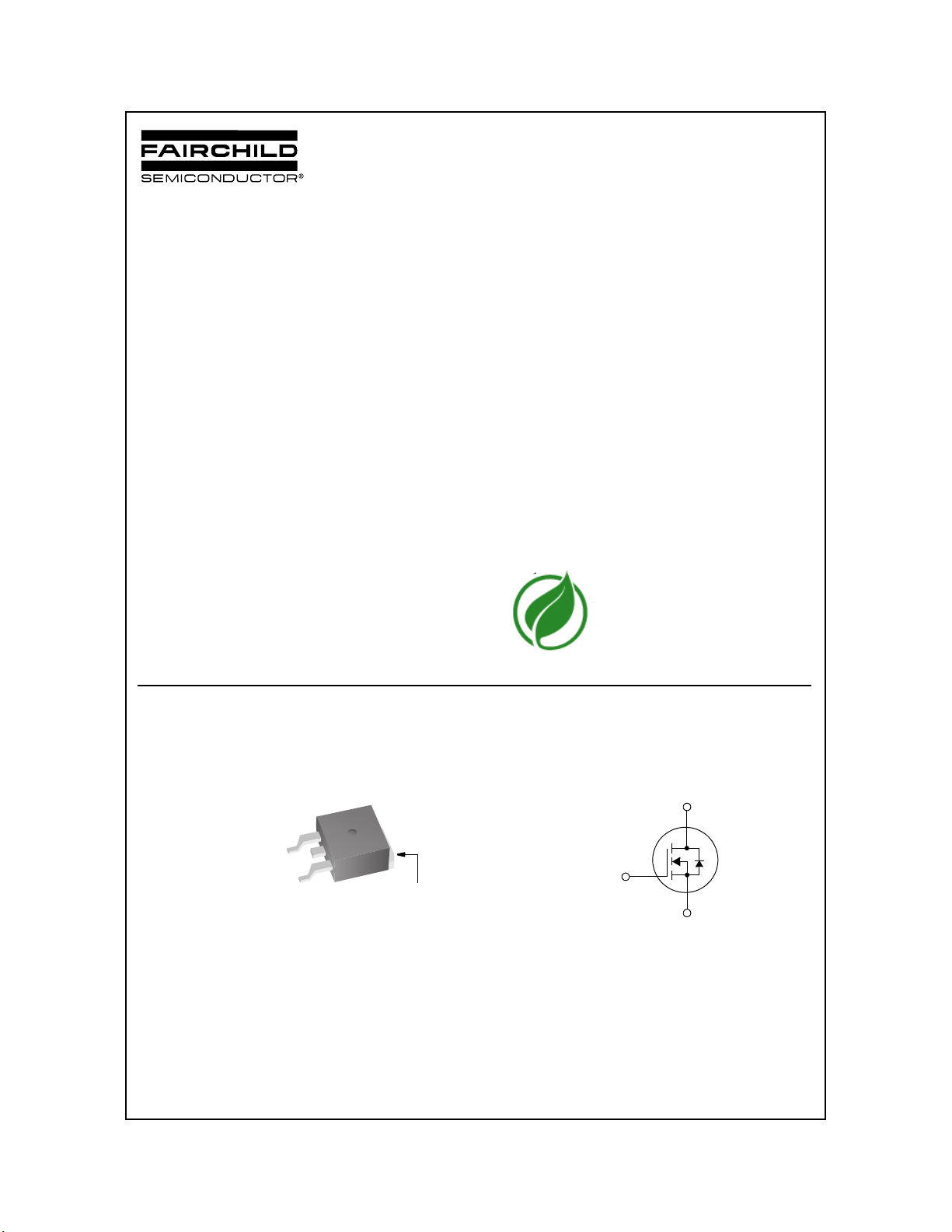
MOSFET
GATE
SOURCE
TO-263AB
FDB SERIES
©2006 Fairchild Semiconductor Corporation
FDB8444 Rev A2 (W)
D
G
DRAIN
(FLANGE)
S
www.fairchildsemi.com1
Page 2
Absolute Maximum Ratings T
= 25°C unless otherwise noted
C
Symbol Parameter Ratings Units
V
DSS
V
GS
I
D
E
AS
P
D
, T
T
J
STG
Drain to Source Voltage 40 V
Gate to Source Voltage ± 20 V
Drain Current Continuous (V
= 10V) (Note 1) 70 A
GS
Pulsed Figure 4
Single Pulse Avalanche Energy (Note 2) 307 mJ
Power Dissipation 167 W
o
Derate above 25
C1.1W/oC
Operating and Storage Temperature -55 to +175
Thermal Characteristics
R
θJC
R
θJA
Thermal Resistance, Junction to Case 0.9
Thermal Resistance, Junction to Ambient TO-263, lin2 copper pad area 43
Package Marking and Ordering Information
Device Marking Device Package Reel Size Tape Width Quantity
FDB8444 FDB8444 TO-263AB 330mm 24mm 800 units
o
C/W
o
C/W
FDB8444 N-Channel PowerTrench
o
C
®
MOSFET
Electrical Characteristics T
= 25°C unless otherwise noted
J
Symbol Parameter Test Conditions Min Typ Max Units
Off Characteristics
B
VDSS
I
DSS
I
GSS
On Characteristics
V
GS(th)
r
on)
DS(
Drain to Source Breakdown Voltage ID = 250µA, VGS = 0V 40 - - V
Zero Gate Voltage Drain Current
VDS = 32V
V
= 0V
GS
TJ =150°C - - 250
- - 1 µA
Gate to Source Leakage Current VGS = ±20V - - ±100 nA
Gate to Source Threshold Voltage VDS = VGS, ID = 250µA 2 2.6 4 V
ID = 70A, VGS = 10V - 3.9 5.5
Drain to Source On Resistance
ID = 70A, VGS = 10V,
TJ = 175°C
- 7 9.9
Dynamic Characteristics
C
iss
C
oss
C
rss
R
G
Q
g(TOT)
Q
g(TH)
Q
gs
Q
gs2
Q
gd
Input Capacitance
Output Capacitance - 480 640 pF
Reverse Transfer Capacitance - 290 435 pF
VDS = 25V, VGS = 0V,
f = 1MHz
- 6040 8035 pF
Gate Resistance f = 1MHz - 2 - Ω
Total Gate Charge at 10V VGS = 0 to 10V
Threshold Gate Charge VGS = 0 to 2V - 7 10 nC
Gate to Source Gate Charge
Gate Charge Threshold to Plateau - 17 - nC
VDD = 20V,
ID = 70A,
- 91 128 nC
- 23 - nC
Gate to Drain “Miller” Charge - 20 - nC
mΩ
FDB8444 Rev A2 (W)
www.fairchildsemi.com2
Page 3
Electrical Characteristics T
= 25°C unless otherwise noted
J
Symbol Parameter Test Conditions Min Typ Max Units
Switching Characteristics
t
(on)
t
d(on)
t
r
t
d(off)
t
f
t
off
Turn-On Time
- - 135 ns
Turn-On Delay Time - 12 - ns
Turn-On Rise Time - 78 - ns
Turn-Off Delay Time - 48 - ns
= 20V, ID = 70A
V
DD
= 10V, RGS = 2Ω
V
GS
Turn-Off Fall Time - 15 - ns
Turn-Off Time - - 95 ns
Drain-Source Diode Characteristics
I
= 70A - - 1.25 V
V
SD
t
rr
Q
rr
Notes:
1: Maximum wire current carrying capacity is 70A.
2: Starting T
Source to Drain Diode Voltage
Reverse Recovery Time IF = 70A, di/dt = 100A/µs--62ns
Reverse Recovery Charge IF = 70A, di/dt = 100A/µs--82nC
= 25oC, L = 0.2mH, IAS = 56A.
J
SD
= 35A - - 1.0 V
I
SD
FDB8444 N-Channel PowerTrench
®
MOSFET
This product has been designed to meet the extreme test conditions and environment demanded by the automotive industry. For
All Fairchild Semiconductor products are manufactured, assembled and tested under ISO9000 and QS9000 quality systems
FDB8444 Rev A2 (W)
a copy of the requirements, see AEC Q101 at: http://www.aecouncil.com/
certification.
www.fairchildsemi.com3
Page 4

Typical Characteristics
FDB8444 N-Channel PowerTrench
1.2
1.0
0.8
0.6
0.4
0.2
POWER DISSIPATION MULIPLIER
0.0
0 25 50 75 100 125 150 175
TC, CASE TEMPERATURE(oC)
Figure 1. Normalized Power Dissipation vs Case
Temperature
2
DUTY CYCLE - DESCENDING ORDER
1
D = 0.50
0.20
θJC
0.1
IMPEDANCE, Z
NORMALIZED THERMAL
0.01
0.10
0.05
0.02
0.01
SINGLE PULSE
-5
10
-4
10
-3
10
t, RECTANGULAR PULSE DURATION(s)
100
CURRENT LIMITED
BY WIRE
80
60
40
, DRAIN CURRENT (A)
20
D
I
0
25 50 75 100 125 150 175
Figure 2.
TC, CASE TEMPERATURE(oC)
Maximum Continuous Drain Current vs
Case Temperature
P
DM
NOTES:
DUTY FACTOR: D = t1/t
PEAK TJ = PDM x Z
-2
10
-1
10
θJC
x R
0
10
VGS = 10V
®
MOSFET
t
1
t
2
2
+ T
θJC
C
1
10
5000
1000
TRANSCONDUCTANCE
MAY LIMIT CURRENT
100
IN THIS REGION
, PEAK CURRENT (A)
DM
I
10
-5
10
SINGLE PULSE
FDB8444 Rev A2 (W)
VGS = 10V
Figure 3.
-4
10
Normalized Maximum Transient Thermal Impedance
TC = 25oC
FOR TEMPERATURES
ABOVE 25
CURRENT AS FOLLOWS:
I = I
25
-3
10
t, RECTANGULAR PULSE DURATION(s)
-2
10
-1
10
Figure 4. Peak Current Capability
o
C DERATE PEAK
175 - T
C
150
0
10
www.fairchildsemi.com4
1
10
Page 5

Typical Characteristics
FDB8444 N-Channel PowerTrench
1000
10us
100
100us
10
SINGLE PULSE
T
= MAX RATED
J
, DRAIN CURRENT (A)
1
D
I
0.1
1 10 100
o
T
= 25
C
C
OPERATION IN THIS
AREA MAY BE
LIMITED BY r
DS(on)
1ms
10ms
DC
VDS, DRAIN TO SOURCE VOLTAGE (V)
Figure 5.
140
120
Forward Bias Safe Operating Area
PULSE DURATION = 80µs
DUTY CYCLE = 0.5% MAX
V
= 5V
DD
100
80
60
40
, DRAIN CURRENT (A)
D
I
20
0
2.02.53.03.54.04.55.0
TJ = 175oC
TJ = 25oC
TJ = -55oC
VGS, GATE TO SOURCE VOLTAGE (V)
500
If R = 0
tAV = (L)(IAS)/(1.3*RATED BV
If R
≠
0
t
= (L/R)ln[(IAS*R)/(1.3*RATED BV
AV
100
10
STARTING TJ = 150oC
, AVALANCHE CURRENT (A)
AS
I
1
0.01 0.1 1 10 100 1000
NOTE: Refer to Fairchild Application Notes AN7514 and AN7515
tAV, TIME IN AVALANCHE (ms)
- VDD)
DSS
- VDD) +1]
DSS
STARTING TJ = 25oC
Figure 6. Unclamped Inductive Switching
Capability
140
120
100
80
60
40
, DRAIN CURRENT (A)
D
I
20
0
01234
V
= 10V
GS
VGS = 5V
VGS = 4.5V
PULSE DURATION = 80µs
DUTY CYCLE = 0.5% MAX
V
= 4V
GS
VGS = 3.5V
VDS, DRAIN TO SOURCE VOLTAGE (V)
®
MOSFET
Figure 7.
14
12
10
(mΩ)
8
6
, DRAIN TO SOURCE
ON-RESISTANCE
4
DS(on)
r
2
45678910
Figure 9.
Variation vs Gate to Source Voltage
FDB8444 Rev A2 (W)
Transfer Characteristics Figure 8.
I
= 70A
D
V
, GATE TO SOURCE VOLTAGE (V)
GS
PULSE DURATION = 80µs
DUTY CYCLE = 0.5% MAX
TJ = 175oC
TJ = 25oC
Drain to Source On-Resistance
2.0
1.8
1.6
1.4
1.2
NORMALIZED
1.0
0.8
0.6
DRAIN TO SOURCE ON-RESISTANCE
Figure 10.
Saturation Characteristics
PULSE DURATION = 80µs
DUTY CYCLE = 0.5% MAX
ID = 70A
V
= 10V
GS
-80 -40 0 40 80 120 160 200
TJ, JUNCTION TEMPERATURE(oC)
Normalized Drain to Source On
Resistance vs Junction Temperature
www.fairchildsemi.com5
Page 6

Typical Characteristics
FDB8444 N-Channel PowerTrench
1.2
1.1
1.0
0.9
0.8
0.7
0.6
NORMALIZED GATE
THRESHOLD VOLTAGE
0.5
0.4
-80 -40 0 40 80 120 160 200
Figure 11.
10000
1000
CAPACITANCE (pF)
100
0.1 1 10
V
= V
GS
DS
I
= 250µA
D
TJ, JUNCTION TEMPERATURE(oC)
Normalized Gate Threshold Voltage vs
Junction Temperature
C
ISS
C
OSS
C
f = 1MHz
V
= 0V
GS
VDS, DRAIN TO SOURCE VOLTAGE (V)
RSS
50
1.15
I
= 250µA
D
1.10
1.05
1.00
0.95
BREAKDOWN VOLTAGE
NORMALIZED DRAIN TO SOURCE
0.90
-80 -40 0 40 80 120 160 200
TJ, JUNCTION TEMPERATURE (oC)
Figure 12. Normalized Drain to Source
Breakdown Voltage vs Junction Temperature
10
ID = 70A
8
6
4
2
, GATE TO SOURCE VOLTAGE(V)
GS
0
V
020406080100
VDD = 15V
Q
, GATE CHARGE(nC)
g
VDD = 20V
VDD = 25V
®
MOSFET
Figure 13.
FDB8444 Rev A2 (W)
Capacitance vs Drain to Source
Voltage
Figure 14.
Gate Charge vs Gate to Source Voltage
www.fairchildsemi.com6
Page 7

TRADEMARKS
The following are registered and unregistered trademarks Fairchild Semiconductor owns or is authorized to use and is not
intended to be an exhaustive list of all such trademarks.
ACEx™
ActiveArray™
Bottomless™
Build it Now™
CoolFET™
CROSSVOLT™
DOME™
EcoSPARK™
2
CMOS™
E
EnSigna™
FACT™
FACT Quiet Series™
Across the board. Around the world.™
The Power Franchise
®
Programmable Active Droop™
®
FAST
FASTr™
FPS™
FRFET™
GlobalOptoisolator™
GTO™
HiSeC™
2
C™
I
i-Lo™
ImpliedDisconnect™
IntelliMAX™
ISOPLANAR™
LittleFET™
MICROCOUPLER™
MicroFET™
MicroPak™
MICROWIRE™
MSX™
MSXPro™
OCX™
OCXPro™
OPTOLOGIC
®
OPTOPLANAR™
PACMAN™
POP™
Power247™
PowerEdge™
PowerSaver™
PowerTrench
QFET
®
®
QS™
QT Optoelectronics™
Quiet Series™
RapidConfigure™
RapidConnect™
µSerDes™
ScalarPump™
SILENT SWITCHER
SMART START™
SPM™
Stealth™
SuperFET™
SuperSOT™-3
SuperSOT™-6
SuperSOT™-8
SyncFET™
TCM™
TinyLogic
TINYOPTO™
TruTranslation™
UHC™
UltraFET
UniFET™
®
VCX™
Wire™
®
®
DISCLAIMER
FAIRCHILD SEMICONDUCTOR RESERVES THE RIGHT TO MAKE CHANGES WITHOUT FURTHER NOTICE TO ANY
PRODUCTS HEREIN TO IMPROVE RELIABILITY, FUNCTION OR DESIGN. FAIRCHILD DOES NOT ASSUME ANY
LIABILITY ARISING OUT OF THE APPLICATION OR USE OF ANY PRODUCT OR CIRCUIT DESCRIBED HEREIN;
NEITHER DOES IT CONVEY ANY LICENSE UNDER ITS PATENT RIGHTS, NOR THE RIGHTS OF OTHERS.
FDB8444 N-Channel PowerTrench
®
MOSFET
LIFE SUPPORT POLICY
FAIRCHILD’S PRODUCTS ARE NOT AUTHORIZED FOR USE AS CRITICAL COMPONENTS IN LIFE SUPPORT DEVICES
OR SYSTEMS WITHOUT THE EXPRESS WRITTEN APPROVAL OF FAIRCHILD SEMICONDUCTOR CORPORATION.
As used herein:
1. Life support devices or systems are devices or systems
which, (a) are intended for surgical implant into the body, or
(b) support or sustain life, or (c) whose failure to perform
when properly used in accordance with instructions for use
provided in the labeling, can be reasonably expected to result
in significant injury to the user.
2. A critical component is any component of a life support
device or system whose failure to perform can be reasonably
expected to cause the failure of the life support device or
system, or to affect its safety or effectiveness.
PRODUCT STATUS DEFINITIONS
Definition of Terms
Datasheet Identification Product Status Definition
Advance Information Formative or In
Design
Preliminary First Production This datasheet contains preliminary data, and
No Identification Needed Full Production This datasheet contains final specifications. Fairchild
This datasheet contains the design specifications for
product development. Specifications may change in
any manner without notice.
supplementary data will be published at a later date.
Fairchild Semiconductor reserves the right to make
changes at any time without notice in order to improve
design.
Semiconductor reserves the right to make changes at
any time without notice in order to improve design.
Obsolete Not In Production This datasheet contains specifications on a product
that has been discontinued by Fairchild semiconductor.
The datasheet is printed for reference information only.
Rev. I18
FDB8444 Rev A2 (W)
www.fairchildsemi.com7
 Loading...