

Page 1
Features
■
2.3mA supply current
■
200MHz unity-gain bandwidth
■
2400V/µs slew rate
■
Unity gain stable
■
110dB common-mode rejection ratio
■
80mA drive current
■
>20Vppoutput swing
■
±5V to ±15V supplies
Applications
■
Video line driver
■
Video ADC driver
■
Desktop Multimedia
■
Low powered cable driver
■
Video DAC buffer
■
Active filters/integrators
■
NTSC & PAL video systems
General Description
The Comlinear CLC436 is a high-performance, low power,
voltage-feedback operational amplifier that has been designed
for a wide range of low-cost applications. The CLC436 is
specified to operate from dual ±5V to dual ±15V power supplies.
Operating from ±5V supplies, the unity gain stable CLC436
consumes a mere 23mW of power and features a 150MHz
bandwidth and 850V/µs slew rate. Operating from ±15V power
supplies, the CLC436 consumes only 69mW (Icc= 2.3mA) to
provide a 200MHz unity-gain bandwidth, a very fast 2400V/µs
slew rate and 13ns rise/fall times (5V step). At ±15V, the device
also provides large signal swings (>20Vpp) to give high dynamic
range and signal-to-noise ratio.
As a low-power NTSC or PAL video line-driver, the CLC436
delivers low differential gain and phase errors (0.2%, 1.2°) and
very high output drive current of 80mA. When used as a video
ADC driver, the CLC436 offers low Total Harmonic Distortion
(THD) and high Spurious Free Dynamic Range (SFDR).
Because of it’s voltage feedback topology, the CLC436
allows use of reactive elements in the feedback path and can
be configured as an excellent active filter for videoreconstruction DACs.
The CLC436’s combination of low cost and high performance in
addition to its low-power voltage-feedback topology make it a
versatile signal conditioning building block for a wide range
of price-sensitive applications.
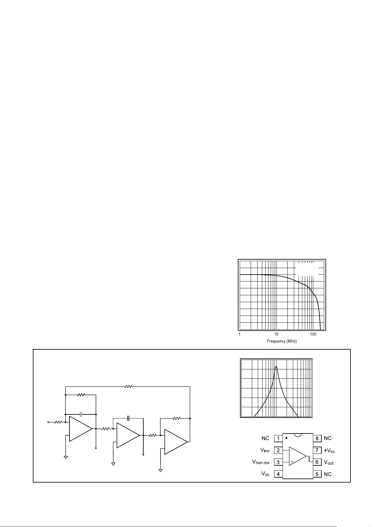
Frequency Response (Av = +2V/V)
V
out
= 0.5Vpp
V
cc
= ±15V
R
L
= 1kΩ
Magnitude (1dB/div)
C
120pF
Bandpass
Output
V
in
R
1
6631Ω
R
3
1326Ω
-
+
CLC436
R
4
3315Ω
-
+
CLC436
R
2
1326Ω
C
120pF
Low-pass
Output
-
+
CLC436
R
500Ω
R
500Ω
Typical Application
State-Variable Filter (1MHz, Q = 5, G = 2)
Pinout
DIP & SOIC
Bandpass Output
Magnitude (dB)
Frequency (MHz)
10
5
-20
0.1
1
10
0
-5
-10
-15
Comlinear CLC436
200MHz, ±15V, Low-Power Voltage Feedback Op Amp
August 1996
Comlinear CLC436
200MHz, ±15V, Low-Power Voltage Feedback Op Amp
N
© 1996 National Semiconductor Corporation http://www.national.com
Printed in the U.S.A.
Page 2
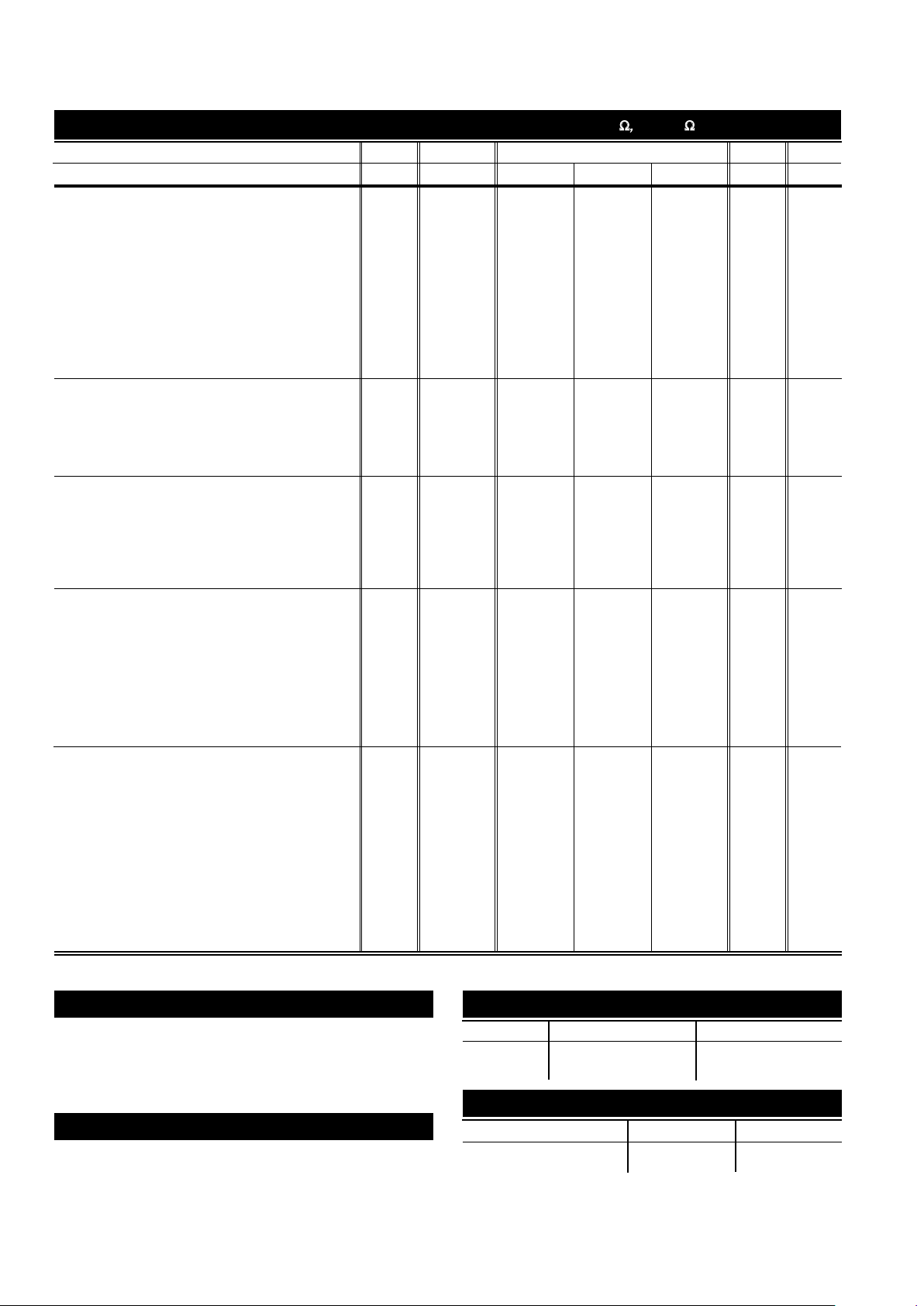
PARAMETERS CONDITIONS V
cc
TYP MIN/MAX RATINGS UNITS NOTES
CLC436AJ 25° 25° 0° to +70° -40° to +85°
FREQUENCY DOMAIN RESPONSE
-3dB bandwidth V
out
< 0.5V
pp
(AJP) ±15, ±5 96,55 50 50 50 MHz B
V
out
< 0.5V
pp
(AJE) ±15, ±5 96,55 50 60 40 MHz B
V
out
< 10V
pp
25 21 20 16 MHz
-3dB bandwidth A
V
= +1 V
out
< 0.5Vpp, Rf = 0 ±15, ±5 200,150 MHz
gain flatness V
out
< 0.5V
pp
rolloff DC to 20MHz 0.6 1.2 1.2 1.2 dB B
peaking DC to 10MHz 0 0.03 0.03 0.03 dB B
linear phase deviation DC to 10MHz 0.5 deg
differential gain 4.43MHz, R
L
=150Ω 0.2 %
differential phase 4.43MHz, R
L
=150Ω 1.2 deg
gain bandwidth product V
out
< 2.0V
pp
±15, ±5 200,100 MHz
TIME DOMAIN RESPONSE
rise and fall time 2V step, t
r
(in) = 5ns 11 13 14 18 ns
5V step, t
r
(in) = 5ns 13 16 18 20 ns
settling time to 0.05% 2V step, t
r
(in) = 5ns ±15, ±5 36,48 42 65 85 ns
overshoot 2V step, t
r
(in) = 5ns 0.5 1 2 2 %
slew rate 5V step, t
r
(in) = 5ns ±15, ±5 2400,850 2000 1900 1600 V/µs
DISTORTION AND NOISE RESPONSE
2
nd
harmonic distortion 1V
pp,
1MHz -72 -65 -62 -62 dBc
3
rd
harmonic distortion 1V
pp,
1MHz -70 -62 -60 -60 dBc
2
nd
harmonic distortion 1V
pp,
5MHz -65 -56 -56 -53 dBc B
3
rd
harmonic distortion 1V
pp,
5MHz -63 -54 -54 -54 dBc B
input voltage noise @1kHz 11 12.6 13.5 14.1 nV/√Hz
current noise @1kHz 0.8 1.5 1.9 2.3 pA/√Hz
STATIC DC PERFORMANCE
input offset voltage ±15, ±5 1.5,1.5 5 5 5 mV A
average drift 6 – 40 70 µV/˚C
input bias current ±15, ±5 1,1.2 3 3 4 µAA
average drift 4 – 50 70 nA/˚C
input offset current ±15, ±5 0.1,0.1 1 1 3 µAA
power supply rejection ratio DC 95 75 75 75 dB B
common-mode rejection ratio DC 110 75 73 70 dB
supply current R
L
= ∞ 2.3 4 4 4 mA A
open loop gain ±15, ±5 85,80 dB
MISCELLANEOUS PERFORMANCE
input resistance common-mode 40 20 15 10 MΩ
input capacitance common-mode 2 3 3 5 pF
input resistance differential-mode 4.9 4.0 3.0 2.5 MΩ
input voltage range common-mode ±15 ±12 ±11 ±10.5 ±10 V
input voltage range common-mode ±5 ±3 V
output voltage range R
L
= 100Ω ±15 +11.6/-10.5 +8.5/-8.5 +8.5/-8.5 +8.5/-8.5 V
R
L
= ∞ ± 15 +13/-12.2 +12/-12 +12/-12 +12/-12 V
output voltage range R
L
= 100Ω ±5 ±2.8 V
R
L
= ∞ ±5 ±3.4 V
output resistance, closed loop 0.01 0.05 0.07 0.1 Ω
output current sourcing ±15, ±5 120,90 100 95 90 mA
output current sinking ±15, ±5 80,40 75 70 65 mA
CLC436 Electrical Characteristics
(Vcc= ±15V, Av= +2, Rf= 499
W,
RL= 1kW; unless specified)
Absolute Maximum Ratings
supply voltage
±
18.0V
maximum junction temperature +150˚C
storage temperature range -65˚C to +150˚C
lead temperature (soldering 10 sec) +260˚C
Ordering Information
Model Temperature Range Description
CLC436AJP -40˚C to +85˚C 8-pin PDIP
CLC436AJE -40˚C to +85˚C 8-pin SOIC
Notes
A) J-level: spec is 100% tested at +25˚C, sample tested at +85˚C.
B)J-level: spec is sample tested at +25˚C.
Package Thermal Resistance
Package θ
JC
θ
JA
Plastic (AJP) 90°C/W 105°C/W
Surface Mount (AJE) 120°C/W 140°C/W
http://www.national.com 2
Min/max ratings are based on product characterization and simulation. Individual parameters are tested as noted. Outgoing quality levels are
determined from tested parameters.
Page 3

CLC436 Typical Performance Characteristics
(Vcc= ±15V, Av= +2, Rf= 499
W,
RL= 1kW; unless specified)
Non-Inverting Frequency Response
Magnitude (1dB/div)
Frequency (MHz)
1
10
100
Phase (deg)
0
-90
-360
-180
-270
-450
Av = 1
Av = 1
Av = 2
Av = 2
Av = 5
Av = 5
V
out
= 2V
pp
Inverting Frequency Response
Magnitude (1dB/div)
Frequency (MHz)
1
10
100
Phase (deg)
0
-90
-360
-180
-270
-450
Av = -2
V
out
= 2V
pp
Av = -1
Av = -1
Av = -2
Av = -5
Av = -5
Frequency Response vs. Load
Magnitude (1dB/div)
Frequency (MHz)
1
10
100
Phase (deg)
0
-90
-360
-180
-270
-450
RL = 1kΩ
V
out
= 2V
pp
RL = 1kΩ
RL = 100Ω
RL = 100Ω
RL = 50Ω
RL = 50Ω
Frequency Response vs. V
out
Magnitude (1dB/div)
Frequency (MHz)
1
10
100
Phase (deg)
0
-90
-360
-180
-270
-450
0.2V
pp
Av = 2V/V
0.5V
pp
2V
pp
5V
pp
Frequency Response vs. C
L
Magnitude (1dB/div)
Frequency (MHz)
1 10 100
+
-
R
s
1k
C
L
499Ω
499Ω
CLC436
CL=10pF
CL=33pF
CL=100pF
CL=1000pF
Open Loop Gain and Phase
Gain (dB)
Frequency (MHz)
-20
0
20
40
60
80
100
0.001 0.01 0.1 1 10 100
1000
Phase (deg)
-180
0
-90
Recommended Rs vs. C
L
R
s
(Ω)
Load Capacitance CL (pF)
10
20
30
40
50
60
100 300 500 700 900
+
-
R
s
1k
C
L
499Ω
499Ω
CLC436
Gain Flatness & Linear Phase
Magnitude (dB)
Frequency (MHz)
-0.5
-0.4
-0.3
-0.2
-0.1
0
0.1
0.2
0.3
0.4
0.5
0246810
Gain
Phase (deg)
-25
-20
-15
-10
-5
0
Phase
V
out
= 2V
pp
Equivalent Input Noise
Voltage Noise (nV/√Hz)
Frequency (MHz)
100
0
0.0001 0.001 0.01 0.1 1 10
10
Voltage = 11nV/√Hz
Current Noise pA/√Hz)
10
0.1
1
Current = 0.8pA/√Hz
2nd Harmonic Distortion vs. Frequency
Distortion (dBc)
Frequency (MHz)
-40
-50
1
10
-60
-70
V
out
= 2V
pp
RL = 100Ω
V
cc
= ±5V
RL = 100Ω
V
cc
= ±15V
RL = 1kΩ
V
cc
= ±15V
RL = 1kΩ
V
cc
= ±5V
-80
3rd Harmonic Distortion vs. Frequency
Distortion (dBc)
Frequency (MHz)
-40
-50
1
10
-60
-70
V
out
= 2V
pp
RL = 100Ω
V
cc
= ±5V
RL = 100Ω
V
cc
= ±15V
RL = 1kΩ
V
cc
= ±5V
RL = 1kΩ
V
cc
= ±15V
Differential Gain and Phase
Gain (%)
Number of 150Ω Loads
1.2
1.0
0.2
1
2
4
0.8
0.6
Phase Pos
Sync
Phase (deg)
3.0
2.5
1.0
2.0
1.5
0.4
Phase Neg
Sync
Gain Pos
Sync
Gain Neg
Sync
3
3.5
Large Signal Pulse Response
Output Voltage (2V/div)
Time (20ns/div)
Vo = 5V
pp
Small Signal Pulse Response
Output Voltage (0.5V/div)
Time (20ns/div)
Vo = 2V
pp
PSRR and CMRR
PSRR/CMRR (dB)
Frequency (MHz)
10
50
70
90
110
0.001 0.01 100
30
0.1 1 10
CMRR
PSRR
3 http://www.national.com
Page 4

CLC436 Typical Performance Characteristics
(Vcc= ±15V, Av= +2, Rf= 499
W,
RL= 1kW; unless specified)
CLC436 OPERATION
Description
The CLC436 is a unity gain stable voltage feedback
amplifier. The voltage feedback topology allows for
capacitors and nonlinear devices in the feedback path.
The matched input bias currents track well over
temperature. This allows the DC offset to be minimized
by matching the impedance seen by both inputs.
The low cost, low power, conventional topology, and
high output current make the CLC436 an excellent
choice for applications such as:
•
Low Power Cable Drivers
•
Active Filters
•
Buffers
•
NTSC and PAL Video Systems
Gain
The non-inverting and inverting gain equations for the
CLC436 are as follows:
Non-inverting Gain:
Inverting Gain:
Where Rfis the feedback resistor and Rgis the gain
setting resistor. Figure 1 shows the general noninverting gain configuration including the recommended
bypass capacitors.
Figure 1: Recommended Non-Inverting Gain Circuit
Output Drive Performance
The CLC436 can source over 120mA of output current.
It can easily drive 9Vppinto a 50Ω load. The circuit
shown in Figure 1 demonstrates the output current
capability of the CLC436. The circuit values listed
below, a 3Vppinput signal and ±15V supplies, were
used to obtain the result shown in Figure 2.
•
Rf= 499Ω
•
RL= 50Ω
•
Rg= 249.5Ω
•
Rin= 50Ω
Figure 2: Large Signal Pulse Response into 50
W
The high output drive capability of the CLC436 is
suitable for driving capacitive loads. When driving a
capacitive load or coaxial cable, include a series
resistance Rsto improve stability. Refer to the
Rsvs
Capacitive Load
plot in the typical performance
section to determine the recommended resistance for
various capacitive loads.
Single Supply Operation
The CLC436 can be operated from a single supply
using the topology shown in Figure 3. R1and R2form
a voltage divider that sets the non-inverting input
DC voltage. The coupling capacitor C1 isolates the
DC bias point from the previous stage. The DC gain
of this circuit is 1 and the high frequency gain is set by
Rfand Rg.
Power Derating Curves
Power (W)
Ambient Temperature (°C)
20
60
100
0 40 80 120
0
0.2
0.4
0.6
0.8
1.0
140 160 180
AJP
AJE
IBI, IOS, VIO vs. Temperature
Offset Voltage V
IO
(mV)
Temperature (°C)
0
-40
20
80
V
IO
I
BI
, I
OS
(µA)
0
0.5
0.2
1.0
0.4
1.5
0.6
2.0
0.8
2.5
1.0
3.0
1.2
-20 0 40 60
I
BI
I
OS
IBI & IOS vs. Common Mode Input Voltage
I
OS
(nA)
Common Mode Input Voltage
80
-10 -5 0 5 10
I
BI
(µA)
0
100
0.5
120
1.0
140
1.5
160
2.0
180
2.5
I
BI
I
OS
+
-
CLC436
R
f
0.1µF
6.8µF
V
o
V
in
+V
cc
0.1µF
6.8µF
-V
cc
R
L
R
g
R
in
gp
V
out
(V)
Time (100ns/div)
-5
Current (mA)
-100
-4
-80
-3
-60
-2
-40
-1
-20
0
0
1
20
2
40
3
60
4
80
5
100
Vin = 3Vpp
V
out
= 9V
pp
1
R
R
f
g
+
−
R
R
f
g
http://www.national.com 4
Page 5

Figure 3: Single Supply Circuit
Power Dissipation
The power dissipation of an amplifier can be described
in two conditions:
•
Quiescent Power Dissipation - P
Q
(No Load Condition)
•
Total Power Dissipation - P
T
(with Load Condition)
The following steps can be taken to determine the
power consumption of the CLC436:
1. Determine the quiescent power
PQ= Icc(V
cc
- Vee)
2. Determine the RMS power at the output stage
PO= (Vcc- V
load
) (I
load
)
3. Determine the total RMS power
PT= PQ+ P
O
The maximum power that the package can dissipate at
a given temperature is illustrated in the
Power Derating
plot in the
Typical Performance Characteristics
section. The power derating curve for any package
can be derived by utilizing the following equation:
where: T
amb
= Ambient temperature in °C
θJA= Thermal resistance, from junction to
ambient, for a given package in °C/W
Layout Considerations
A proper printed circuit layout is essential for achieving
high frequency performance. Comlinear provides evaluation boards for the CLC436 (730013 - DIP, 730027SOIC) and suggests their use as a guide for high
frequency layout and as an aid for device testing and
characterization.
Supply bypassing is required for optimum performance.
The bypass capacitors provide a low impedance
current return path at the supply pins. They also provide
high frequency filtering on the power supply traces.
Other layout factors also play a major role in high
frequency performance. The following steps are
recommended as a basis for high frequency layout:
1. Include 6.8µF tantalum and 0.01µF ceramic
bypass capacitors on both supplies.
2. Place the 6.8µF capacitors within 0.75 inches
of the power pins.
3. Place the 0.01µF capacitors within 0.1 inches
of the power pins.
4. Remove the ground plane near the input and
output pins to reduce parasitic capacitance.
5. Minimize all trace lengths to reduce series
inductances.
State Variable Filter
The filter shown on the front page offers both a bandpass and a low pass output. The design equations are
shown below.
The state variable filter can be modified to obtain a
tunable band pass filter. This technique is shown in
the CLC522, Wideband Variable Gain Amplifier,
data sheet.
Transimpedance Application
The low 1.1pA/√Hz input current noise and unity gain
stability make the CLC436 useful as a photo diode preamplifier. Figure 4 illustrates a transimpedance amplifier.
Rfsets the transimpedance gain. The photodiode current
is multiplied by Rfto determine the output voltage.
Figure 4: Transimpedance Amplifier
The feedback capacitor (Cf) is required to compensate
for the added input capacitance of the photodiode (Cd).
The feedback capacitance reduces peaking in the frequency response. As the value of the feedback capacitance increases from zero, the rolloff of the response
will increase.
P
175 T
amb
JA
=
°−
()
θ
Q
R
R
A
R
R
,desired mid band gain
f
Q
2RC
,desired resonant frequency
RR
1
3
v
1
4
r
1
23
=
=−
=
=
π
+
-
CLC436
R
f
V
o
V
in
V
cc
R
g
R
2
R
1
V
cc
C
1
C
2
Applications Circuit
I
in
-
+
CLC436
C
d
R
f
C
f
Photo Diode
Representation
Vo = I
in
*
R
f
V
o
5 http://www.national.com
Page 6

Instrumentation Amplifier
An instrumentation circuit is shown in Figure 5. The
high CMRR of the CLC436 benefits this application.
The resistors are kept equal to improve the overall
CMRR.
Figure 5: Instrumentation Amplifier
2nd Order Sallen-Key Band-Pass Filter
The CLC436 is well suited for Sallen-Key type active
filters. Figure 6 illustrates the band pass topology
and design equations. For optimum high frequency
performance:
•
Keep the resistor values between 10Ω and 1kΩ
•
Keep the capacitor values between 10pF
and 500pF
Begin design by choosing reasonable values for C
1
and C2and then setting the desired mid-band gain.
Figure 6: Sallen-Key Active Filter
V
1
500Ω
500Ω
+
-
500Ω
CLC436
500Ω
-
+
500ΩR
1
CLC436
50Ω
-
+
CLC436
500Ω
500Ω
V
2
Vo = 3(V2-V1)
R
f
R
g
R
3
CLC436
R
1
V
in
V
o
R
2
C
2
C
1
+
-
C
1
5
C
G1
R
R
, desired mid band gain
R2
Q
GC 2 f
, where f desiredcenter frequency
R
GR 1 4.8Q 2G G 1
4.8Q 2G G
R
5GR 1 4.8Q 2G G G 1
4Q
21
f
g
1
1
2
1
22
22
3
1
22
2
=
=+ −
=
()
=
=
+−++
−+
=
+−++−
π
Comlinear CLC436
200MHz, ±15V, Low-Power Voltage Feedback Op Amp
http://www.national.com 6 Lit #150436-004
Customer Design Applications Support
National Semiconductor is committed to design excellence. For sales, literature and technical support, call the
National Semiconductor Customer Response Group at 1-800-272-9959 or fax 1-800-737-7018.
Life Support Policy
National’s products are not authorized for use as critical components in life support devices or systems without the express written approval
of the president of National Semiconductor Corporation. As used herein:
1. Life support devices or systems are devices or systems which, a) are intended for surgical implant into the body, or b) support or
sustain life, and whose failure to perform, when properly used in accordance with instructions for use provided in the labeling, can
be reasonably expected to result in a significant injury to the user.
2. Acritical component is any component of a life support device or system whose failure to perform can be reasonably expected to
cause the failure of the life support device or system, or to affect its safety or effectiveness.
National Semiconductor National Semiconductor National Semiconductor National Semiconductor
Corporation Europe Hong Kong Ltd. Japan Ltd.
1111 West Bardin Road Fax: (+49) 0-180-530 85 86 13th Floor, Straight Block Tel: 81-043-299-2309
Arlington, TX 76017 E-mail: europe.support.nsc.com Ocean Centre, 5 Canton Road Fax: 81-043-299-2408
Tel: 1(800) 272-9959 Deutsch Tel: (+49) 0-180-530 85 85 Tsimshatsui, Kowloon
Fax: 1(800) 737-7018 English Tel: (+49) 0-180-532 78 32 Hong Kong
Francais Tel: (+49) 0-180-532 93 58 Tel: (852) 2737-1600
Italiano Tel: (+49) 0-180-534 16 80 Fax: (852) 2736-9960
National does not assume any responsibility for use of any circuitry described, no circuit patent licenses are implied and National reserves the right at any time without notice to change said
circuitry and specifications.
N
 Loading...