

Page 1
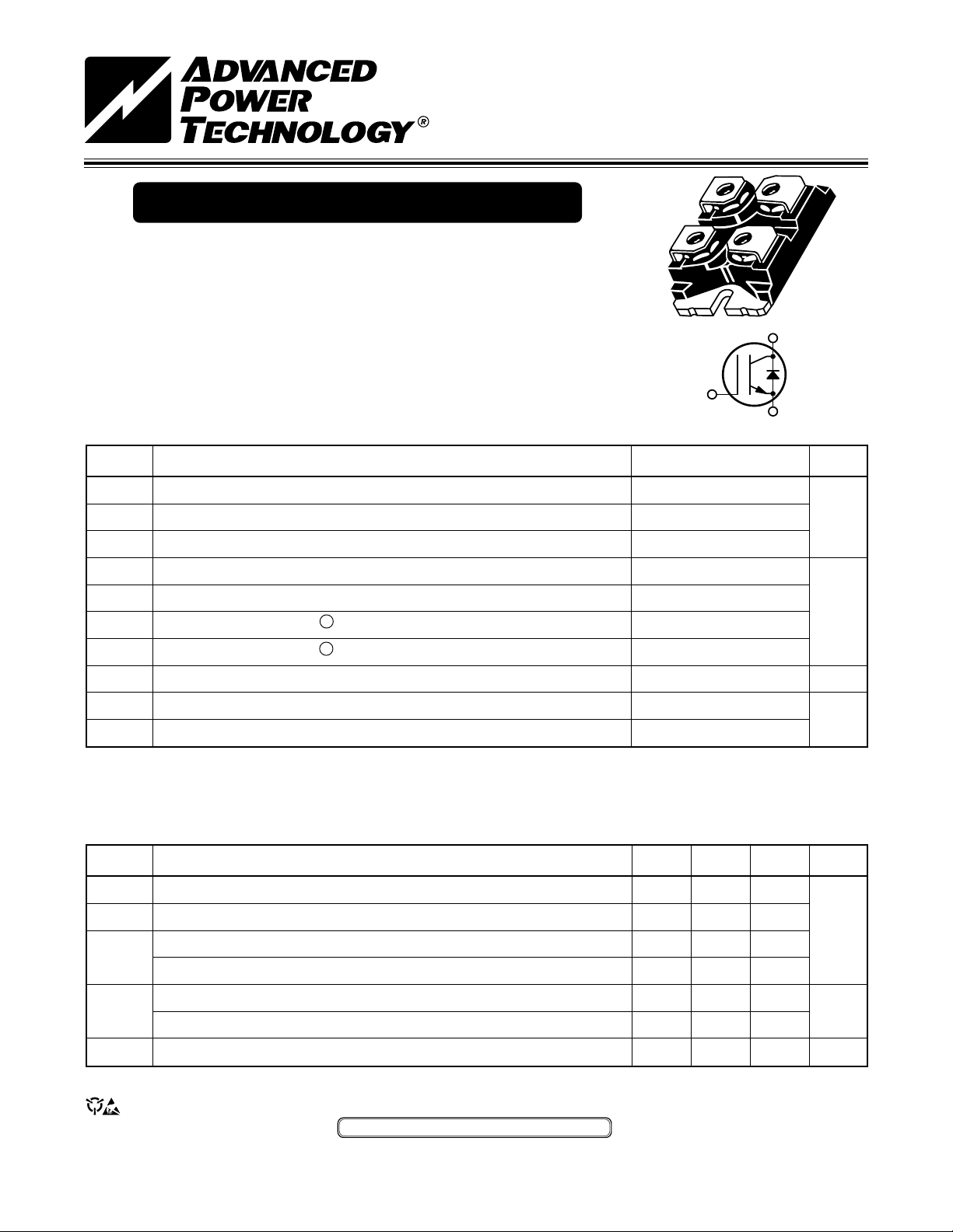
APT60GT60JRD
SOT-227
G
E
E
C
ISOTOP
®
"UL Recognized"
Thunderbolt IGBT™ & FRED
The Thunderbolt IGBT™ is a new generation of high voltage power IGBTs.
Using Non-Punch Through Technology the Thunderbolt IGBT™ combined
with an APT free-wheeling ultraFast Recovery Epitaxial Diode (FRED) offers
superior ruggedness and ultrafast switching speed.
600V 90A
• Low Forward Voltage Drop • High Freq. Switching to 150KHz
C
• Low Tail Current • Ultra Low Leakage Current
• Ultrafast Soft Recovery • RBSOA and SCSOA Rated
G
Antiparallel Diode
E
MAXIMUM RATINGS (IGBT) All Ratings: TC = 25°C unless otherwise specified.
Symbol
V
CES
V
CGR
V
GE
I
C1
I
C2
I
CM1
I
CM2
P
D
TJ,T
STG
T
L
Parameter
Collector-Emitter Voltage
Collector-Gate Voltage (R
Gate-Emitter Voltage
Continuous Collector Current @ T
Continuous Collector Current @ T
Pulsed Collector Current
Pulsed Collector Current
Total Power Dissipation
Operating and Storage Junction Temperature Range
Max. Lead Temp. for Soldering: 0.063" from Case for 10 Sec.
= 20KΩ)
GE
= 25°C
C
= 110°C
C
1
@ TC = 25°C
1
@ TC = 110°C
APT60GF60JRD
600
600
±20
90
60
180
120
375
-55 to 150
300
UNIT
Volts
Amps
Watts
°C
STATIC ELECTRICAL CHARACTERISTICS (IGBT)
Symbol
BV
VGE(TH)
V
CE
I
CES
I
GES
USA
405 S.W. Columbia Street Bend, Oregon 97702-1035 Phone: (541) 382-8028 FAX: (541) 388-0364
EUROPE
Avenue J.F. Kennedy Bât B4 Parc Cadéra Nord F-33700 Merignac - France Phone: (33)5 5792 15 15 FAX: (33) 556 4797 61
Characteristic / Test Conditions
Collector-Emitter Breakdown Voltage (V
CES
Gate Threshold Voltage (V
Collector-Emitter On Voltage (VGE = 15V, IC = IC2, Tj = 25°C)
(ON)
Collector-Emitter On Voltage (VGE = 15V, IC = IC2, Tj = 150°C)
Collector Cut-off Current (V
Collector Cut-off Current (VCE = V
Gate-Emitter Leakage Current (V
PRELIMINARY
= VGE, IC = 700µA, Tj = 25°C)
CE
= V
CE
CES
CES
GE
= 0V, IC = 0.5mA)
GE
, VGE = 0V, Tj = 25°C)
, VGE = 0V, Tj = 125°C)
= ±20V, V
CE
= 0V)
MIN TYP MAX
600
345
1.6 2.0 2.5
CAUTION: These Devices are Sensitive to Electrostatic Discharge. Proper Handling Procedures Should Be Followed.
APT Website - http://www.advancedpower.com
2.8
0.3
3.0
±100
UNIT
Volts
mA
nA
052-6260 Rev B
Page 2
DYNAMIC CHARACTERISTICS (IGBT) APT60GT60JRD
Symbol
C
ies
C
oes
C
res
Q
g
Q
ge
Q
gc
td(on)
t
r
td(off)
t
f
td(on)
t
r
td(off)
t
f
E
on
E
off
E
ts
td(on)
t
r
td(off)
t
f
E
ts
gfe
Characteristic
Input Capacitance
Output Capacitance
Reverse Transfer Capacitance
Total Gate Charge
2
Gate-Emitter Charge
Gate-Collector ("Miller") Charge
Turn-on Delay Time
Rise Time
Turn-off Delay Time
Fall Time
Turn-on Delay Time
Rise Time
Turn-off Delay Time
Fall Time
Turn-on Switching Energy
Turn-off Switching Energy
3
3
Total Switching Losses
Turn-on Delay Time
Rise Time
PRELIMINARY
Turn-off Delay Time
Fall Time
Total Switching Losses
3
Forward Transconductance
Test Conditions
Capacitance
= 0V
V
GE
V
= 25V
CE
f = 1 MHz
Gate Charge
V
= 15V
GE
V
= 0.8V
CC
CES
I
= I
C
C2
Resistive Switching (25°C)
= 15V
V
GE
V
= 0.8V
CC
CES
I
= I
C
C2
RG = 5Ω
Inductive Switching (150°C)
V
(Peak) = 0.66V
CLAMP
V
T
J
= 15V
GE
I
= I
C
C2
R
= 5Ω
G
= +150°C
CES
Inductive Switching (25°C)
V
(Peak) = 0.66V
CLAMP
V
T
= 20V, I
V
CE
= 15V
GE
I
= I
C
R
= 5Ω
G
= +25°C
J
C2
CES
= I
C
C2
MIN TYP MAX
3200
400
180
280
120
20
14
55
200
140
25
75
300
95
1.9
2.4
4.3
25
75
260
90
3.8
6
UNIT
pF
nC
ns
ns
mJ
ns
mJ
S
THERMAL AND MECHANICAL CHARACTERISTICS (IGBT and FRED)
Symbol
R
ΘJC
R
ΘJA
W
Torque
1
Repetitive Rating: Pulse width limited by maximum junction temperature.
2
See MIL-STD-750 Method 3471
3
These switching losses are a combination of both the FRED and the IGBT.
APT Reserves the right to change, without notice, the specifications and information contained herein.
052-6260 Rev B
Characteristic
Junction to Case (IGBT)
Junction to Case (FRED)
Junction to Ambient
Package Weight
T
Mounting Torque (
Mounting = 8-32 or 4mm Machine and Terminals = 4mm Machine)
MIN TYP MAX
0.33
0.66
20
1.03
29.2
13.6
1.5
UNIT
°C/W
oz
gm
lb•in
N•m
Page 3

APT60GT60JRD
ULTRAFAST SOFT RECOVERY PARALLEL DIODE
MAXIMUM RATINGS (FRED) All Ratings: TC = 25°C unless otherwise specified.
Symbol
V
V
RRM
V
RWM
IF(AV)
I
(RMS)
F
I
FSM
Characteristic / Test Conditions
Maximum D.C. Reverse Voltage
R
Maximum Peak Repetitive Reverse Voltage
Maximum Working Peak Reverse Voltage
Maximum Average Forward Current (T
RMS Forward Current
Non-Repetitive Forward Surge Current (TJ = 45°C, 8.3ms)
= 85°C, Duty Cycle = 0.5)
C
STATIC ELECTRICAL CHARACTERISTICS (FRED)
Symbol
V
Characteristic / Test Conditions
Maximum Forward Voltage I
F
I
F
F
IF = 60A, TJ = 150°C
= 60A
= 120A
APT60GT60JRD
600
60
100
600
MIN TYP MAX
1.8
1.75
1.5
UNIT
Volts
Amps
UNIT
Volts
DYNAMIC CHARACTERISTICS (FRED)
Symbol
t
rr1
t
rr2
t
rr3
t
fr1
t
fr2
I
RRM1
I
RRM2
Q
rr1
Q
rr2
V
fr1
V
fr2
diM/dt
Characteristic
Reverse Recovery Time, I
Reverse Recovery Time TJ = 25°C
= 60A, diF/dt = -480A/µs, VR = 350V TJ = 100°C
I
F
Forward Recovery Time TJ = 25°C
= 60A, diF/dt = 480A/µs, VR = 350V TJ = 100°C
I
F
Reverse Recovery Current TJ = 25°C
= 60A, diF/dt = -480A/µs, VR = 350V TJ = 100°C
I
F
Recovery Charge T
IF = 60A, diF/dt = -480A/µs, VR = 350V TJ = 100°C
Forward Recovery Voltage T
= 60A, diF/dt = 480A/µs, VR = 350V TJ = 100°C
I
F
Rate of Fall of Recovery Current TJ = 25°C
= 60A, diF/dt = -480A/µs, VR = 350V TJ = 100°C
I
F
PRELIMINARY
= 1.0A, diF/dt = -15A/µs, VR = 30V, TJ = 25°C
F
= 25°C
J
= 25°C
J
MIN TYP MAX
55 70
70
90
160
160
10 17
20 30
350
900
6
6
800
500
UNIT
ns
Amps
nC
Volts
A/µs
052-6260 Rev B
Page 4

200
Note:
Duty Factor D =
t
1
/
t
2
Peak TJ = PDM x Z
θJC
+ T
C
t
1
t
2
P
DM
160
2500
2000
TJ=100°C
VR=350V
APT60GT60JRD
120
80
, FORWARD CURRENT
F
40
0
0 0.5 1.0 1.5 2.0 2.5 10 50 100 500 1000
VF, ANODE-TO-CATHODE VOLTAGE (VOLTS) diF/dt, CURRENT SLEW RATE (AMPERES/µSEC)
TJ = 150°C
TJ = 100°C
TJ = 25°C
= -55°C
T
J
1500
1000
500
, REVERSE RECOVERY CHARGE
rr
0
120A
60A
30A
Figure 1, Forward Voltage Drop vs Forward Current Figure 2, Reverse Recovery Charge vs Current Slew Rate
50
TJ=100°C
VR=350V
40
120A
60A
30
2.0
1.6
1.2
Q
rr
t
rr
30A
t
RRM
rr
Q
rr
, REVERSE RECOVERY CURRENT I
RRM
20
10
0
0 200 400 600 800 1000 -50 -25 0 25 50 75 100 125 150
diF/dt, CURRENT SLEW RATE (AMPERES/µSEC) TJ, JUNCTION TEMPERATURE (°C)
0.8
, DYNAMIC PARAMETERS Q
f
0.4
0.0
I
Figure 3, Reverse Recovery Current vs Current Slew Rate Figure 4, Dynamic Parameters vs Junction Temperature
200
160
120
TJ=100°C
VR=350V
120A
60A
30A
1200
1000
800
600
TJ=100°C
VR=350V
IF=60A
V
fr
15.0
12.5
10.0
7.5
80
PRELIMINARY
40
, REVERSE RECOVERY TIME I
rr
0
0 200 400 600 800 1000 0 200 400 600 800 1000
/dt, CURRENT SLEW RATE (AMPERES/µSEC) diF/dt, CURRENT SLEW RATE (AMPERES/µSEC)
di
Figure 5, Reverse Recovery Time vs Current Slew Rate Figure 6, Forward Recovery Voltage/Time vs Current Slew Rate
F
400
(nano-SECONDS) (NORMALIZED) (nano-COULOMBS)
, FORWARD RECOVERY TIME K
200
fr
t
0
T
fr
5.0
2.5
0
0.7
0.5
D=0.5
(VOLTS)
, FORWARD RECOVERY VOLTAGE
fr
V
052-6260 Rev B
0.2
0.1
0.05
(°C/W) (nano-SECONDS) (AMPERES) (AMPERES)
0.01
, THERMAL IMPEDANCE t
0.005
ΘJC
Z
0.001
-5
10
Figure 7, Maximum Effective Transient Thermal Impedance, Junction-To-Case vs Pulse Duration
0.1
0.05
0.02
0.01
SINGLE PULSE
-4
10
-3
10
V
RECTANGULAR PULSE DURATION (SECONDS)
, REVERSE VOLTAGE (VOLTS)
R
-2
10
-1
10
1.0 10
Page 5

30µH
APT60GT60JRD
V
r
D.U.T.
t
Q
/
rr
rr
Waveform
+15v
diF/dt Adjust
0v
-15v
Figure 25, Diode Reverse Recovery Test Circuit and Waveforms
1
- Forward Conduction Current
I
F
di
2
/dt - Current Slew Rate, Rate of Forward
F
Current Change Through Zero Crossing.
1
Zero
3
4
5
6
- Peak Reverse Recovery Current.
I
RRM
trr - Reverse Recovery Time Measured from Point of I
Current Falling Through Zero to a Tangent Line
Extrapolated Through Zero Defined by 0.75 and 0.50 I
Qrr - Area Under the Curve Defined by I
PRELIMINARY
diM/dt - Maximum Rate of Current Change During the Trailing Portion of t
PRELIMINARY
Figure 8, Diode Reverse Recovery Waveform and Definitions
RRM
and trr.
F
6
{ diM/dt}
.
RRM
PEARSON 411
CURRENT
TRANSFORMER
3
2
rr.
4
6
5
0.5 I
RRM
0.75 I
RRM
Q
rr
= 1/
t
I
(
rr
2
)
RRM
.
(2 places)
052-6260 Rev B
r = 4.0 (.157)
31.5 (1.240)
31.7 (1.248)
7.8 (.307)
8.2 (.322)
14.9 (.587)
15.1 (.594)
30.1 (1.185)
30.3 (1.193)
38.0 (1.496)
38.2 (1.504)
SOT-227 (ISOTOP®) Package Outline
11.8 (.463)
12.2 (.480)
8.9 (.350)
W=4.1 (.161)
W=4.3 (.169)
H=4.8 (.187)
H=4.9 (.193)
(4 places)
4.0 (.157)
4.2 (.165)
(2 places)
3.3 (.129)
3.6 (.143)
* Emitter Collector
* Emitter
Dimensions in Millimeters and (Inches)
9.6 (.378)
0.75 (.030)
0.85 (.033)
1.95 (.077)
2.14 (.084)
Hex Nut M4
(4 places)
*
Emitter terminals are shorted
internally. Current handling
capability is equal for either
Source terminal.
Gate
12.6 (.496)
12.8 (.504)
25.2 (0.992)
25.4 (1.000)
 Loading...