Page 1

AP1212
Features
• Compliant to USB specifications
• Dual independent switches control
• 2.7V to 5.5V input voltage
• 500mA minimum continuous current per port
• 110mΩ typical on-resistance
• 1.25A maximum short circuit current limit
• Independent open-drain fault flag pins
• 110μA typical on-state supply current
• 1μA typical off-state supply current
• Output can be forced higher than input (off-state)
• Thermal shutdown
• 2.4V typical under voltage lockout (UVLO)
• 1ms turn-on (soft-start) and fast turn-off
• Enable active-high (H) or active-low (L)
• SOP-8L: Available in “Green” Molding Compound
(No Br, Sb)
• Lead Free Finish/RoHS Compliant (Note 1)
Applications
• USB hubs
• Hot plug-in power supplies
• Battery-charger circuits
DUAL USB HIGH-SIDE POWER SWITCH
General Description
The AP1212 series are dual integrated high-side power switch
with independent enable and flag functions, optimized for
self-powered and bus-powered Universal Serial Bus (USB)
applications. The AP1212 series support the following USB
requirements: each switch channel supplies up to 500mA as
required by USB downstream devices; the switch’s low
on-resistance meets USB voltage drop requirements; fault
current is limited to typically 1000mA, well below the UL 25VA
safety requirements; and a flag output is available to indicate fault
conditions to the local USB controller. Soft start eliminates the
momentary voltage drop on the upstream port that may occur
when the switch is enabled in bus-powered applications.
Additional features include thermal shutdown to prevent
catastrophic switch failure from high-current loads, under voltage
lockout (UVLO) to ensure that the device remains off unless there
is a valid input voltage present, and 3.3V and 5V logic compatible
enable inputs.
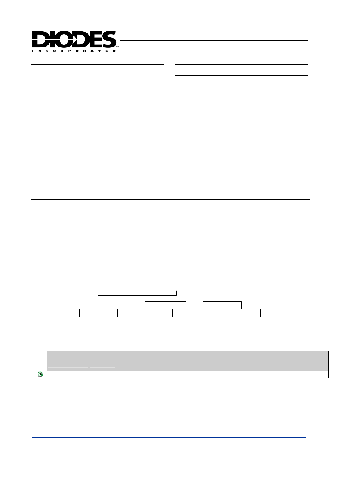
Ordering Information
A P 1 2 1 2 X X X X
Enable
Active -High
:
H
Active -Low
:
L
Package
S:SOP-8L
Lead Free
L : Lead Free
G : Green
Note: 1. RoHS revision 13.2.2003. Glass and High Temperature Solder Exemptions Applied, see EU Directive Annex Notes 5 and 7.
Device
(Note 3)
AP1212XS
Package
Code
Packaging
S SOP-8L 100 -U 2500/Tape & Reel -13
Quantity
Tube 13” Tape and Reel
Part Number
Suffix
Note: 2. Pad layout as shown on Diodes Inc. suggested pad layout document AP02001, which can be on found our website at
http://www.diodes.com/datasheets/ap02001.pdf.
Packing
U
:
-
Tube
-13:Taping
Quantity
Part Number
Suffix
AP1212 Rev. 2 1 of 12 FEBRUARY 2007
www.diodes.com © Diodes Incorporated
Page 2

AP1212
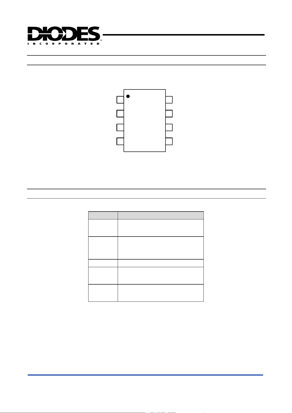
Pin Assignments
EN1
FLG1
FLG2
EN2
1
2
3
4
(Top View)
AP1212
DUAL USB HIGH-SIDE POWER SWITCH
OUT1
8
IN
7
GND
6
5
OUT2
SOP-8L
Pin Descriptions
Name Description
EN1
EN2
FLG1
FLG2
GND Supply return.
IN
OUT1
OUT2
AP1212 Rev. 2 2 of 12 FEBRUARY 2007
Enable: Logic-compatible enable
input. ( H: active high, L: active low).
Do not float.
Fault Flag: Active-low, open-drain
output. Indicates over current,
UVLO, and thermal shutdown.
Supply Input: Output MOSFET drain.
Also supplies IC’s internal circuitry.
Connect to positive supply.
Switch Output: Output MOSFET
source. Typically connect to
switched side of load.
www.diodes.com © Diodes Incorporated
Page 3

AP1212
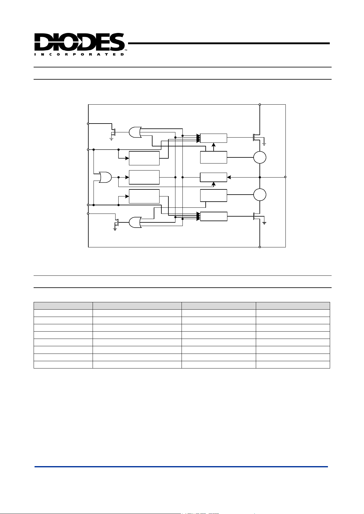
Block Diagram
FLG1
EN1
EN2
FLG2
Charge
Pump
Thermal
Shutdown
Charge
Pump
DUAL USB HIGH-SIDE POWER SWITCH
OUT1
Driver
Current
Limit
UVLO
Current
Limit
Driver
CS
CS
Power N-MOSFET
IN
OUT2
Absolute Maximum Ratings (Note 3)
Symbol Parameter Rating Unit
VIN Supply Voltage +7 V
V
Fault Flag Voltage +7 V
FLG
I
Fault Flag Current 50 mA
FLG
V
Output Voltage +7 V
OUT
VEN Control Input Range –0.3 to V
TST Storage Temperature -65 to +150
ESD HBM Note 3 500 V
ESD MM Note 3 150 V
+2 V
IN
Power N-MOSFET
°C
AP1212 Rev. 2 3 of 12 FEBRUARY 2007
www.diodes.com © Diodes Incorporated
Page 4

O
p
/
/
AP1212
DUAL USB HIGH-SIDE POWER SWITCH
Operating Ratings (Note 4)
Symbol Parameter Rating Unit
VIN Supply Voltage
T
O
P
Θ
Θ
JA
JC
Thermal Resistance SOP Junction to Ambient
Thermal Resistance SOP J unction to Case
erating Junction Temperature -40 to +125
Note: 3. Exceeding the absolute maximum rating may damage the device.
4. The device is not guaranteed to function outside its operating rating.
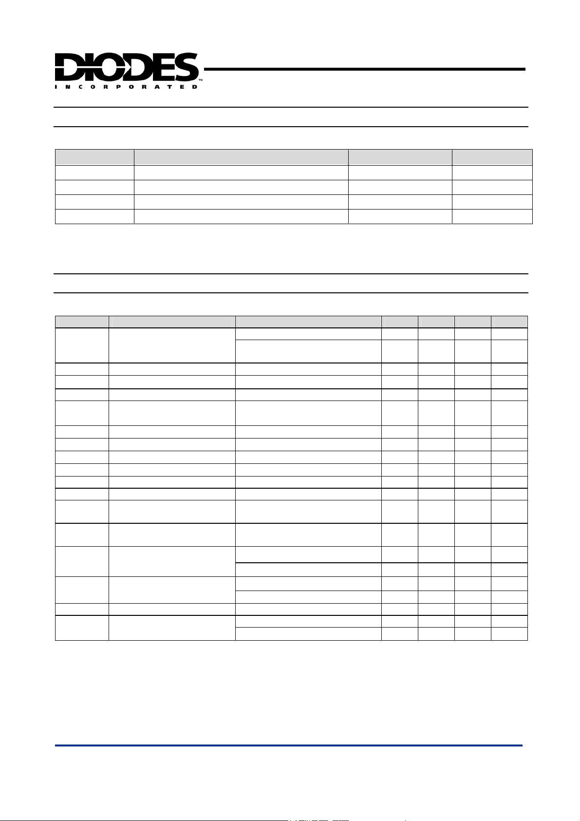
Electrical Characteristics (Under the conditions of V
=+5V and TA =25oC, unless otherwise specified)
IN
Symbol Parameter Conditions Min. Typ. Max. Unit
Switch off, OUT = open (Note 6)
ICC Supply Current
All switches on, OUT = open
(Note 6)
VIT Enable Input Threshold (Note 6) 0.8 1.7 2.40 V
IEN Enable Input Current VEN = 0V to 5.5V -1
CEN Enable Input Capacitance 1 pF
= 2.7V ~ 5.5V, I
V
R
Switch Resistance
DS(ON)
T
Output Turn-On Delay
OND
TR Output Turn-On Ri se Time
T
Output Turnoff Delay
OFFD
TF Output Turnoff Fall Time
I
Output Leakage Current Each output (output disabled) 10 µA
LEAK
I
Continuous Load Current Each output 0.6 A
OUT
IOS Short-circuit Current Limit
I
Current-Limit Threshold
LIM
TTS
RFO
I
FOH
Over-temperature
Shutdown Threshold
Error Flag Output
Resistance
Error Flag Off Current V
UVLO UVLO Threshold
IN
500mA, each switch
R
= 10Ω each output
L
R
= 10Ω each output
L
R
= 10Ω each output
L
R
= 10Ω each output
L
Each output (enable into load),
V
= 0V
OUT
Ramped load applied to
enabled output
TJ increasing 140
T
decreasing 130
J
V
= 5V, IL = 10mA 10 25
IN
V
= 3.3V, IL = 10mA 15 40
IN
= 5V 0.01 1 µA
FLAG
VIN = increasing 2.5 V
V
= decreasing 2.3 V
IN
OUT
=
Note: 5. Devices are ESD sensitive. Handling precautions are recommended. Human Body model, tested per JEDEC 22-A114.
Machine model, tested per JEDEC 22-A115.
6. Off is V
≦0.8V and on is VEN≧2.4V for the AP1212H. Off is VEN≧2.4V and on is VEN≦0.8V for the AP1212L.
EN
AP1212 Rev. 2 4 of 12 FEBRUARY 2007
www.diodes.com © Diodes Incorporated
+2.7 to +5.5 V
°C
165
26
0.50 5 µA
110 160 µA
±0.01
°C
°C
1 µA
110 140
30 µS
1 mS
0.5 10 µS
0.5 10 µS
0.8 1.0 1.25 A
1.0 1.2 1.4 A
W
W
mΩ
°C
°C
Ω
Ω
Page 5

AP1212
Typical Performance Characteristics
On-Resistance vs. Supply Voltage
120
116
112
108
104
100
96
ON-RESISTANCE(ms)
92
88
2.5 3.0 3.5 4.0 4.5 5.0 5.5
SUPPLY VOLTAGE
Turn-On Rise Time vs. Supply Voltage
1.4
1.2
S)
1.0
m
(
0.8
0.6
RISE TIME
0.4
0.2
0.0
2.5 3.0 3.5 4.0 4.5 5.0
O
C
85
SUPPLY VOLTAGE (V)
On-Current vs. Supply Voltage
220
200
180
160
140
120
100
80
CURRENT (≤gA)
60
40
20
0
2.5 3.0 3.5 4.0 4.5 5.0 5.5
-40OC
SUPPLY VOLTAGE (V)
25OC
25
O
C
RL=10ohm
T=25℃
(V)
O
-40
C
RL=10ohm
CL=47 uF
85OC
5.5
DUAL USB HIGH-SIDE POWER SWITCH
On-Resistance vs. Temperature
160
150
140
130
120
110
100
90
ON-RESISTANCE (ms)
80
70
60
-
40-20
=5V
VSUPPLY
2
0
0
TEMPERATURE (
0
4
V
SUPPLY
RL=10ohm
0
6
O
)
C
=3.3V
8010
0
Turn-On Rise Time vs. Temperature
1.4
1.2
)
mS
1.0
(
0.8
0.6
RISE TIME
0.4
0.2
0.0
-40 -20 0 20 40 60 80 100
SUPPLY
V
=5V
V
SUPPLY=3.3V
TEMPERATURE
O
(
C)
RL=10ohm
CL=47uF
On-Current vs. Temperature
200
180
160
140
120
100
80
60
CURRENT (≤gA)
40
20
0
-40-200 20406080100
V
=5V
SUPPLY
=3.3V
V
SUPPLY
TEMPERATURE (OC)
AP1212 Rev. 2 5 of 12 FEBRUARY 2007
www.diodes.com © Diodes Incorporated
Page 6

AP1212
DUAL USB HIGH-SIDE POWER SWITCH
Typical Performance Characteristics (Continued)
Off-Current vs. Supply Voltage
350
300
250
200
150
100
CURRENT (nA)
50
0
-50
2.5 3.0 3.5 4.0 4.5 5.0 5.5
85OC
SUPPLY VOLTAGE (V)
Enable Threshold vs. Supply Voltage
2.0
25OC
-40OC
350
300
250
200
150
100
CURRENT (nA)
-50
2.0
Off-Current vs. Temperature
50
0
-40-200 20406080100
Enable Threshold vs. Temperature
V
=5V
SUPPLY
TEMPERATURE (OC)
V
SUPPLY
=3.3V
1.8
1.6
VEN RISING
1.4
1.2
ENABLE THRESHOLD (V)
1.0
2.5 3.0 3.5 4.0 4.5 5.0 5.5
SUPPLY VOLTAGE (V)
Short-Circuit Current-Limit vs. Supply Voltage
1.6
1.4
1.2
1.0
0.8
0.6
0.4
CURRENT-LIMIT (A)
0.2
0.0
2.5 3.0 3.5 4.0 4.5 5.0 5.5
-40OC
SUPPLY VOLTAGE (V)
VEN FALLING
T=25OC
25OC
85OC
1.8
VEN RISING
1.6
1.4
1.2
ENABLE THRESHOLD (V)
1.0
-40 -20 0 20 40 60 80 100
VEN FALLING
TEMPERATURE (OC)
VIN=5V
Short-Circuit Current-Limit vs. Temperature
1.6
1.4
1.2
1.0
0.8
0.6
0.4
CURRENT-LIMIT (A)
0.2
0.0
-40-200 20406080100
TEMPERATURE (OC)
V
=5V
SUPPLY
V
SUPPLY
=3.3V
AP1212 Rev. 2 6 of 12 FEBRUARY 2007
www.diodes.com © Diodes Incorporated
Page 7

AP1212
DUAL USB HIGH-SIDE POWER SWITCH
Typical Performance Characteristics (Continued)
Current-Limit Threshold vs. Supply Voltage
1.6
1.4
1.2
1.0
0.8
0.6
0.4
0.2
CURRENT-LIMIT THRESHOLD (A)
0.0
2.5 3.0 3.5 4.0 4.5 5.0 5.5
SUPPLY VOLTAGE (V)
UVLO Threshold vs. Temperature
3.0
2.5
2.0
-40OC
25OC
85OC
VIN RISING
VIN FALLING
Current-Limit Threshold vs. Temperature
1.6
1.4
1.2
1.0
0.8
0.6
0.4
CURRENT-LIMIT (A)
0.2
0.0
-40-200 20406080100
V
SUPPLY
V
=3.3V
SUPPLY
TEMPERATURE (OC)
=5V
1.5
1.0
UVLO THRESHOLD (V)
0.5
0.0
-40-200 20406080100
TEMPERATURE (OC)
AP1212 Rev. 2 7 of 12 FEBRUARY 2007
www.diodes.com © Diodes Incorporated
Page 8

A
AP1212
Functional Characteristics
Turn-On/Turn-Off (AP1212H)
VEN
V
FLG
V
OUT
I
OUT
Turn-Off (AP1212H) Enabled Into Short (AP1212H)
Inrush Current
TIME (10mS/div.)
140 m
VIN=5V
CL=47µF
R
=35Ω
L
DUAL USB HIGH-SIDE POWER SWITCH
Turn-On (AP1212H)
Output Turn-On
Rise Time
Inrush Current
TIME (200µS/div.)
VIN=5V
CL=47µF
R
=35Ω
L
140 mA
VEN
VIN=5V
V
FLG
V
I
OUT
OUT
140 mA
CL=47µF
R
=35Ω
L
V
FLG
Short-Circuit Current
TIME (2mS/div.) TIME (500µS/div.)
Current-Limit Response (AP1212H) Current-Limit Response (AP1212H)
VEN
V
OUT
Current-Limit
Threshold
Thermal Shutdown
Short-Circuit Current
VIN=5V
C
=47µF
L
Hysteresis (10OC)
VEN
V
FLG
V
OUT
Current-Limit
Threshold
Short-Circuit Current
TIME (50mS/div.) TIME (20µS/div.)
V
=5V
IN
VIN=5V
C
=47µF
L
AP1212 Rev. 2 8 of 12 FEBRUARY 2007
www.diodes.com © Diodes Incorporated
Page 9

AP1212
Typical Application Circuit
Power
Supply
3.3V 5V
0.1uF
USB
Control
7
2
1
3
4
IN
FLG1
EN1
FLG2
EN2
AP1212
GND
6
DUAL USB HIGH-SIDE POWER SWITCH
Downstream
USB Ports
D+
DVBUS
GND
ferrite bead
D+
DVBUS
GND
ferrite bead
OUT1
OUT2
8
0.1uF
5
ferrite bead
33uF
ferrite bead
33uF0.1uF
Test Circuit
OFF
OFF
ON
ON
EN1
FLG1
FLG2
EN2
10K R1
10K R2
AP1212
OUT1
IN
GND
OUT2
V
CC
+5V
R3>=10
C1
0.1uF
R4>=10
AP1212 Rev. 2 9 of 12 FEBRUARY 2007
www.diodes.com © Diodes Incorporated
Page 10

AP1212
Function Description
Error Flag
An open-drained output of N-channel MOSFET, the FLG
output is pulled low to signal the following fault conditions: input
undervoltage, output current limit, and thermal shutdown.
Current Limit
The current limit threshold is preset internally. It protects
the output MOSFET switches from damage due to undesirable
short circuit conditions or excess inrush current often
encountered during hot plug-in. The low limit of the current limit
threshold of the AP1212 allows a minimum current of 0.5A
through the MOSFET switches. A current limit condition will
signal the error flag.
Thermal Shutdown
When the chip temperature exceeds 140ºC for any reason
other than over current fault of either one of the two MOSFET
switches, the thermal shutdown function turns off both MOSFET
switches and signals the error flag. A hysteresis of 10ºC prevents
the MOSFETs from turning back on until the chip temperature
drops to below 130ºC.
DUAL USB HIGH-SIDE POWER SWITCH
Supply Filtering
A 0.1µF to 1µF bypass capacitor from IN to GND, located
near the device, is strongly recommended to control supply
transients. Without a bypass capacitor, an output short may
cause sufficient ringing on the input (from supply lead inductance)
to damage internal control circuitry.
Transient Droop Requirements
USB applications support dynamic attachment (hot plug-in)
of peripherals. A current surge is caused by the input capacitance
of downstream device. Ferrite beads are recommended in series
with all power and ground connector pins. Ferrite beads reduce
EMI and limit the inrush current during hot-attachment by filtering
high-frequency signals.
Short Circuit Transient
Bulk capacitance provides the short-term transient current
needed during a hot-attachment event. With a 33µF, 16V
tantalum or 100µF, 10V electrolytic capacitor mounted close to
downstream connector per port should provide transient drop
protection.
Printed Circuit Layout
The power circuitry of USB printed circuit boards requires
a customized layout to maximize thermal dissipation and to
minimize voltage drop and EMI.
AP1212 Rev. 2 10 of 12 FEBRUARY 2007
www.diodes.com © Diodes Incorporated
Page 11

AP1212
Marking Information
SOP-8L
Logo
Part Number
Device Package Identification Code
AP1212XS SOP-8L AP1212
(Top View)
8
AP1212 X
DUAL USB HIGH-SIDE POWER SWITCH
5
Enable Type
H : Active High
L : Active Low
L : Lead Free
G : Green
YY WW XX
ID code: internal
Xth week: 01~52
Year: "01" =2001
1 4
SOP-8L
"02" =2002
~
Package Information
Package Type: SOP-8L
7°~9°
1.27typ
4.80/5.30
0.3/0.5
5.79/6.20
3.70/4.10
1.30/1.50
1.75max.
0.08/0.25
0.20typ
Detail "A"
0.35max.
45°
3.70/4.10
0.38/1.27
0.254
7°~9°
Gauge Plane
Seating Plane
Detail "A"
AP1212 Rev. 2 11 of 12 FEBRUARY 2007
www.diodes.com © Diodes Incorporated
Page 12

AP1212
DUAL USB HIGH-SIDE POWER SWITCH
IMPORTANT NOTICE
Diodes Incorporated and its subsidiaries reserve the right to make modifications, enhancements, improvements, corrections or other changes without further
notice to any product herein. Diodes Incorporated does not assume any liability arising out of the application or use of any product described herein; neither
does it convey any license under its patent rights, nor the rights of others. The user of products in such applications shall assume all risks of such use and will
agree to hold Diodes Incorporated and all the companies whose products are represented on our website, harmless against all damages.
LIFE SUPPORT
Diodes Incorporated products are not authorized for use as critical components in life support devices or systems without the expressed written approval of the
President of Diodes Incorporated.
AP1212 Rev. 2 12 of 12 FEBRUARY 2007
www.diodes.com © Diodes Incorporated
 Loading...