

Page 1
Dual MOSFET Driver
GND PGND
SD
IN
DRVLSD
SRMON
OVPSET
DLY
VCC
VCCGD
BST
DRVH
SW
DRVL
ADP3410
TO PWM
CONTROLLER
5V
V
BATT
V
OUT
V
CC
V
CC
CONTROL
AND
OVERLAP
PROTECTION
CIRCUIT
ADP3410
4.4V
1.2V
VCC
VCCGD
GND
SD
IN
DLY
OVPSET
DRVLSD
PGND
BST
DRVH
SW
DRVL
SRMON
a
FEATURES
All-In-One Synchronous Buck Driver
One PWM Signal Generates Both Drives
Anticross-Conduction Protection Circuitry
Programmable Transition Delay
Synchronous Override Control
Undervoltage Lockout
Programmable Overvoltage Shutdown
V
Good Signal Drives Auxiliary Circuits
CC
Shutdown Quiescent Current < 10 A
APPLICATIONS
Mobile Computing CPU Core Power Converters
Multiphase Desktop CPU Supplies
Single-Supply Synchronous Buck Converters
Standard-to-Synchronous Converter Adaptations
with Bootstrapping
ADP3410
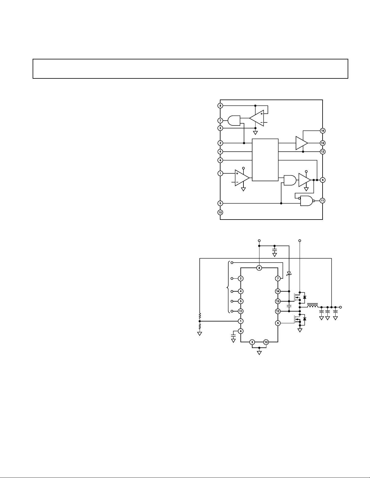
FUNCTIONAL BLOCK DIAGRAM
GENERAL DESCRIPTION
The ADP3410 is a dual MOSFET driver optimized for driving
two N-channel FETs that are the two switches in the nonisolated synchronous buck power converter topology. Each of
the drivers is capable of driving a 3000␣ pF load with a 20␣ ns
propagation delay and a 30␣ ns transition time. One of the drivers
can be bootstrapped, and is designed to handle the high-voltage
slew rate associated with “floating” high-side gate drivers. The
ADP3410 has several protection features: overlapping drive
prevention (ODP), undervoltage lockout (UVLO) with performance specified at very low VCC levels, and overvoltage protection
(OVP) that can be used to monitor either the input or output.
Additional features include: programmable transition delay, a
synchronous drive override control pin, a synchronous drive
status monitor and, in conjunction with exiting from the UVLO
mode, a V
Good (VCCGD) signal capable of driving a 10␣ mA
CC
load. The quiescent current, when the device is disabled, is less
than 10 µA.
REV. 0
Information furnished by Analog Devices is believed to be accurate and
reliable. However, no responsibility is assumed by Analog Devices for its
use, nor for any infringements of patents or other rights of third parties
which may result from its use. No license is granted by implication or
otherwise under any patent or patent rights of Analog Devices.
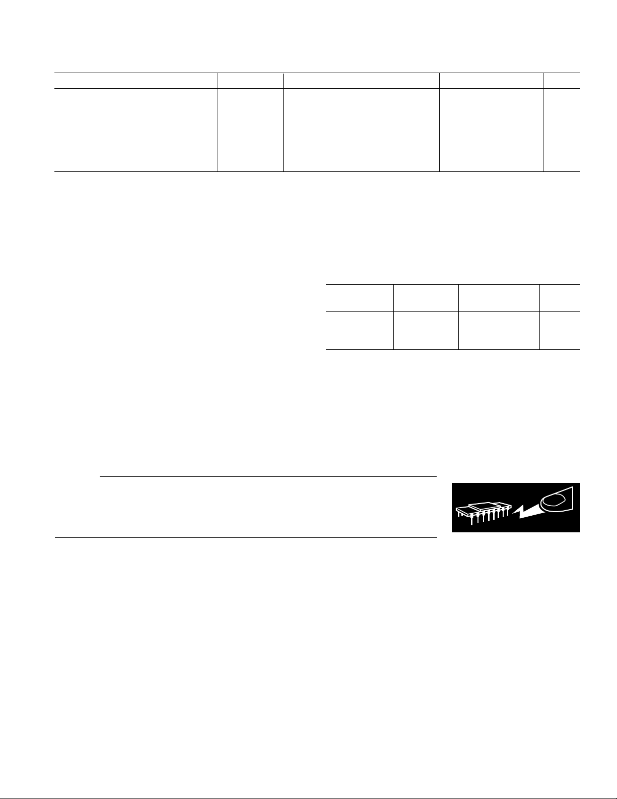
Figure 1. Typical Application Circuit
One Technology Way, P.O. Box 9106, Norwood, MA 02062-9106, U.S.A.
Tel: 781/329-4700 World Wide Web Site: http://www.analog.com
Fax: 781/326-8703 © Analog Devices, Inc., 1999
Page 2

(TA = 0ⴗC to 85ⴗC, VCC = 5 V, VBST = 4 V to 26 V, SD > 2 V, unless otherwise
1
ADP3410–SPECIFICATIONS
noted)
Parameter Symbol Conditions Min Typ Max Unit
SUPPLY
Supply Voltage Range V
Quiescent Current I
CC
CCQ
Shutdown Mode V
< 0.8 V 10 µA
SD
4.15 5.0 6.0 V
Operating Mode VSD > 2.0 V, No Switching 1 2 mA
VCCGD OUTPUT
Output Voltage High V
Output Voltage Low V
VCCGD Propagation Delay
(See Figure 4) tpdl
2, 3
tpdh
, SD Goes High 10 µs
VCCGD
VCCGD
= 4.6 V, I
CC
< UVLO, I
CC
= 10 mA 4.5 4.55 V
LOAD
= 10 µA 0.1 0.2 V
LOAD
SD Goes Low 10 µs
SYNCHRONOUS RECTIFIER
MONITOR
Output Voltage High 4.15 V
Output Voltage Low V
Transition Time
Propagation Delay
2
2, 3
tr
SRMON, tfSRMONVCC
tpdh
SRMON
= 4.6 V, C
CC
= 4.6 V, C
= 100 pF 50 mV
LOAD
= 100 pF 20 ns
LOAD
DRVLSD Is High and 15 ns
DRVL Goes High, or
DRVLSD Goes Low
tpdl
SRMON
DRVLSD Is High and 15 ns
DRVL Goes Low
UNDERVOLTAGE LOCKOUT
UVLO Threshold 4.2 4.4 4.6 V
UVLO Hysteresis 0.05 V
UVLO Logic Active Threshold 1.5 V
2, 3
UVLO
Propagation Delay tpdh
(See Figure 5) tpdl
UVLO
UVLO
V
Goes High 10 µs
CC
V
Goes Low 10 µs
CC
OVERVOLTAGE PROTECTION
Trip Threshold 1.145 1.2 1.255 V
Hysteresis 0.8 V
Bias Current 0.2 1.0 µA
2, 3, 4
OVP
Propagation Delay tpdh
OVP
V
= 4.6 V, OVPSET Goes High 0.5 µs
CC
SYNCHRONOUS RECTIFIER ENABLE
DRVLSD
Input Voltage High
Input Voltage Low
Propagation Delay
(See Figure 3) tpdh
SD INPUT
Input Voltage High
Input Voltage Low
PWM INPUT (IN)
Input Voltage High
Input Voltage Low
5
2, 3
5
5
5
2.0 V
0.8 V
tpdl
5
,VCC = 4.6 V, 30 ns
DRVLSD
DRVLSD
C
LOAD (DRVL)
= 3 nF
2.0 V
0.8 V
5
2.0 V
0.8 V
THERMAL SHUTDOWN
Overtemperature Trip Point 165 °C
OTP Hysteresis 10 °C
HIGH-SIDE DRIVER
Output Resistance, Sourcing Current V
Output Resistance, Sinking Current V
DRVH Transition Times
(See Figure 6) tf
DRVH Propagation Delay
(See Figure 6) tpdl
2
2, 3
tr
,V
DRVH
DRVH
tpdh
,V
DRVH
DRVH
– V
BST
BST
BST
BST
= 4.6 V 2.5 5 Ω
SW
– V
= 4.6 V 2.5 5 Ω
SW
– V
= 4.6 V, C
SW
= 3 nF 20 35 ns
LOAD
– VSW = 4.6 V 10 20 Note 6 ns
25 ns
REV. 0–2–
Page 3
ADP3410
Parameter Symbol Conditions Min Typ Max Unit
LOW-SIDE DRIVER
Output Resistance, Sourcing Current V
Output Resistance, Sinking Current V
DRVL Transition Times
(See Figure 6) tf
DRVL Propagation Delay
(See Figure 6) tpdl
NOTES
1
All limits at temperature extremes are guaranteed via correlation using standard Statistical Quality Control (SQC) methods.
2
AC specifications are guaranteed by characterization, but not production tested.
3
For propagation delays, tpdh refers to the specified signal going high, tpdl refers to it going low.
4
Propagation delay measured until DRVL begins its transition.
5
Logic inputs meet typical CMOS I/O conditions for source/sink current (~1 mA).
6
Maximum propagation delay = 40 ns max + (1 ns/pF × C
Specifications subject to change without notice.
2
2, 3
tr
DRVL,
DRVL
tpdh
DLY
DRVL
DRVL
).
= 4.6 V 2.5 5 Ω
CC
= 4.6 V 2.5 5 Ω
CC
VCC = 4.6 V, C
= 3 nF 20 35 ns
LOAD
VCC = 4.6 V 5 30 ns
25 ns
ABSOLUTE MAXIMUM RATINGS*
ORDERING GUIDE
VCC to PGND . . . . . . . . . . . . . . . . . . . . . . . . –0.3 V to +7 V
BST to PGND . . . . . . . . . . . . . . . . . . . . . . . . –0.3 V to +30 V
BST to SW . . . . . . . . . . . . . . . . . . . . . . . . . . . –0.3 V to +7 V
SW to PGND . . . . . . . . . . . . . . . . . . . . . . . . –2.0 V to +25 V
Model Temperature Package Package
Range Description Option
ADP3410KRU 0°C to 85°C Thin Shrink Small RU-14
OVPSET to PGND . . . . . . . . . . . . . . . . . . . . –0.3 V to +10 V
SD, IN, DRVLSD to GND . . . . . . . . . . . . . . –0.3 V to +7.3 V
GND to PGND . . . . . . . . . . . . . . . . . . . . . . . . . . . . . . ±0.3 V
Operating Ambient Temperature Range . . . . . . . 0°C to 85°C
Operating Junction Temperature Range . . . . . . 0°C to 125°C
. . . . . . . . . . . . . . . . . . . . . . . . . . . . . . . . . . . . 155°C/W
θ
JA
. . . . . . . . . . . . . . . . . . . . . . . . . . . . . . . . . . . . . 40°C/W
θ
JC
Storage Temperature Range . . . . . . . . . . . . –65°C to +150°C
Lead Temperature (Soldering, 10 sec) . . . . . . . . . . . . . 300°C
*This is a stress rating only; operation beyond these limits can cause the device to
be permanently damaged.
CAUTION
ESD (electrostatic discharge) sensitive device. Electrostatic charges as high as 4000 V readily
accumulate on the human body and test equipment and can discharge without detection.
Although the ADP3410 features proprietary ESD protection circuitry, permanent damage may
occur on devices subjected to high-energy electrostatic discharges. Therefore, proper ESD
precautions are recommended to avoid performance degradation or loss of functionality.
Outline Package
(TSSOP-14)
WARNING!
ESD SENSITIVE DEVICE
REV. 0 –3–
Page 4
ADP3410
PIN FUNCTION DESCRIPTIONS
Pin Mnemonic Function
1 OVPSET Overvoltage Shutdown Sense Input. Shutdown occurs when this pin is driven above the specified thresh-
old. It is a high-impedance comparator input, so an external resistor divider can be used to scale the
controlling voltage for OVP.
2 SD Shutdown. When high, this pin enables normal operation. When low, VCCGD, DRVH, and DRVL are
forced low and the supply current (ICC
3 GND Signal Ground. The input signal and the capacitor at DLY should be closely referenced to this ground.
4 IN TTL-level input signal which has primary control of the drive outputs.
5 DRVLSD Synchronous Rectifier Enable. When low, this signal forces DRVL low. The propagation delay time is on
the order of that for the main input signal, so it can be used for real time modulation control of DRVL.
When DRVLSD is high, DRVL is enabled and controlled by IN.
6 DLY Low-High-Transition Delay. A capacitor from this pin to ground programs the propagation delay
from turn-off of the lower FET to turn-on of the upper FET. The formula for the low-high-transition
delay is DLY = C
× (1␣ ns/pF) + 20␣ ns. The rise time for turn-on of the upper FET is not included in
DLY
the formula.
7 VCCGD V
Good. This pin indicates the status of the undervoltage lockout. When VCC is high enough for the
CC
device to exit UVLO mode, the VCCGD pin is pulled up to V
signal is capable of acting as a switched power rail for external circuitry, since it can source 10␣ mA and
sink 10 µA.
8 VCC Input Supply. This pin should be bypassed to PGND with ~1 µF ceramic capacitor.
9 DRVL Synchronous Rectifier Drive. Output drive for the lower (synchronous rectifier) FET.
10 PGND Power Ground. Should be closely connected to the source of the lower FET.
11 SRMON Synchronous Rectifier Monitor. When DRVLSD is high, SRMON follows DRVL. When DRVLSD is
low, SRMON is high. TTL-type output.
12 SW This pin is connected to the buck switching node, close to the upper FET’s source. It is the floating return
for the upper FET drive signal. Also, it is used to monitor the switched voltage to prevent turn-on of the
lower FET until the voltage is below ~1 V. Thus, the high-low-transition delay is determined at this pin
according to operating conditions. This pin can be subjected to voltages as low as 2 V below PGND.
13 DRVH Buck Drive. Output drive for the upper (buck) FET.
14 BST Floating Bootstrap Supply for the upper FET. A capacitor connected between BST and SW pins holds
this bootstrapped voltage for the high-side FET as it is switched. The capacitor should be chosen between
0.1 µF and 1 µF.
) is minimized as specified.
Q
with the specified low impedance. This
CC
PIN CONFIGURATION
OVPSET
SD
GND
DRVLSD
DLY
VCCGD
IN
1
2
3
4
5
6
7
ADP3410
14
13
12
11
10
9
8
–4–
BST
DRVH
SW
SRMON
PGND
DRVL
VCC
REV. 0
Page 5

ADP3410
5V
VCC
SD
V
CC
VCCGD
DLY
C
DLY
DRVL
10%
V
IN
Ra
V
OUT
OVPSET
Rb
CC
1V
BIAS
ENABLE
UVLO
DELAY
1.2V
D1
ADP3410
VCC
4.4V
BST
DRVH
SW
VCC
DRVL
C
BST
PGND
V
BATT
Q1
Q2
DRVLSD
DRVL
DRVLSD
GND
SRMON
Figure 2. Functional Block Diagram
IN
2.0V
0.8V
tpdl
Figure 3.
DRVLSD
DRVLSD
Propagation Delay
tpdh
DRVLSD
REV. 0
–5–
Page 6

ADP3410
SD
VCCGD
V
VCCGD
2V
0.8V
tpdh
VCCGD
3.5V
tpdI
VCCGD
10% V
CC
Figure 4. VCCGD Propagation Delay
CC
tpdh
UVLO THRESHOLD UVLO THRESHOLD–HYSTERESIS
tpdI
UVLO
10% V
CC
UVLO
90% V
CC
Figure 5. UVLO Propagation Delay
DRVL
DRVH-SW
SW
IN
DRVL
90%
tf
DRVL
10%
tpdh
DRVH
10%
tr
DRVH
10%
10%
DRVL
tr
DRVL
90%
tpdl
DRVH
tf
DRVH
90%
V
TH
90%
V
TH
tpdh
1V
tpdl
Figure 6. Nonoverlap Timing Diagram
–6–
REV. 0
Page 7

JUNCTION TEMPERATURE – 8C
30
25
0
0
8525
TIME – ns
50 75
20
15
10
5
RISE TIME
FALL TIME
V
CC
= 5V
C
LOAD
= 3nF
CAPACITANCE – nF
35
0
TIME – ns
30
25
20
15
10
5
0
123456
V
CC
= 5V
T
A
= 258C
DRVH
DRVL
Typical Performance Characteristics–ADP3410
2V/DIV
DRVH
DRVL
VOLTAGE
IN
VCC = 5V
= 3nF
C
LOAD
= 0V
20ns/DIV
TIME – ns
V
SW
Figure 7. DRVH Fall and DRVL Rise
Times
35
= 5V
V
CC
= 3nF
C
LOAD
30
25
20
15
TIME – ns
10
5
RISE TIME
FALL TIME
2V/DIV
DRVL
DRVH
VOLTAGE
IN
VCC = 5V
= 3nF
C
LOAD
= 20pF
20ns/DIV
TIME – ns
C
DLY
Figure 8. DRVL Fall and DRVH Rise
Times
40
= 5V
V
CC
= 258C
T
A
30
20
TIME – ns
10
DRVH
DRVL
Figure 9. DRVH Rise and Fall Times
vs. Temperature
0
0
AMBIENT TEMPERATURE – 8C
50 75
Figure 10. DRVL Rise and Fall Times
vs. Temperature
30
VCC = 5V
= 3nF
C
LOAD
25
20
15
TIME – ns
10
5
0
0
Figure 13. Propagation Delay vs.
Temperature
tpdl
DRVH
tpdl
DRVL
25
50 75
JUNCTION TEMPERATURE – 8C
REV. 0
100 125
8525
0
0
2345
CAPACITANCE – nF
Figure 11. DRVH and DRVL Rise
Times vs. Load Capacitance
40
VCC = 5V
= 258C
T
35
A
= 3nF
C
LOAD
30
25
20
15
10
SUPPLY CURRENT – mA
5
0
0
IN FREQUENCY – kHz
Figure 14. Supply Current vs.
Frequency
61
Figure 12. DRVH and DRVL Fall Times
vs. Load Capacitance
11.0
V
= 5V
CC
= 250kHz
f
IN
= 3nF
C
LOAD
10.5
10.0
9.5
SUPPLY CURRENT – mA
9.0
1200200 400 600 800 1000
0 12525
50 75 100
JUNCTION TEMPERATURE – 8C
Figure 15. Supply Current vs.
Temperature
–7–
Page 8

ADP3410
THEORY OF OPERATION
The ADP3410 is a dual MOSFET driver optimized for driving
two N-channel FETs in a synchronous buck converter topology.
A single PWM input signal is all that is required to properly
drive the high-side and the low-side FETs. Each driver is
capable of driving a 3 nF load with only a 20 ns transition time.
A more detailed description of the ADP3410 and its features
follows. Refer to the functional block diagram.
Low-Side Driver
The low-side driver is designed to drive low-R
DS(ON)
N-channel
MOSFETs. The maximum output resistance for the driver is
5 Ωs for both sourcing and sinking gate current. The low-output
resistance allows the driver to have 20 ns rise and fall times into
a 3 nF load. The bias to the low-side driver is internally connected to the VCC supply and PGND.
When the driver is enabled, the driver’s output is 180° out of
phase with the PWM input. When the driver is shut down or the
entire ADP3410 is in shutdown or in under voltage lockout, the
low-side gate is held low.
High-Side Driver
The high-side driver is designed to drive a floating low R
DS(ON)
N-channel MOSFET. The maximum output resistance for the
driver is 5 Ωs for both sourcing and sinking gate current. The
low output resistance allows the driver to have 20 ns rise and fall
times into a 3 nF load. The bias voltage for the high-side driver
is developed by an external bootstrap supply circuit, which is
connected between the BST and SW pins.
The bootstrap circuit comprises a Schottky diode, D1, and
bootstrap capacitor, C
. When the ADP3410 is starting up,
BST
the SW pin is at ground, so the bootstrap capacitor will charge
up to VCC
through D1. As the input voltage ramps up and
exceeds the UVLO threshold, the high-side driver is enabled.
When the PWM input goes high, the high-side driver will begin
to turn the high-side FET, Q1, ON by pulling charge out of
. As Q1 turns ON, the SW pin will rise up to V
C
BST
forcing the BST pin to V
BATT
+ V
, which is enough gate-
C(BST)
BATT
,
to-source voltage to hold Q1 ON. To complete the cycle, Q1 is
switched OFF by pulling the gate down to the voltage at the
SW pin. When the low-side FET, Q2, turns ON, the SW pin is
pulled to ground. This allows the bootstrap capacitor to charge
up to VCC
again.
The high-side driver’s output is in phase with the PWM input.
When the driver is in under-voltage lockout, the high-side gate
is held low.
Overlap Protection Circuit
The Overlap Protection Circuit (OPC) prevents both of the
main power switches, Q1 and Q2, from being ON at the same
time. This is done to prevent shoot-through currents from
flowing through both power switches and the associated losses
that can occur during their ON-OFF transitions. The overlap
protection circuit accomplishes this by adaptively controlling the
delay from Q1’s turn OFF to Q2’s turn ON, and by programming the delay from Q2’s turn OFF to Q1’s turn ON.
To prevent the overlap of the gate drives during Q1’s turn OFF
and Q2’s turn ON, the overlap circuit monitors the voltage at
the SW pin. When the PWM input signal goes low, Q1 will
begin to turn OFF (after a propagation delay), but before Q2
can turn ON, the overlap protection circuit waits for the voltage
at the SW pin to fall from V
to 1 V. Once the voltage on the
BATT
SW pin has fallen to 1 V, Q2 will begin turn ON. By waiting for
the voltage on the SW pin to reach 1 V, the overlap protection
circuit ensures that Q1 is OFF before Q2 turns on, regardless of
variations in temperature, supply voltage, gate charge, and drive
current.
To prevent the overlap of the gate drives during Q2’s turn OFF
and Q1’s turn ON, the overlap circuit provides a programmable
delay that is set by a capacitor on the DLY pin. When the PWM
input signal goes high, Q2 will begin to turn OFF (after a propagation delay), but before Q1 can turn ON, the overlap protection
circuit waits for the voltage at DRVL to drop to around 10% of
VCC. Once the voltage at DRVL has reached the 10% point,
the overlap protection circuit will wait for a 20 ns typical propagation delay plus an additional delay based on the external
capacitor, C
. The delay capacitor adds an additional 1 ns/pF
DLY
of delay. Once the programmable delay period has expired, Q1
will begin turn ON. The delay allows time for current to commutate from the body diode of Q2 to an external Schottky
diode, which allows turn-off losses to be reduced. Although not
as foolproof as the adaptive delay, the programmable delay adds
a safety margin to account for variations in size, gate charge, and
internal delay of the external power MOSFETs.
Overvoltage Protection
An overvoltage protection circuit monitors the output voltage
for an overvoltage condition. This condition is possible if Q1
should fail. If this should occur, the output voltage would begin
to rise up to the battery voltage where it would pose the threat
of damage to the devices connected to the output. By adding a
resistor divider, Ra and Rb, to the OVPSET pin, the output
voltage can be monitored for this fault condition.
If the voltage on the OVPSET pin exceeds the 1.2 V threshold,
this indicates a fault condition and Q1 is turned OFF and the
low-side FET (synchronous rectifier) is turned ON. The power
switches will remain in this state until the voltage on the
OVPSET pin falls below 400 mV. The turn-on of Q2 is not
delayed by monitoring the SW voltage, but the triggering of
OVP is intentionally slow to avoid false triggering.
Low-Side Driver Enable
The low-side driver enable (DRVLSD) allows external control
of the synchronous rectifier. This is particularly useful for maintaining efficiency under light load conditions. At light loads, the
PWM duty cycle becomes small, meaning the high-side switch is
ON for a very short time and the synchronous rectifier is ON for
the remainder of the period. Under these conditions, the inductor current ramps up during the short high-side switch ON time,
and then ramps down during the synchronous rectifier’s ON
time. If the inductor current reaches zero and there is still time
left in the period, the inductor current will begin to go negative.
Negative current indicates that current is being drawn out of the
output capacitor through the inductor and low-side FET to
ground, incurring extra losses in the process. If the DRVLSD is
used to shut down the low-side driver when the inductor
current reaches zero, the light load efficiency can be dramatically
improved. If inductor current information is not available, but
a microprocessor is performing a power management function,
it can shut down the synchronous rectifier when in a sleep or
stand-by mode.
When the DRVLSD input is low, the low-side driver output
goes low. When the DRVLSD input is high the low-side driver
is enabled and controlled by the PWM input. The propagation
–8–
REV. 0
Page 9

ADP3410
delay from the DRVLSD input to the DRVL output is about
30 ns.
Synchronous Rectifier Monitor
The synchronous rectifier monitor provides a TTL output signal
for use by the PWM controller. The SRMON output follows the
DRVL signal when the low-side driver is enabled and goes high
when the low-side driver is shut down.
Shutdown
The shutdown input is used for power management. If the circuits running off of the buck converter are not needed, the
ADP3410 can be shut down to conserve power.
When the SD pin is high, the ADP3410 is enabled for normal
operation. Pulling the SD pin low forces the VCCGD, DRVH
and DRVL outputs low turning the buck converter OFF and
reducing the VCC
Undervoltage Lockout
supply current to less than 10 µA.
The undervoltage lockout (UVLO) circuit holds both FET
driver outputs low during VCC
supply ramp up. The UVLO
logic becomes active and in control of the driver outputs at a
supply voltage of 1.5 V. The UVLO circuit will wait until the
supply has reached a voltage high enough to bias logic
VCC
level FETs fully ON, around 4.4 V, before releasing control
of the drivers to the PWM input.
VCC Good
The power ready signal, VCCGD, indicates the status of the
supply. When the device is in UVLO, the VCCGD output
VCC
is pulled low by an NMOS transistor. Upon exiting UVLO mode,
the VCCGD pin is pulled up to VCC
with a 5 Ω PMOS transis-
tor capable of sourcing current to external load circuits. As can
be seen from the block diagram, the UVLO comparator output
and the SD signal are ANDed together to become the VCCGD
output, so when the device is put into shutdown the VCCGD
output will be low regardless of the VCC voltage.
Thermal Shutdown
The thermal shutdown circuit protects the ADP3410 against
damage due to excessive power dissipation. Under extreme
conditions, high ambient temperature and high-power dissipation,
the die temperature can rise up to the over-temperature trip
point of 165°C. If the die temperature exceeds 165°C, the
thermal shutdown circuit will turn the output drivers OFF. The
drivers will remain disabled until the junction temperature has
decreased by 10°C, at which point the drivers are enabled again.
APPLICATION INFORMATION
Supply Capacitor Selection
For the supply input (VCC) of the ADP3410, a local bypass
capacitor is recommended to reduce the noise and to supply
some of the peak currents drawn. Use a 5 µF to 10 µF, low ESR
capacitor. Multilayer ceramic chip (MLCC) capacitors provide
the best combination of low ESR and small size and can be
obtained from the following vendors:
Murata GRM235Y5V106Z16 http://www.murata.com
Taiyo-Yuden EMK325F106ZF http://www.t-yuden.com
Tokin C23Y5V1C106ZP http://www.tokin.com
A lower cost alternative may be to use a 5 µF to 10 µF tantalum
capacitor with a small (1 µF) ceramic in parallel. Keep the
ceramic capacitor as close as possible to the ADP3410.
Bootstrap Circuit
The bootstrap circuit requires a charge storage capacitor, C
BST
,
and a Schottky diode, D1, as shown in Figure 2. Selecting these
components can be done after the high-side FET has been chosen.
The bootstrap capacitor must have a voltage rating that is able
to handle the maximum battery voltage plus 5 V. A minimum
50 V rating is recommended. The capacitance is determined
using the following equation:
Q
C
BST
where Q
is the voltage droop allowed on the high-side FET drive.
∆V
BST
GATE
=
∆
V
BST
is the total gate charge of the high-side FET, and
GATE
(1)
For example, the IRF7811 has a total gate charge of about
20 nC. For an allowed droop of 200 mV, the required bootstrap
capacitance is 100 nF. Look for a good quality ceramic capacitor.
A Schottky diode is recommended for the bootstrap diode due
to its low forward drop, which maximizes the drive available for
the high-side FET. The bootstrap diode must have a minimum
40 V rating to withstand the maximum battery voltage plus 5 V.
The average forward current can be estimated by:
where f
IQf
MAX
≈×
F AVG
()
GATE MAX
(2)
is the maximum switching frequency of the controller.
The peak surge current rating should be checked in circuit since
this is dependent on the source impedance of the 5 V supply,
and the ESR of C
Setting the OVP Threshold
BST
.
The ADP3410 can shut down the high-side FET drive when the
OVPSET input exceeds the threshold voltage. The voltage at
which V
trips the overvoltage protection is set by selecting
OUT
the values for Ra and Rb shown in Figure 2. The threshold for
the OVP is calculated using:
VV
=×+
12 1.
OVP
where V
is the desired OVP threshold voltage at V
OVP
Ra
Rb
OUT
(3)
.
In order to minimize the bias current error, Rb should be less
than or equal to 24 kΩ. By selecting a value for Rb ≤ 24 kΩ and
solving for Ra gives the following formula:
V
Ra
OVP
=−
121.
×
Rb
V
(4)
Note that the minimum the OVP threshold can be is 1.2 V when
Ra is zero.
Delay Capacitor Selection
The delay capacitor, C
, is used to add an additional delay
DLY
when the low-side FET drive turns off and when the high-side
drive starts to turn on. The delay capacitor adds 1 ns/pF of
additional time to the 20 ns of fixed delay.
If a delay capacitor is required, a good quality ceramic capacitor
with an NPO or COG dielectric or a good quality mica capacitor
should be used. Both types of capacitors are available in the
1 pF to 100 pF range and have excellent temperature and
leakage characteristics.
REV. 0
–9–
Page 10

ADP3410
Printed Circuit Board Layout Considerations
Use the following general guidelines when designing printed
circuit boards:
1. Trace out the high-current paths and use short, wide traces
to make these connections.
2. Split the ground connections. Use separate planes for the
signal and power grounds, and tie them together at a single
point near the ADP3410.
3. The VCC
possible to VCC
Q2
2N3906
Q1
MJD210
C20
10mF
bypass capacitor should be located as close as
and PGND pins.
3.3V
R10
10k
FROM
CPU
VRON
V
100nF
C2
C3
68mF
C14
100
mF
R1
51.1kV
R2
160kV
1
2
3
4
5
6
7
8
9
10
11
12
13
14
ADP3421
VHYS
CLSET
LTO
LTI
LTB
VID4
VID3
VID2
VID1
VID0
CLKDRV
CLKFB
IODRV
IOFB
U1
RAMP
DACOUT
CORE
UVLO
PWRGD
CS–
CS+
REG
VCC
OUT
GND
SSC
SSL
R16
C31
C22
1nF
R11
220k
3.3k
1pF
R21, 10k
C41
1pF
C21
1.5nF
R12
V
470
28
27
26
25
C1
24
100nF
23
22
21
20
19
18
17
16
SD
15
V
C29
100pF
kV
C25
R15
V
332
22nF
R19
kV
V
2
R17
75k
V
R18
kV
576
C23
1nF
R6
7.5
R5
kV
10
kV
Figure 16. Typical Application Circuit
Typical Application Circuit
The circuit in Figure 16 shows how the ADP3410 can be combined with the ADP3421 to form a total power conversion solution
for a microprocessor. The combination provides the supply
voltages for the core processor, the I/O interface, and the clock.
100
R22
kV
C18
10pF
U2
ADP3410
1
OVPSET
2
SD
3
GND
4
IN
5
DRVLSD
6
DLY
7
VCCGD VCC
BST
DRVH
SW
SRMON
PGND
DRVL
14
13
12
11
10
9
8
C28
10mF
5V
D2
10BQ040
C17
100nF
M2
IRF7811
R8
2.2
V
C10
10
mF
M1
IRF7811
IRF7811
C15
10mF
M3
R9
2.2
V
VIN
C16
10mF
C32
15nF
L1
R
mH
1
D1
10BQ040
VCC ON CORE SENSE
CS
5m
C4–C6,
C11, C12,
C26, C27
220mF 3 7
VCC CPU IO
VCC CPU CLK
V
V GATE
R20
10
CORE
V
VCC
CPU
GND
–10–
REV. 0
Page 11

OUTLINE DIMENSIONS
Dimensions shown in inches and (mm).
14-Lead Thin Shrink Small Outline Package (TSSOP)
(RU-14)
0.201 (5.10)
0.193 (4.90)
ADP3410
PIN 1
0.006 (0.15)
0.002 (0.05)
SEATING
PLANE
14
0.0256
(0.65)
BSC
8
71
0.0433 (1.10)
MAX
0.0118 (0.30)
0.0075 (0.19)
0.177 (4.50)
0.169 (4.30)
0.256 (6.50)
0.246 (6.25)
0.0079 (0.20)
0.0035 (0.090)
C3698–8–10/99
88
08
0.028 (0.70)
0.020 (0.50)
REV. 0
PRINTED IN U.S.A.
–11–
 Loading...