

Datasheet 74LCX244WMX, 74LCX244WM, 74LCX244SJX, 74LCX244SJ, 74LCX244MTCX Datasheet (Fairchild Semiconductor)
...Page 1
February 1994
Revised April 1999
74LCX244 Low Voltage Buffer/Line Driver with 5V Tolerant Inputs and Outputs
© 1999 Fairchild Semiconductor Corporation DS500107.prf www.fairchildsemi.com
74LCX244
Low Voltage Buffer/Line Driver with 5V Tolerant
Inputs and Outputs
General Description
The LCX244 con tains eight non-inverting buffers with 3STATE outputs. The device may be employed as a memory address driver, clock driver and bus-oriented transm itter/receiver. The LCX244 is designed for low voltage (2.5V
or 3.3V) V
CC
applications with capability of interfacing to a
5V signal environment.
The LCX244 is fabrica ted with an advanced CMOS tech-
nology to achieve high spee d operation while mai ntaining
CMOS low power dissipation.
Features
■ 5V tolerant inputs and outputs
■ 2.3V–3.6V V
CC
specifications provided
■ 6.5 ns t
PD
max (VCC = 3.3V), 10 µA ICC max
■ Power down high impedance inputs and outputs
■ Supports live insertion/withdrawal (Note 1)
■ ±24 mA output drive (V
CC
= 3.0V)
■ Implements patented noise/EMI reduction circuitry
■ Latch-up performance exceeds 500 mA
■ ESD performance:
Human body model > 2000V
Machine model > 200V
Note 1: To ensure the high-impedan c e state during power up or down, OE
should be tied to VCC through a pull-up res istor: the m inimu m value or t he
resistor is determin ed by the current-sourcing capability of the driver.
Ordering Code:
Devices also availab le in Tape and Reel. Specify by appending th e s uffix let t er “X” to the ordering cod e.
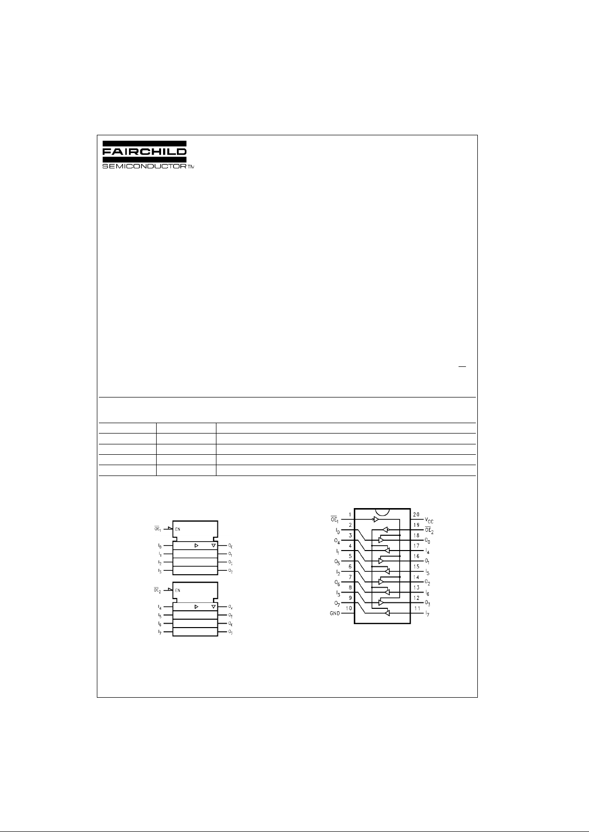
Logic Symbol
IEEE/IEC
Connection Diagram
Order Number Package Number Package Description
74LCX244WM M20B 20-Lead Small Outline Integrated Circuit (SOIC), JEDEC MS-013, 0.300” Wide
74LCX244SJ M20D 20-Lead Small Outline Package (SOP), EIAJ TYPE II, 4.4mm Wide
74LCX244MSA MSA20 20-Lead Shrink Small Outline Package (SSOP), EIAJ TYPE II, 5.3mm Wide
74LCX244MTC MTC20 20-Lead Thin Shrink Small Outline Package (TSSOP), JEDEC MO-153, 4.4mm Wide
Page 2
www.fairchildsemi.com 2
74LCX244
Pin Descriptions
Truth Tables
H = HIGH Voltage Level
L = LOW Voltage Level
X = Immaterial
Z = High Impedance
Pin Names Description
OE
1
, OE
2
3-STATE Output Enable Inputs
I
0–I7
Inputs
O
0–O7
Outputs
Inputs Outputs
OE
1
I
n
(Pins 12, 14, 16, 18)
LL L
LH H
HX Z
Inputs Outputs
OE
2
I
n
(Pins 3, 5, 7, 9)
LL L
LH H
HX Z
Page 3
3 www.fairchildsemi.com
74LCX244
Absolute Maximum Ratings(Note 2)
Recommended Operating Conditions (Note 4)
Note 2: The Absolute Maximum Ratings are those values beyond which the safety of the device cannot be guaranteed. The device should not be operated
at these limits. The parametric values defined in the Electrical Characteristics tables are not guaranteed at the Absolute Maximum Ratings. The “Recommended Operating C onditions” table will def ine the conditions for ac t ual device operation.
Note 3: I
O
Absolute Maximum Rating must be observed.
Note 4: Unused inputs or I/Os must be held HIGH or LOW. They may not float.
DC Electrical Characteristics
Symbol Parameter Value Conditions Units
V
CC
Supply Voltage −0.5 to +7.0 V
V
I
DC Input Voltage −0.5 to +7.0 V
V
O
DC Output Voltage −0.5 to +7.0 Output in 3-STATE
V
−0.5 to V
CC
+ 0.5 Output in HIGH or LOW State (Note 3)
I
IK
DC Input Diode Current −50 VI < GND mA
I
OK
DC Output Diode Current −50 VO < GND
mA
+50 V
O
> V
CC
I
O
DC Output Source/Sink Current ±50 mA
I
CC
DC Supply Current per Supply Pin ±100 mA
I
GND
DC Ground Current per Ground Pin ±100 mA
T
STG
Storage Temperature −65 to +150 °C
Symbol Parameter Min Max Units
V
CC
Supply Voltage Operating 2.0 3.6
V
Data Retention 1.5 3.6
V
I
Input Voltage 0 5.5 V
V
O
Output Voltage HIGH or LOW State 0 V
CC
V
3-STATE 0 5.5
I
OH/IOL
Output Current VCC = 3.0V–3.6V ±24
mAV
CC
= 2.7V–3.0V ±12
V
CC
= 2.3V–2.7V ±8
T
A
Free-Air Operating Temperature −40 85 °C
∆t/∆V Input Edge Rate, V
IN
= 0.8V–2.0V, VCC = 3.0V 0 10 ns/V
Symbol Parameter Conditions
V
CC
TA = −40°C to +85°C
Units
(V) Min Max
V
IH
HIGH Level Input Voltage 2.3 − 2.7 1.7
V
2.7 − 3.6 2.0
V
IL
LOW Level Input Voltage 2.3 − 2.7 0.7
V
2.7 − 3.6 0.8
V
OH
HIGH Level Output Voltage IOH = −100 µA2.3 − 3.6 VCC − 0.2
V
IOH = −8 mA 2.3 1.8
IOH = −12 mA 2.7 2.2
IOH = −18 mA 3.0 2.4
IOH = −24 mA 3.0 2.2
V
OL
LOW Level Output Voltage IOL = 100 µA2.3 − 3.6 0.2
V
IOL = 8 mA 2.3 0.6
IOL = 12 mA 2.7 0.4
IOL = 16 mA 3.0 0.4
IOL = 24 mA 3.0 0.55
I
I
Input Leakage Current 0 ≤ VI ≤ 5.5V 2.3 − 3.6 ±5.0 µA
I
OZ
3-STATE Output Leakage 0 ≤ VO ≤ 5.5V 2.3 − 3.6 ±5.0
µA
VI = VIH or V
IL
I
OFF
Power-Off Leakage Current VI or VO = 5.5V 0 10 µA
Page 4

www.fairchildsemi.com 4
74LCX244
DC Electrical Characteristics (Continued)
Note 5: Outputs dis abled or 3-STATE only.
AC Electrical Characteristics
Note 6: Skew is defined as t he absolute value of t he difference between the actual pro pagation delay for a ny t w o separate outpu ts of the same device . T he
specification applies to any outputs swit c hing in the same direc ti on, eit her HIGH-to-LOW (t
OSHL
) or LOW-to-HIGH (t
OSLH
).
Dynamic Switching Characteristics
Capacitance
Symbol Parameter Conditions
V
CC
TA = −40°C to +85°C
Units
(V) Min Max
I
CC
Quiescent Supply Current VI = VCC or GND 2.3 − 3.6 10
µA
3.6V ≤ VI, VO ≤ 5.5V (Note 5) 2.3 − 3.6 ±10
∆I
CC
Increase in ICC per Input VIH = VCC −0.6V 2.3 − 3.6 500 µA
Symbol Parameter
TA = −40°C to +85°C, RL = 500Ω
Units
VCC = 3.3V ± 0.3V VCC = 2.7V VCC = 2.5V ± 0.2
CL= 50 pF CL = 50 pF CL = 30 pF
Min Max Min Max Min Max
t
PHL
Propagation Delay 1.5 6.5 1.5 7.5 1.5 7.8
ns
t
PLH
Data to Output 1.5 6.5 1.5 7.5 1.5 7.8
t
PZL
Output Enable Time 1.5 8.0 1.5 9.0 1.5 10.0
ns
t
PZH
1.5 8.0 1.5 9.0 1.5 10.0
t
PLZ
Output Disable Time 1.5 7.0 1.5 8.0 1.5 8.4
ns
t
PHZ
1.5 7.0 1.5 8.0 1.5 8.4
t
OSHL
Output to Output Skew
(Note 6)
1.0
ns
t
OSLH
1.0
Symbol Parameter Conditions
V
CC
(V)
TA = 25°C
Units
Typical
V
OLP
Quiet Output Dynamic Peak V
OL
CL = 50 pF, VIH = 3.3V, VIL = 0V 3.3 0.8
V
CL = 30 pF, VIH = 2.5V, VIL = 0V 2.5 0.6
V
OLV
Quiet Output Dynamic Valley V
OL
CL = 50 pF, VIH = 3.3V, VIL = 0V 3.3 −0.8
V
CL = 30 pF, VIH = 2.5V, VIL = 0V 2.5 −0.6
Symbol Parameter Conditions Typical Units
C
IN
Input Capacitance VCC = Open, VI = 0V or V
CC
7pF
C
OUT
Output Capacitance VCC = 3.3V, VI = 0V or V
CC
8pF
C
PD
Power Dissipation Capacitance VCC = 3.3V, VI = 0V or VCC, f = 10 MHz 25 pF
Page 5

5 www.fairchildsemi.com
74LCX244
AC LOADING and WAVEFORMS Generic for LCX Family
FIGURE 1. AC Test Circuit (C
L
includes probe and jig capacitance)
Waveform for Inverting and Non-Inverting Functions
Propagation Delay. Pulse Width and t
rec
Waveforms
3-STATE Output Low Enable and
Disable Times for Logic
3-STATE Output High Enable and
Disable Times for Logic
Setup Time, Hold Time and Recovery Time for Logic
t
rise
and t
fall
FIGURE 2. Waveforms
(Input Characteristics; f =1MHz, t
R
= tF = 3ns)
Test Switch
t
PLH
, t
PHL
Open
t
PZL
, t
PLZ
6V at VCC = 3.3 ± 0.3V
V
CC
x 2 at VCC = 2.5 ± 0.2V
t
PZH,tPHZ
GND
Symbol
V
CC
3.3V ± 0.3V 2.7V 2.5V ± 0.2V
V
mi
1.5V 1.5V VCC/2
V
mo
1.5V 1.5V VCC/2
V
x
VOL + 0.3V VOL + 0.3V VOL + 0.15V
V
y
VOH − 0.3V VOH − 0.3V VOH − 0.15V
Page 6

www.fairchildsemi.com 6
74LCX244
Schematic Diagram Generic for LCX Family
FIGURE 3.
Page 7

7 www.fairchildsemi.com
74LCX244
Physical Dimensions inches (millimeters) unless otherwise noted
20-Lead Small Outline Integrated Circuit (SOIC), JEDEC MS-013, 0.300” Wide
Package Number M20B
20-Lead Small Outline Package (SOP), EIAJ TYPE II, 4.4mm Wide
Package Number M20D
Page 8

www.fairchildsemi.com 8
74LCX244
Physical Dimensions inches (millimeters) unless otherwise noted (Continued)
20-Lead Shrink Small Outline Package (SSOP), EIAJ TYPE II, 5.3mm Wide
Package Number MSA20
Page 9

Fairchild does not assume any responsibility for use of any circuitry described, no circuit patent licenses are implied and Fairchild reserves the right at any time without notice to change said circuitry and specifications.
74LCX244 Low Voltage Buffer/Line Driver with 5V Tolerant Inputs and Outputs
LIFE SUPPORT POLICY
FAIRCHILD’S PRODUCTS ARE NOT AUTHORIZED FOR USE AS CRITICAL COMPONENTS IN LIFE SUPPORT
DEVICES OR SYSTEMS WITHOUT THE EXPRESS WRITTEN APPROVAL OF THE PRESIDENT OF FAIRCHILD
SEMICONDUCTOR CORPORATION. As used herein:
1. Life support devices or systems are dev ic es or syste ms
which, (a) are intended for surgical implant into the
body, or (b) support or sustain life, and (c) whose failure
to perform when properly used in accordance with
instructions for use provided i n the labe li ng, can be re asonably expected to result in a significant injury to the
user.
2. A critical componen t in any com ponent o f a l ife supp ort
device or system whose failu re to perform can b e reasonably expected to c ause th e fa i lure of the li fe s upp or t
device or system, or to affect its safety or effectiveness.
www.fairchildsemi.com
Physical Dimensions inches (millimeters) unless otherwise noted (Continued)
20-Lead Thin Shrink Small Outline Package (TSSOP), JEDEC MO-153, 4.4mm Wide
Package Number MTC20
 Loading...