

Page 1
© 1999 Fairchild Semiconductor Corporation DS009504 www.fairchildsemi.com
April 1988
Revised August 1999
74F251A 8-Input Multiplexer with 3-STATE Outputs
74F251A
8-Input Multiplexer with 3-STATE Outputs
General Description
The 74F251A is a hig h-speed 8-i nput digital m ultiplexer. It
provides, in one package, the ability to select one bit of
data from up to eight sources. It can be used as a universal
function generator t o generate any logic function of four
variables. Both assertion and negation outputs are provided.
Features
■ Multifunctional capability
■ On-chip select logic decoding
■ Inverting and non-inverting 3-STATE outputs
Ordering Code:
Devices also availab le in Tape and Reel. Specify by appending th e s uffix let t er “X” to the ordering code.
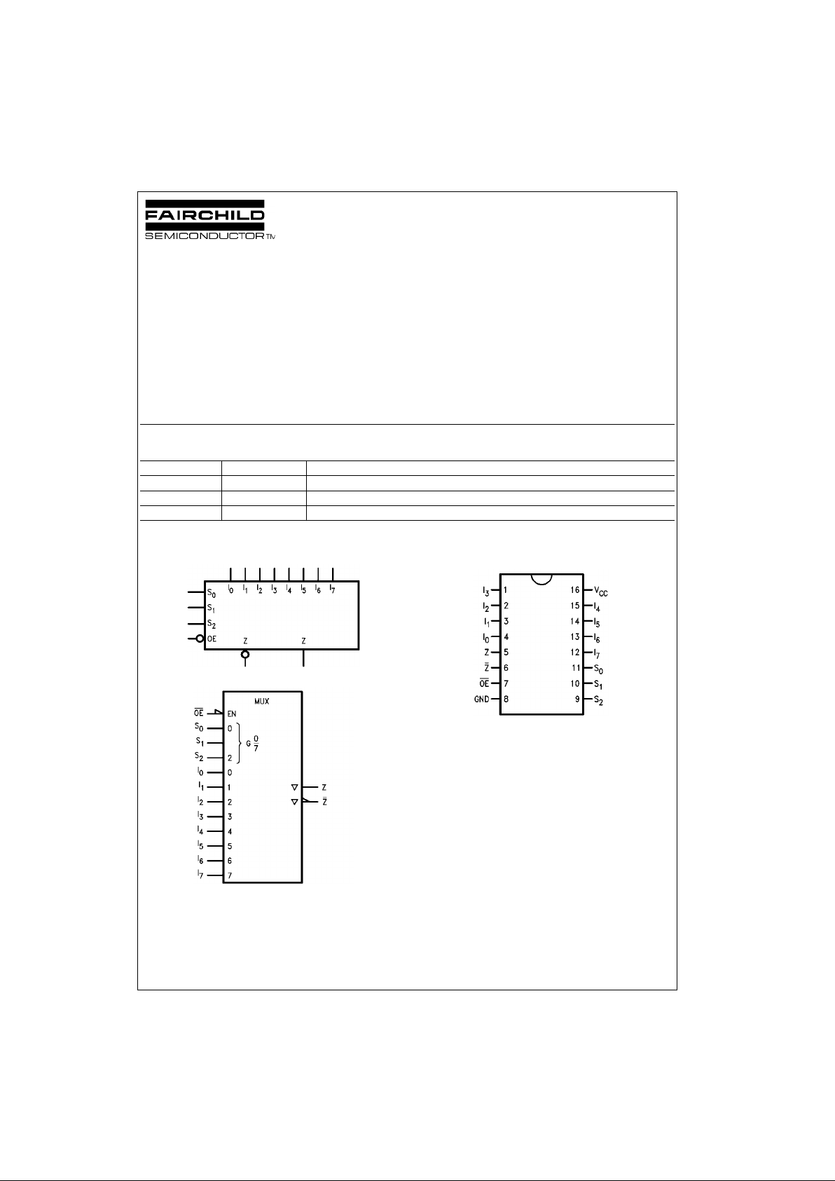
Logic Symbols
IEEE/IEC
Connection Diagram
Order Number Package Number Package Description
74F251ASC M16A 16-Lead Small Outline Integrated Circuit (SOIC), JEDEC MS-012, 0.150 Narrow
74F251ASJ M16D 16-Lead Small Outline Package (SOP), EIAJ TYPE II, 5.3mm Wide
74F251APC N16E 16-Lead Plastic Dual-In-Line Package (PDIP), JEDEC MS-001, 0.300 Wide
Page 2
www.fairchildsemi.com 2
74F251A
Unit Loading/Fan Out
Functional Description
This device is a logical implementa tion of a single-pole, 8position switch with the switch position controlled by the
state of three Selec t inputs, S
0
, S1, S2. Both assertion and
negation outputs are provided. The Output Enable input
(OE
) is active LOW. When it is activated, the logic functi on
provided at the output is:
Z = OE
•(I0•S0•S1 •S2 + I1•S0•S 1•S2 +
I
2•S0•S1•S2
+ I3•S0•S1•S2 +
I
4•S0•S1•S2
+ I5•S0•S1•S2 +
I
6•S0•S1•S2
+ I7•S0•S1•S2)
When the Output Enabl e is HIGH, both outpu ts are in the
high impedance (High Z) state. This feature allows multiplexer expansion by tyin g the ou tput s of up to 128 dev ices
together. When the outputs of the 3-STATE devices are
tied together, all but one device must b e i n th e h igh im ped ance state to avo id high currents that would exc eed the
maximum ratings. The Output Enable signals should be
designed to ensure there is no over lap in the active L OW
portion of the enable voltages.
Tr uth Table
H = HIGH Voltage Level
L = LOW Voltage Level
X = Immaterial
Z = High Impedance
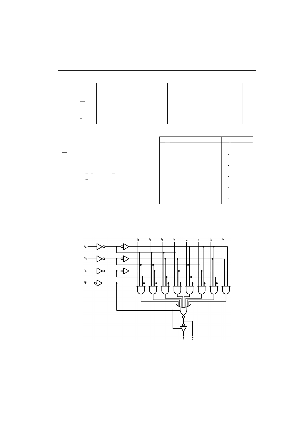
Logic Diagram
Please note that this diagram is provided o nly f or t he understanding of lo gic operations and should not be used to estimate propagation delays.
Pin Names Description
U.L.
Input I
IH/IIL
HIGH/LOW
Output I
OH/IOL
S0–S2Select Inputs 1.0/1.0 20 µA/−0.6 mA
OE
3-STATE Output Enable Input (Active LOW) 1.0/1.0 20 µA/−0.6 mA
I
0–I7
Multiplexer Inputs 1.0/1.0 20 µA/−0.6 mA
Z 3-STATE Multiplexer Output 150/40 (33.3) −3 mA/24 mA (20 mA)
Z
Complementary 3-STATE Multiplexer Output 150/40 (33.3) −3 mA/24 mA (20 mA)
Inputs Outputs
OE
S
2
S
1
S
0
Z Z
HXXXZZ
LLLLI
0
I
0
LLLHI1I
1
LLHLI2I
2
LLHHI3I
3
LHLLI4I
4
LHLHI5I
5
LHHLI6I
6
LHHHI7I
7
Page 3

3 www.fairchildsemi.com
74F251A
Absolute Maximum Ratings(Note 1) Recommended Operating
Conditions
Note 1: Absolute maximum ratings are values beyon d which the device
may be damaged or have its useful life impaired . Functional operation
under these condit ions is not implied.
Note 2: Either voltage limit or curren t limit is sufficient to protect in puts.
DC Electrical Characteristics
Storage Temperature −65°C to +150°C
Ambient Temperature under Bias −55°C to +125°C
Junction Temperature under Bias −55°C to +150°C
V
CC
Pin Potential to Ground Pin −0.5V to +7.0V
Input Voltage (Note 2) −0.5V to +7.0V
Input Current (Note 2) −30 mA to +5.0 mA
Voltage Applied to Output
in HIGH State (with V
CC
= 0V)
Standard Output −0.5V to V
CC
3-STATE Output −0.5V to +5.5V
Current Applied to Output
in LOW State (Max) twice the rated I
OL
(mA)
Free Air Ambi ent Temperature 0°C to +70°C
Supply Voltage +4.5V to +5.5V
Symbol Parameter Min Typ Max Units
V
CC
Conditions
V
IH
Input HIGH Voltage 2.0 V Recognized as a HIGH Signal
V
IL
Input LOW Voltage 0.8 V Recognized as a LOW Signal
V
CD
Input Clamp Diode Voltage −1.2 V Min IIN = −18 mA
V
OH
Output HIGH 10% V
CC
2.5
VMin
IOH = −1 mA
Voltage 10% V
CC
2.4 IOH = −3 mA
5% V
CC
2.7 IOH = −1 mA
5% V
CC
2.7 IOH = −3 mA
V
OL
Output LOW 10% V
CC
0.5 V Min IOL = 24 mA
Voltage
I
IH
Input HIGH
5.0 µAMaxVIN = 2.7V
Current
I
BVI
Input HIGH Current
7.0 µAMaxVIN = 7.0V
Breakdown Test
I
CEX
Output HIGH
50 µAMaxV
OUT
= V
CC
Leakage Current
V
ID
Input Leakage
4.75 V 0.0
IID = 1.9 µA
Test All Other Pins Grounded
I
OD
Output Leakage
3.75 µA0.0
V
IOD
= 150 mV
Circuit Current All Other Pins Grounded
I
IL
Input LOW Current −0.6 mA Max VIN = 0.5V
I
OZH
Output Leakage Current 50 µAMaxV
OUT
= 2.7V
I
OZL
Output Leakage Current −50 µAMaxV
OUT
= 0.5V
I
OS
Output Short-Circuit Current −60 −150 mA Max V
OUT
= 0V
I
ZZ
Bus Drainage Test 500 µA0.0VV
OUT
= 5.25V
I
CCL
Power Supply Current 15 22 mA Max VO = LOW
I
CCZ
Power Supply Current 16 24 mA Max VO = HIGH Z
Page 4

www.fairchildsemi.com 4
74F251A
AC Electrical Characteristics
Symbol Parameter
TA = +25°CT
A
= −55°C to +125°CTA = 0°C to +70°C
Units
VCC = +5.0V VCC = 5.0V VCC = 5.0V
CL = 50 pF CL = 50 pF CL = 50 pF
Min Typ Max Min Max Min Max
t
PLH
Propagation Delay 3.5 6.0 9.0 3.5 11.5 3.5 9.5
ns
t
PHL
Sn to Z
3.25.07.53.28.03.27.5
t
PLH
Propagation Delay 4.5 7.5 10.5 3.5 14.0 4.5 12.5
ns
t
PHL
Sn to Z 4.0 6.0 8.5 3.0 10.5 4.0 9.0
t
PLH
Propagation Delay 3.0 5.0 6.5 2.5 8.0 3.0 7.0
ns
t
PHL
In to Z
1.52.54.01.56.01.55.0
t
PLH
Propagation Delay 3.5 5.0 7.0 2.5 9.0 2.5 8.0
ns
t
PHL
In to Z 3.5 5.5 7.0 3.5 9.0 3.5 7.5
t
PZH
Output Enable Time 2.5 4.3 6.0 2.0 7.0 2.5 7.0
ns
t
PZL
OE to Z
2.54.36.02.57.52.56.5
t
PHZ
Output Disable Time 2.5 4.0 5.5 2.5 6.0 2.5 6.0
t
PLZ
OE to Z
1.53.04.51.55.01.54.5
t
PZH
Output Enable Time 3.5 5.0 7.0 3.0 8.5 3.0 7.5
ns
t
PZL
OE to Z
3.55.57.53.59.03.58.0
t
PHZ
Output Disable Time 2.0 3.8 5.5 2.0 5.5 2.0 5.5
t
PLZ
OE to Z
1.53.04.51.55.51.54.5
Page 5

5 www.fairchildsemi.com
74F251A
Physical Dimensions inches (millimeters) unless otherwise noted
16-Lead Small Outline Integrated Circuit (SOIC), JEDEC MS-012, 0.150 Narrow
Package Number M16A
16-Lead Small Outline Package (SOP), EIAJ TYPE II, 5.3mm Wide
Package Number M16D
Page 6

www.fairchildsemi.com 6
74F251A 8-Input Multiplexer with 3-STATE Outputs
Physical Dimensions inches (millimeters) unless otherwise noted (Continued)
16-Lead Plastic Dual-In-Line Package (PDIP), JEDEC MS-001, 0.300 Wide
Package Number N16E
Fairchild does not assume any responsibility for use of any circuitry described, no circuit pate nt licenses are implied and
Fairchild reserves the right at any time without notice to change said circuitry and specifications.
LIFE SUPPORT POLICY
FAIRCHILD’S PRODUCTS ARE NOT AUTHORIZED FOR USE AS CRITICAL COMPONENTS IN LIFE SUPPORT
DEVICES OR SYSTEMS WITHOUT THE EXPRESS WRITTEN APPROVAL OF THE PRESIDENT OF FAIRCHILD
SEMICONDUCTOR CORPORATION. As used herein:
1. Life support devices or systems are devices or syste ms
which, (a) are intended for surgical implant into the
body, or (b) support or sustain life, and (c) whose failure
to perform when properly used in accordance with
instructions for use provided in the labeling, can be reasonably expected to result in a significant inju ry to the
user.
2. A critical component i n any compon ent of a lif e support
device or system whose failu re to perform can be reasonably expected to ca use the fa i lure of the life su pp ort
device or system, or to affect its safety or effectiveness.
www.fairchildsemi.com
 Loading...