

Page 1

54ABT543
Octal Registered Transceiver with TRI-STATE
®
Outputs
General Description
The ’ABT543 octal transceiver contains two sets of D-type
latches for temporary storage of data flowing in either direction. Separate Latch Enable and Output Enable inputs are
provided for each register to permit independent control of
inputting and outputting in either direction of data flow.
Features
n Back-to-back registers for storage
n Bidirectional data path
n A and B outputs have current sourcing capability of 24
mA and current sinking capability of 48 mA
n Separate controls for data flow in each direction
n Guaranteed latchup protection
n High impedance glitch free bus loading during entire
power up and power down cycle
n Nondestructive hot insertion capability
n Standard Military Drawing (SMD) 5962-9231401
Ordering Code:
Military Package Package Description
Number
54ABT543J-QML J24A 24-Lead Ceramic Dual-In-Line
54ABT543W-QML W24C 24-Lead Cerpack
54ABT543E-QML E28A 28-Lead Ceramic Leadless Chip Carrier, Type C
Connection Diagrams
TRI-STATE®is a registered trademark of National Semiconductor Corporation.
Pin Assignment for
DIP and Flatpak
DS100218-1
Pin Assignment
for LCC
DS100218-2
August 1998
54ABT543 Octal Registered Transceiver with TRI-STATE Outputs
© 1998 National Semiconductor Corporation DS100218 www.national.com
Page 2

Pin Descriptions
Pin Names Description
OEAB , OEBA
Output Enable Inputs
LEAB , LEBA
Latch Enable Inputs
CEAB , CEBA
Chip Enable Inputs
A
0–A7
Side A Inputs or
TRI-STATE Outputs
B
0–B7
Side B Inputs or
TRI-STATE Outputs
Functional Description
The ’ABT543 contains two sets of D-type latches, with separate input and output controls for each. For data flow from A
to B, for example, the Ato B Enable (CEAB ) input must be
low in order to enter data from the A port or take data from
the B port as indicated in the Data I/O Control Table. With
CEAB low, a low signal on (LEAB ) input makes the A to B
latches transparent; a subsequent low to high transition of
the LEAB line puts the A latches in the storage mode and
their outputs no longer change with the A inputs. With CEAB
and OEAB both low, the B output buffers are active and reflect the data present on the output of the A latches. Control
of data flow from B toAis similar, but using the CEBA , LEBA
and OEBA .
Data I/O Control Table
Inputs Latch Status Output
Buffers
CEAB
LEAB OEAB
H X X Latched High Z
X H X Latched —
L L X Transparent —
X X H — High Z
L X L — Driving
H=High Voltage Level
L=Low Voltage Level
X=Immaterial
Logic Diagram
DS100218-3
www.national.com 2
Page 3

Absolute Maximum Ratings (Note 1)
If Military/Aerospace specified devices are required,
please contact the National SemiconductorSales Office/
Distributors for availability and specifications.
Storage Temperature −65˚C to +150˚C
Ambient Temperature under Bias −55˚C to +125˚C
Junction Temperature under Bias
Ceramic −55˚C to +175˚C
V
CC
Pin Potential to
Ground Pin −0.5V to +7.0V
Input Voltage (Note 2) −0.5V to +7.0V
Input Current (Note 2) −30 mA to +5.0 mA
Voltage Applied to Any Output
in the Disable or Power-Off State −0.5V to +5.5V
in the HIGH State −0.5V to V
CC
Current Applied to Output
in LOW State (Max) twice the rated I
OL
(mA)
DC Latchup Source Current −500 mA
Over Voltage Latchup (I/O) 10V
Recommended Operating
Conditions
Free Air Ambient Temperature
Military −55˚C to +125˚C
Supply Voltage
Military +4.5V to +5.5V
Minimum Input Edge Rate (∆V/∆t)
Data Input 50 mV/ns
Enable Input 20 mV/ns
Clock Input 100 mV/ns
DC Electrical Characteristics
Symbol Parameter ABT543 Units V
CC
Conditions
Min Typ Max
V
IH
Input HIGH Voltage 2.0 V Recognized HIGH Signal
V
IL
Input LOW Voltage 0.8 V Recognized LOW Signal
V
CD
Input Clamp Diode Voltage −1.2 V Min I
IN
=
−18 mA (Non I/O Pins)
V
OH
Output HIGH Voltage 54ABT 2.5 I
OH
=
−3 mA, (A
n,Bn
)
54ABT 2.0 V Min I
OH
=
−24 mA, (A
n,Bn
)
V
OL
Output LOW Voltage 54ABT 0.55 V Min I
OL
=
48 mA, (A
n,Bn
)
V
ID
Input Leakage Test 4.75 V 0.0 I
ID
=
1.9 µA, (Non-I/O Pins)
All Other Pins Grounded
I
IH
Input HIGH Current
5 µA Max
V
IN
=
2.7V (Non-I/O Pins)
(Note 3)
V
IN
=
V
CC
(Non-I/O Pins)
I
BVI
Input HIGH Current Breakdown Test 7 µA Max V
IN
=
7.0V (Non-I/O Pins)
I
BVIT
Input HIGH Current 100 µA Max V
IN
=
5.5V (A
n,Bn
)
Breakdown Test (I/O)
I
IL
Input LOW Current
−5 µA Max
V
IN
=
0.5V (Non-I/O
Pins)(Note 3)
V
IN
=
0.0V (Non-I/O Pins)
I
IH+IOZH
Output Leakage Current 50 µA 0V–5.5V V
OUT
=
2.7V (A
n,Bn
);
OEAB or CEAB=2V
IIL+I
OZL
Output Leakage Current −50 µA 0V–5.5V V
OUT
=
0.5V (A
n,Bn
);
OEAB or CEAB=2V
I
OS
Output Short-Circuit Current −100 −275 mA Max V
OUT
=
0V (A
n,Bn
)
I
CEX
Output HIGH Leakage Current 50 µA Max V
OUT
=
V
CC(An,Bn
)
I
ZZ
Bus Drainage Test 100 µA 0.0V V
OUT
=
5.5V (A
n,Bn
);
All Others GND
I
CCLH
Power Supply Current 50 µA Max All Outputs HIGH
I
CCL
Power Supply Current 30 mA Max All Outputs LOW
I
CCZ
Power Supply Current 50 µA Max Outputs TRI-STATE
All Others at V
CC
or GND
I
CCT
Additional ICC/Input 2.5 mA Max V
I
=
V
CC
− 2.1V
All Others at V
CC
or GND
I
CCD
Dynamic I
CC
No Load Outputs Open, CEAB
3 www.national.com
Page 4
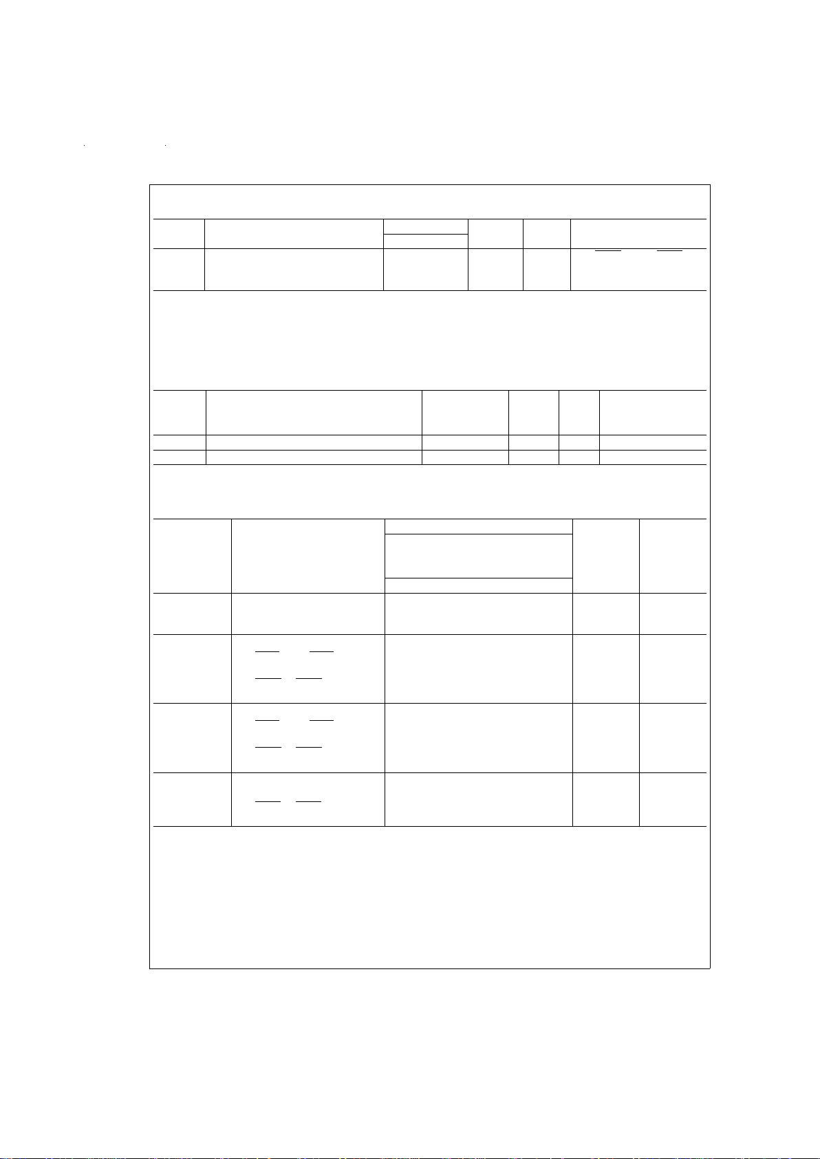
DC Electrical Characteristics (Continued)
Symbol Parameter ABT543 Units V
CC
Conditions
Min Typ Max
(Note 3) 0.18 mA/MHz Max and OEAB=GND,CEBA
=
VCC, One Bit Toggling,
50%Duty Cycle, (Note 4)
Note 1: Absolute maximum ratings are values beyond which the device may be damaged or have its useful life impaired. Functional operation under these conditions
is not implied.
Note 2: Either voltage limit or current limit is sufficient to protect inputs.
Note 3: Guaranteed but not tested.
Note 4: For 8-bit toggling. I
CCD
<
1.4 mA/MHz.
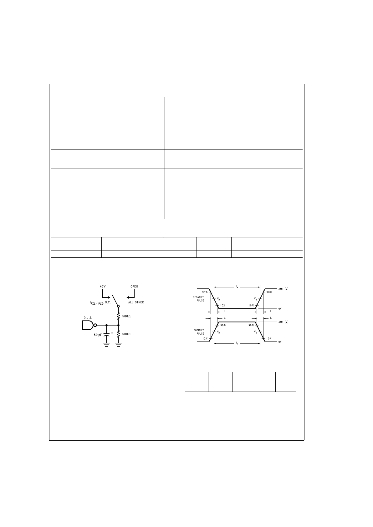
DC Electrical Characteristics
Conditions
Symbol Parameter Min Max Units V
CC
C
L
=
50 pF,
R
L
=
500Ω
V
OLP
Quiet Output Maximum Dynamic V
OL
1.1 V 5.0 T
A
=
25˚C (Note 5)
V
OLV
Quiet Output Minimum Dynamic V
OL
-0.45 V 5.0 T
A
=
25˚C(Note 5)
Note 5: Max number of outputs defined as (n).n−1data inputs are driven 0V to 3V. One output at LOW.
AC Electrical Characteristics
54ABT
T
A
=
−55˚C to +125˚C Fig.
Symbol Parameter V
CC
=
4.5V–5.5V Units No.
C
L
=
50 pF
Min Max
t
PLH
Propagation Delay 1.6 6.4
ns
Figure
4
t
PHL
Anto Bnor Bnto A
n
1.6 6.2
t
PLH
Propagation Delay
t
PHL
LEAB to Bn, LEBA to A
n
1.6 6.6
ns
Figure
4
OEBA or OEAB to Anor
B
n
1.6 6.4
t
PZH
Enable Time
t
PZL
LEAB to Bn, LEBA to A
n
1.3 6.4
ns
Figure
6
OEBA or OEAB to Anor
B
n
1.8 7.4
t
PHZ
Disable Time 2.0 7.2
ns
Figure
6
t
PLZ
CEBA or CEAB to Anor
B
n
1.5 7.0
www.national.com 4
Page 5
AC Operating Requirements
54ABT
T
A
=
−55˚C to +125˚C Fig.
Symbol Parameter V
CC
=
4.5V–5.5V Units No.
C
L
=
50 pF
Min Max
t
S
(H) Setup Time, HIGH or LOW 3.5
ns
Figure
7
tS(L) Anor Bnto LEBA or LEAB 3.0
t
H
(H) Hold Time, HIGH or LOW 2.0
ns
Figure
7
tH(L) Anor Bnto LEBA or LEAB 2.0
t
S
(H) Setup Time, HIGH or LOW 3.3
ns
Figure
7
tS(L) Anor Bnto CEAB or CEBA 2.5
t
H
(H) Hold Time, HIGH or LOW 2.0
ns
Figure
7
tH(L) Anor Bnto CEAB or CEBA 2.0
t
W
(L) Pulse Width, LOW 3.5 ns
Figure
5
Capacitance
Symbol Parameter Typ Units Conditions: T
A
=
25˚C
C
IN
Input Capacitance 5.0 pF V
CC
=
0V (non I/O pins)
C
I/O
(Note 6) Output Capacitance 11.0 pF V
CC
=
5.0V (A
n,Bn
)
Note 6: C
I/O
is measured at frequency, f=1 MHz, PER MIL-STD-883, METHOD 3012.
AC Loading
DS100218-4
*Includes jig and probe capacitance
FIGURE 1. Standard AC Test Load
DS100218-6
FIGURE 2. V
M
=
1.5V
Input Pulse Requirements
Ampli-
tude
Rep.
Rate
t
w
t
r
t
f
3V 1 MHz 500 ns 2.5 ns 2.5 ns
FIGURE 3. Test Input Signal Requirements
5 www.national.com
Page 6
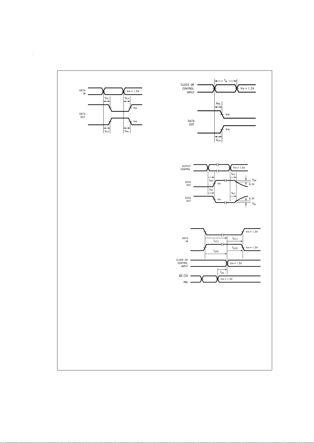
AC Loading (Continued)
DS100218-8
FIGURE 4. Propagation Delay Waveforms for Inverting
and Non-Inverting Functions
DS100218-5
FIGURE 5. Propagation Delay,
Pulse Width Waveforms
DS100218-7
FIGURE 6. TRI-STATE Output HIGH
and LOW Enable and Disable Times
DS100218-9
FIGURE 7. Setup Time, Hold Time
and Recovery Time Waveforms
www.national.com 6
Page 7
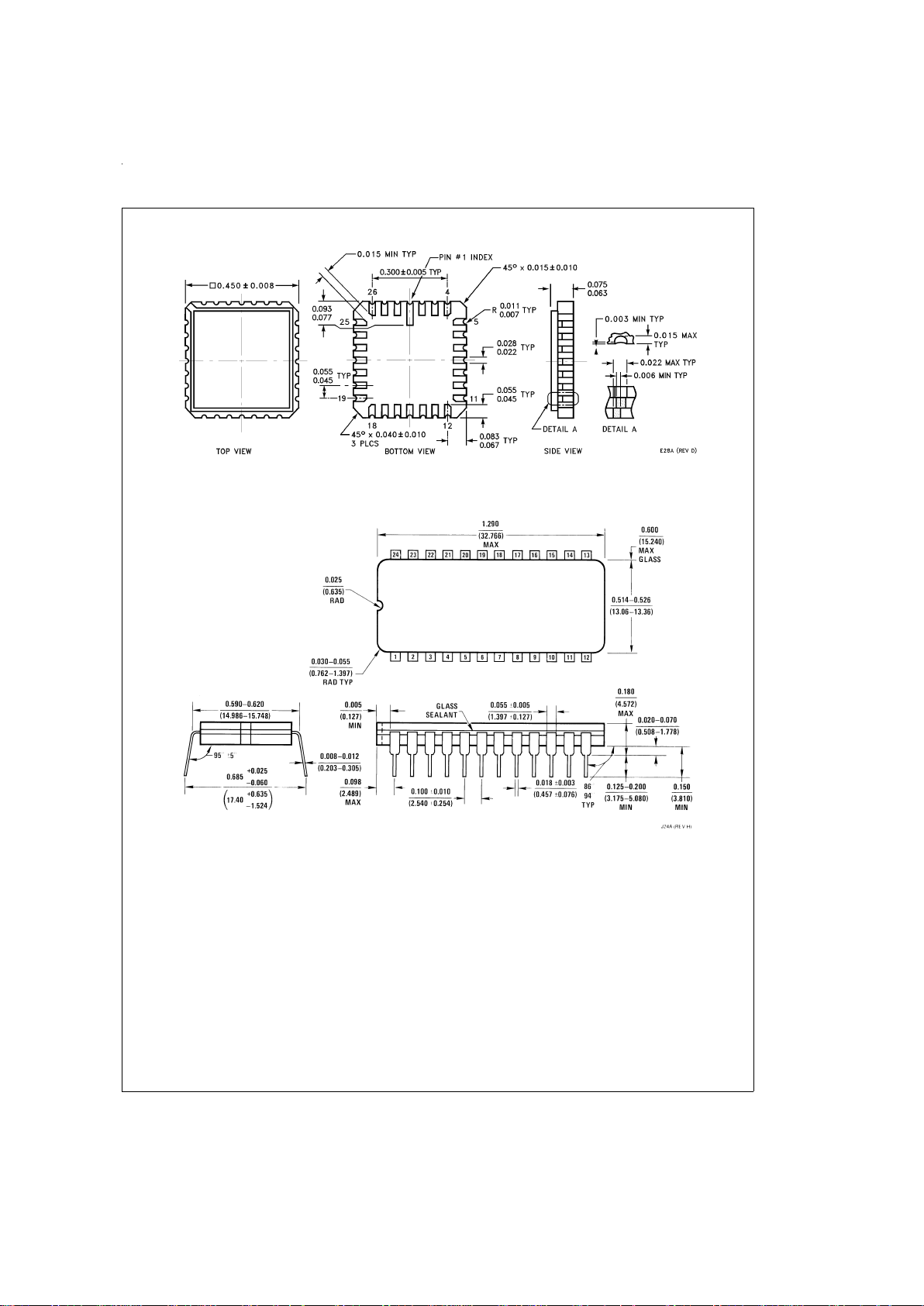
Physical Dimensions inches (millimeters) unless otherwise noted
28-Lead Ceramic Leadless Chip Carrier (L)
Order Number 54ABT543E-QML
NS Package Number E28A
24-Lead Ceramic Dual-In-Line Package
Order Number 54ABT543J-QML
NS Package Number J24A
7 www.national.com
Page 8
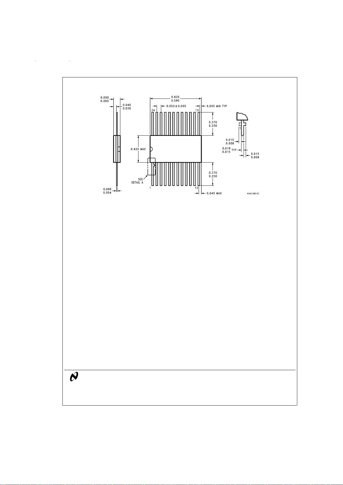
Physical Dimensions inches (millimeters) unless otherwise noted (Continued)
LIFE SUPPORT POLICY
NATIONAL’S PRODUCTS ARE NOT AUTHORIZED FOR USE AS CRITICAL COMPONENTS IN LIFE SUPPORT DEVICES OR SYSTEMS WITHOUT THE EXPRESS WRITTEN APPROVAL OF THE PRESIDENT OF NATIONAL SEMICONDUCTOR CORPORATION. As used herein:
1. Life support devices or systems are devices or systems which, (a) are intended for surgical implant into
the body, or (b)support orsustain life,and whosefailure to perform when properly used in accordance
with instructions for use provided in the labeling, can
be reasonably expected toresult ina significant injury
to the user.
2. A critical component in any component of a life support
device or system whose failure to perform can be reasonably expected tocause the failure of thelife support
device or system, orto affectits safety or effectiveness.
National Semiconductor
Corporation
Americas
Tel: 1-800-272-9959
Fax: 1-800-737-7018
Email: support@nsc.com
www.national.com
National Semiconductor
Europe
Fax: +49 (0) 1 80-530 85 86
Email: europe.support@nsc.com
Deutsch Tel: +49 (0) 1 80-530 85 85
English Tel: +49 (0) 1 80-532 78 32
Français Tel: +49 (0) 1 80-532 93 58
Italiano Tel: +49 (0) 1 80-534 16 80
National Semiconductor
Asia Pacific Customer
Response Group
Tel: 65-2544466
Fax: 65-2504466
Email: sea.support@nsc.com
National Semiconductor
Japan Ltd.
Tel: 81-3-5620-6175
Fax: 81-3-5620-6179
24-Lead Ceramic Flatpak Package (F)
Order Number 54ABT543W-QML
NS Package Number W24C
54ABT543 Octal Registered Transceiver with TRI-STATE Outputs
National does not assume any responsibility for use of any circuitry described, no circuit patent licenses are implied and National reserves the right at any time without notice to change said circuitry and specifications.
 Loading...