


Daewoo DLT-37C7, DLT-37C3, DLT-32C7, DLT-32C6, DLT-32C3 Service Manual
...S/M NO. : DSL500TEF0
Service Manual
LCD TV
CHASSIS : SL-500T
Model : DLT-26C2
DLT-26C3
DLT-32C1
DLT-32C2
DLT-32C3
DLT-32C6
DLT-32C7
DLT-37C3
DLT-37C7
Sep. 2007
Contents
1.Safety Precaution ………………………………………………………………………………… 3 2.Product Specification …………………………………………………………………………… 4 2-1.Product Specification………………………………………………………………………… 4 2-2.Available Input Signal ……………………………………………………………………… 5 3.Block Diagram …………………………………………………………………………………… 6 3-1.Block Diagram(Signal) ……………………………………………………………………… 6 3-2.Block Diagram(Power) ……………………………………………………………………… 7 4.Description of Each Block ……………………………………………………………………… 8 4-1.Block Diagram of Main IC and TP ………………………………………………………… 8
4-2.Overview ……………………………………………………………………………………… 9 4-2-1.Composite video, Y/C(S-Video) and SCART(CVBS, RGB) composite video … 9 4-2-2.DTV/DVD signal ……………………………………………………………………… 11 4-2-3.PC(Personal Computer)signal ……………………………………………………… 13 4-2-4.HDMI signal …………………………………………………………………………… 15 4-2-5.R/G/B Processing(SCART1, TELETEXT R/G/B) ………………………………… 15 4-2-6.Audio signal processing, KEY, and LED …………………………………………… 17
4-3.POWER PCB ………………………………………………………………………………… 21 5.SERVICE MODE ………………………………………………………………………………… 24 5-1.Entering SERVICE MODE ………………………………………………………………… 24 6.Main PCBs Trouble Diagnosis ………………………………………………………………… 26 6-1.Main PCBs Trouble Diagnosis ……………………………………………………………… 26 6-1-1.Common checking process when “No signal of Noraster” ……………………… 26 6-1-2.When No Sound ……………………………………………………………………… 33 6-1-3.When Control Key does not operate………………………………………………… 35 6-1-4.When Remote Controller does not operate ………………………………………… 36 6-2.POWER PCB ………………………………………………………………………………… 38 7.Trouble Diagnosis ………………………………………………………………………………… 39 7-1.Facts you must know when Diagnosis or Repairing……………………………………… 39 7-2.Typical Symptoms of PCB problem or bad connection ………………………………… 40 8.Structure of LCD Set …………………………………………………………………………… 41 9.Exploded View …………………………………………………………………………………… 43 10.Service Part List ………………………………………………………………………………… 52 11.Circuit Diagram ………………………………………………………………………………… 98
-2-

1.Safety Precautions
(1)When moving or laying down a LCD Set, please deal with care. Avoid any impact towards the LCD Set.
(2)Do not leave a broken LCD Set on for a long time. To prevent any further damages, after check the broken Set’s condition, make sure to turn the power (AC) off.
(3)When opening the BACK COVER, you must turn off power (AC) to prevent any electric shock.
(4)When loosening screws, check the connecting position and type of the screw.
Sort out the screws and store them separately
Because screws holding PCBs are working as electric circuit grounding, make sure to check if any screw is missing when assembling.
(5) A LCD Set contains different kinds of connector cables.
When connecting or disconnecting connector cables, check the direction and position of the cable beforehand.
(6)When disconnecting connectors unplug the connectors slowly with care.
(7)Connectors are designed so that if the number of pins or the direction does not match, connectors will not fit.
When having problem in plugging the connectors, make sure to check their kind, position, and direction.
-3-

2. Product Specification
2-1.PRODUCT SPECIFCATION
Features |
DLT-26C2SMDB |
DLT-32C6LMBD |
DLT-32C6SMBD |
DLT-37C3LMBD |
|
|
|
|
|
|
|
|
Screen Size |
26” |
32” |
32” |
37” |
|
|
|
|
|
|
|
Aspect Ratio |
16 : 9 |
16 : 9 |
16 : 9 |
16 : 9 |
LCD Panel |
|
|
|
|
|
Resolution |
1366x768(WXGA) |
1366x768(WXGA) |
1366x768(WXGA) |
1366x768(WXGA) |
|
|
|
||||
|
|
|
|
|
|
|
Pixel Pitch |
0.421(H) x |
170.25um x |
0.51075(H) x |
0.200mm x |
|
|
0.140(W)*3mm |
510.75um x RGB |
0.17025(W)*3 |
0.600mm x RGB |
|
Contrast |
1200 : 1 |
800 : 1 |
800 : 1 |
800 : 1 |
|
Ratio |
|
|
|
|
|
Receiving |
PAL, SECAM |
PAL, SECAM |
PAL, SECAM |
PAL, SECAM |
|
System |
||||
|
|
|
|
|
|
|
|
|
|
|
|
TV System |
Stereo |
FM MONO / |
FM MONO / |
FM MONO / |
FM MONO / |
System |
2-Carrier, NICAM |
2-Carrier, NICAM |
2-Carrier, NICAM |
2-Carrier, NICAM |
|
|
|
|
|
|
|
|
Channel |
ANALOG : 0~99CH |
ANALOG : 0~99CH |
ANALOG : 0~99CH |
ANALOG : 0~99CH |
|
Memory |
||||
|
|
|
|
|
|
|
RF |
75 Ohm Coaxial |
75 Ohm Coaxial |
75 Ohm Coaxial |
75 Ohm Coaxial |
|
|
|
|
|
|
|
S-Video |
1 |
1 |
1 |
1 |
|
|
|
|
|
|
Input |
SCART |
2 |
2 |
2 |
2 |
|
|
|
|
|
|
|
|
|
|
|
|
Connector |
Component |
RCA X 1 |
RCA X 1 |
RCA X 1 |
RCA X 1 |
|
|
|
|
|
|
|
PC RGB |
D-Sub X 1 |
D-Sub X 1 |
D-Sub X 1 |
D-Sub X 1 |
|
|
|
|
|
|
|
PC Audio |
3.5mm Mini-Jack |
3.5mm Mini-Jack |
3.5mm Mini-Jack |
3.5mm Mini-Jack |
|
|
|
|
|
|
|
HDMI |
1 |
1 |
1 |
1 |
|
|
|
|
|
|
Output |
Headphone |
3.5mm Mini-Jack |
3.5mm Mini-Jack |
3.5mm Mini-Jack |
3.5mm Mini-Jack |
Connector |
|||||
|
|
|
|
|
|
Sound |
|
10W |
10W |
10W |
10W |
Output |
|
||||
|
|
|
|
|
|
Power |
Max |
100W |
115W |
135W |
150W |
|
|
|
|
|
|
Consumption |
Power |
180VAC ~ 264VAC, |
180VAC ~ 264VAC, |
180VAC ~ 264VAC, |
180VAC ~ 264VAC, |
|
Source |
50~60Hz |
50~60Hz |
50~60Hz |
50~60Hz |
|
|
|
|
|
|
Dimension |
Set |
812 x 502.7 x 240 |
806 x 628.5 x 250 |
806 x 628.5 x 250 |
940 x 720 x 328.7 |
(W x H x D) |
Dimension |
||||
|
|
|
|
|
|
|
|
|
|
|
|
-4-

Product Specification
2-2.Available Input Signal
2-2-1.HDMI/PC/COMPONENT
Resolution |
V-freg |
HDMI |
PC(D-Sub) |
Component |
Standard |
|
|
|
|
|
|
|
60Hz |
O |
O |
X |
|
640 x 480 |
|
|
|
|
|
72Hz |
O |
O |
X |
|
|
|
|
|
|
|
|
|
75Hz |
O |
O |
X |
VESA Standard |
|
|
|
|
|
|
|
60Hz |
O |
O |
X |
VESA Standard |
800 x 600 |
|
|
|
|
|
72Hz |
O |
O |
X |
VESA Standard |
|
|
|
|
|
|
|
|
75Hz |
O |
O |
X |
|
|
|
|
|
|
|
|
60Hz |
O |
O |
X |
VESA Standard |
1024 x 768 |
|
|
|
|
|
70Hz |
O |
O |
X |
VESA Standard |
|
|
|
|
|
|
|
|
75Hz |
O |
O |
X |
VESA Standard |
|
|
|
|
|
|
1360 x 768 |
60Hz |
O |
O |
X |
|
|
|
|
|
|
|
75Hz |
O |
O |
X |
|
|
|
|
||||
|
|
|
|
|
|
720 x 480 |
60Hz |
O |
X |
O |
|
|
|
|
|
|
|
720 x 576 |
50Hz |
O |
X |
O |
|
|
|
|
|
|
|
1280 x 720 |
50Hz |
O |
O |
O |
|
|
|
|
|
|
|
60Hz |
O |
O |
O |
|
|
|
|
||||
|
|
|
|
|
|
1920 x 1080i |
50Hz |
O |
X |
O |
|
|
|
|
|
|
|
60Hz |
O |
X |
O |
|
|
|
|
||||
|
|
|
|
|
|
720 x 480i |
60Hz |
X |
X |
O |
|
|
|
|
|
|
|
720 x 576i |
50Hz |
X |
X |
O |
|
|
|
|
|
|
|
2-2-2.VIDEO
-PAL, PAL-M, PAL-N
-NTSC, NTSC4.43
-SECAM
-5-

3. Block Diagram
3-1.Block Diagram(Signal) |
-6- |
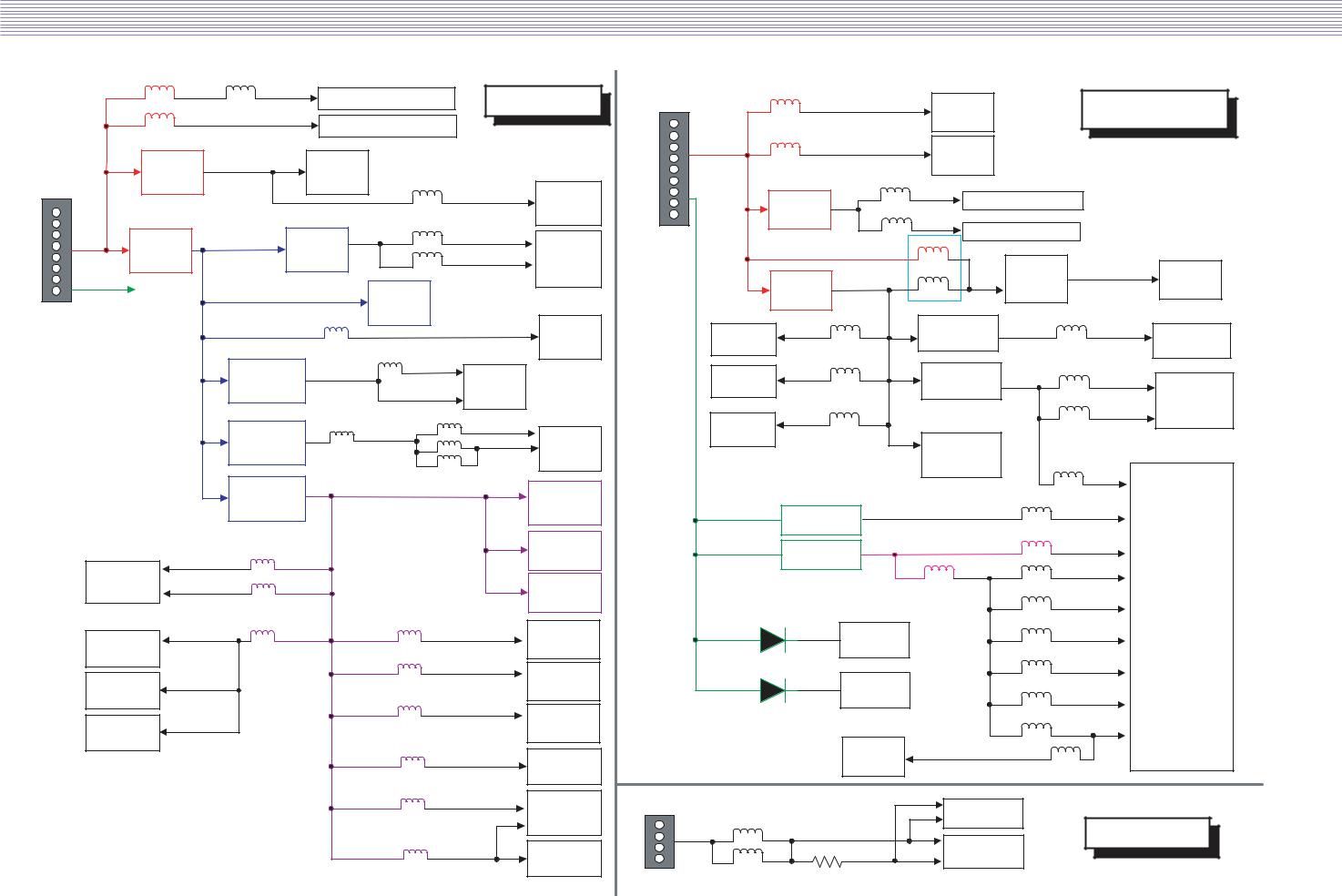
Block Diagram
3-2.Block Diagram(Power)
-7-
4. Description of Each Block
4-1.Block Diagram of Main IC and TP
-8- |
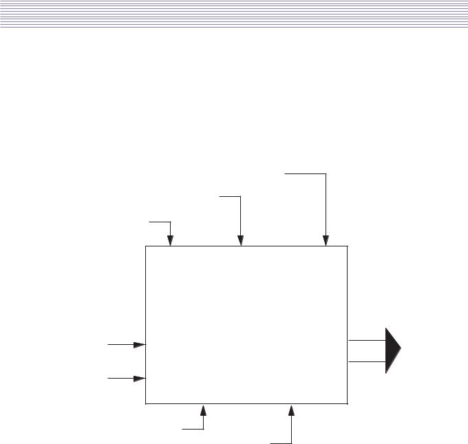
Description of Each Block
4-2.Overview
Digital PCB is Multi Media circuit board that can process carious input signals such as Video, component, PC, HDMI, and analog TV signal.
4-2-1.Composite video, Y/C(S-Video) and SCART(CVBS, RGB) composite video -Flow Chart of RF, Video, S-Video Signal
Y-pb-pr
AV3-Y/C
Scart1-rgb-fb
Tuner Cvbs 
Scart1-Cvbs  U8
U8
MST96889LD
Scart1-Cvbs |
|
AV3-Cvbs |
LVDS |
|
R-G-B
HY HDMI
TMDS-IN
-9-
Description of Each Block
Y signal(input to U8)
Location:R199
Color signal(input to U8)
Location:R173
-10-
Description of Each Block
CVBS signal(input to U8)
Location:R203
4-2-2.DTV/DVD signal
Y signal(input to U8)
Location:R171
-11-
Description of Each Block
PB signal(input to U8)
Location:R193
Pr signal(input to U8)
Location:R167
-12-
Description of Each Block
4-2-3.PC(Personal Conputer) signal
R signal(input to U8)
Location:R150
G signal(input to U8)
Location:R149
B signal(input to U8)
Location:R147
-13-
Description of Each Block
Horizontal sync(Output of U8) Location:R89
Vertical sync(Output of U13)
Location:R91
-14-
Description of Each Block
4-2-4.HDMI signal
Location:R62, R63, R64, R65, R66, R67, R68, R69
4-2-5.R/G/B PROCESSING(SCART 1, TELETEXT R/G/B)
R signal(input to U8)
Location:R159
-15-
Description of Each Block
G signal(input to U8)
Location:R156
B signal(input to U8)
Location:R184
-16-
Description of Each Block
4-2-6.Audio signal processing, KEY, and LED -Flow Chart of Audio Signal
RF(SIF) |
SC1 |
SC2 |
AV3 |
COMP |
PC |
|
12S |
U1 |
|
SC1-OUT |
|
|
|
||||
|
|
W M 8521 |
|
|
Speaker L & |
|
|
|
|
|
|
|
|
|
|
|
|
|
Sound L |
|
|
|
Headphone L |
U8 |
|
|
U12 |
||
|
|
|
|||
|
|
|
TDA8931T |
|
|
M ST96889LD |
|
U13 |
|
|
|
|
|
|
Speaker R& |
||
|
Sound R |
TDA1308 |
|
|
|
|
|
U14 |
Headphone R |
||
|
|
|
|
|
|
|
|
|
|
TDA8931T |
|
|
|
|
|
|
|
|
|
|
|
|
|
HDMI
Pre AMP input
Location:CE38, CE39
-17-
Description of Each Block
U12, U14 input
Location:CE33, CE43
U12, U14 output
Location:C199, C215
-18-
Description of Each Block
SIF input
Location:R124
I2S input
Location:R19(CLK)
-19-
Description of Each Block
Location:R20
Remote control signal
Location:L73
-20-
Description of Each Block
4-3.Power PCB
4-3-1.Power Spec -Rating:180V ~ 264V -Regulating Method:
-Input Frequency : 50/60Hz
-Inrush Current : Below 80A at AC 230V -Output Voltage and Current are shown below
26” & 32”
Board |
|
Output |
Minimum |
|
Maxmum |
|
|
Output Current |
Condition |
||||||
|
Output |
|
|
Output |
|
|
|
|
|
|
|||||
|
Voltage |
|
|
|
MIN |
|
NOR |
MAX |
|||||||
|
|
Voltage |
|
Voltage |
|
|
|
||||||||
|
|
|
|
|
|
|
|
|
|
|
|
||||
|
|
|
|
|
|
|
|
|
|
|
|
|
|
|
|
|
|
+29Vdc |
+27.0Vdc |
|
+32.0Vdc |
|
0.1A |
|
0.5A |
0.7A |
|
||||
|
|
|
|
|
|
|
|
|
|
|
|
|
|
|
|
|
|
+24Vdc |
+22.3Vdc |
|
+25.4Vdc |
|
0.3A |
|
5.2A |
6.0A |
PWR-CTL |
||||
|
|
|
|
|
|
|
|
|
|
|
|
|
|
|
|
DEP |
|
+12Vdc |
+11.0Vdc |
|
+12.0Vdc |
|
0.3A |
|
1.2A |
2.0A |
ON |
||||
|
|
|
|
|
|
|
|
|
|
|
|
|
|
|
|
|
|
+ 5Vdc |
+4.75Vdc |
|
+5.25Vdc |
0.1A |
|
1.5A |
2.0A |
|
|||||
|
|
|
|
|
|
|
|
|
|
|
|
|
|
|
|
|
|
ST+5Vdc |
+4.75Vdc |
|
+5.25Vdc |
0.1A |
|
0.2A |
0.3A |
PWR-CTL |
|||||
|
|
|
|
OFF |
|||||||||||
|
|
|
|
|
|
|
|
|
|
|
|
|
|
|
|
|
|
|
|
|
|
|
|
|
|
|
|
|
|
|
|
37” |
|
|
|
|
|
|
|
|
|
|
|
|
|
|
|
|
|
|
|
|
|
|
|
|
|
|
|||||
Board |
|
Output |
Minimum |
|
Maxmum |
|
|
Output Current |
Condition |
||||||
|
Output |
|
|
Output |
|
|
|
|
|
|
|||||
|
Voltage |
|
|
|
MIN |
|
NOR |
MAX |
|||||||
|
|
Voltage |
|
Voltage |
|
|
|
||||||||
|
|
|
|
|
|
|
|
|
|
|
|
||||
|
|
|
|
|
|
|
|
|
|
|
|
|
|
||
|
|
+29Vdc |
+27.0Vdc |
|
+32.0Vdc |
|
0.1A |
|
0.5A |
0.7A |
|
||||
|
|
|
|
|
|
|
|
|
|
|
|
|
|
||
|
|
+24Vdc |
+22.3Vdc |
|
+25.4Vdc |
|
0.3A |
|
5.6A |
6.5A |
PWR-CTL |
||||
|
|
|
|
|
|
|
|
|
|
|
|
|
|
|
|
DEP |
|
+12Vdc |
+11.0Vdc |
|
+12.0Vdc |
|
0.3A |
|
1.2A |
2.0A |
ON |
||||
|
|
|
|
|
|
|
|
|
|
|
|
|
|
|
|
|
|
+ 5Vdc |
+4.75Vdc |
|
+5.25Vdc |
0.1A |
|
1.5A |
2.0A |
|
|||||
|
|
|
|
|
|
|
|
|
|
|
|
|
|
|
|
|
|
ST+5Vdc |
+4.75Vdc |
|
+5.25Vdc |
0.1A |
|
0.2A |
0.3A |
PWR-CTL |
|||||
|
|
|
|
OFF |
|||||||||||
|
|
|
|
|
|
|
|
|
|
|
|
|
|
|
|
|
|
|
|
|
|
|
|
|
|
|
|
|
|
|
|
-Ripple and Noise |
|
|
|
|
|
|
|
|
|
|
|
|
|||
|
|
|
|
|
|
|
|
|
|
|
|||||
|
|
|
|
Output Valtage |
AC ripple, switching ripple |
|
|||||||||
Output |
|
|
and noise |
|
|
Condition |
|||||||||
|
|
|
|
|
|
|
|
|
|||||||
|
|
|
|
|
|
|
|
|
|
|
|
|
|||
|
Minimum |
|
Maxmum |
|
|
|
|
|
|
||||||
Name |
|
|
|
Continuous |
|
|
|
||||||||
|
|
|
Output Voltage |
|
Output Voltage |
|
|
|
|
|
|
|
|||
+29V |
|
+27.0Vdc |
|
+32.0Vdc |
|
|
|
|
|
|
|
||||
|
|
|
|
|
|
|
|
|
|
|
|
||||
+24V |
|
+22.3Vdc |
|
+25.4Vdc |
|
|
500mVp-p |
|
|
PWR-CTR |
|||||
|
|
|
|
|
|
|
|
|
|
|
|
|
|||
+12V |
|
+11.0Vdc |
|
+12.0Vdc |
|
|
|
|
ON |
||||||
|
|
|
|
|
|
|
|
||||||||
|
|
|
|
|
|
|
|
|
|
|
|
||||
+ 5V |
|
+4.75Vdc |
|
+5.25Vdc |
|
|
|
|
|
|
MAX LOAD |
||||
|
|
|
|
|
|
|
|
|
|
|
|||||
ST+5V |
|
+4.75Vdc |
|
+5.25Vdc |
|
|
500mVp-p |
|
|
PWR-CTL |
|||||
|
|
|
|
Other Lines |
|
|
|
Don’t Care |
|
|
OFF |
||||
|
|
|
|
|
|
|
|
|
|
||||||
|
|
|
|
|
|
|
|
|
|
|
|
|
|
|
|
-21-

Description of Each Block
4-3-2.Connectors
A. CN7, CN8 pin Spec(YEON-HO 20010WS-14 14P) |
|
||||||||||||
|
|
CN7(AUO PANNEL) |
CN8(SAMSUNG PANNEL) |
||||||||||
|
|
|
|
|
|
|
|
|
|
|
|
|
|
|
|
|
|
PIN No. |
Output |
|
|
|
PIN No. |
Output |
|||
|
|
|
|
|
|
|
|
|
|
|
|
|
|
|
|
|
|
|
|
|
|
|
|
|
|
1 |
+24V |
|
|
|
1 |
|
+24V |
|
|
||||||
|
|
|
|
|
|
|
|
|
|
|
|
|
|
|
|
|
|
|
|
|
|
|
|
|
|
2 |
+24V |
|
|
|
2 |
|
+24V |
|
|
||||||
|
|
|
|
|
|
|
|
|
|
|
|
|
|
|
|
|
|
|
|
|
|
|
|
|
|
3 |
+24V |
|
|
|
3 |
|
+24V |
|
|
||||||
|
|
|
|
|
|
|
|
|
|
|
|
|
|
|
|
|
|
|
|
|
|
|
|
|
|
4 |
+24V |
|
|
|
4 |
|
+24V |
|
|
||||||
|
|
|
|
|
|
|
|
|
|
|
|
|
|
|
|
|
|
|
|
|
|
|
|
|
|
5 |
+24V |
|
|
|
5 |
|
+24V |
|
|
||||||
|
|
|
|
|
|
|
|
|
|
|
|
|
|
|
|
|
|
|
|
|
|
|
|
|
|
6 |
GND |
|
|
|
6 |
|
GND |
|
|
||||||
|
|
|
|
|
|
|
|
|
|
|
|
|
|
|
|
|
|
|
|
|
|
|
|
|
|
7 |
GND |
|
|
|
7 |
|
GND |
|
|
||||||
|
|
|
|
|
|
|
|
|
|
|
|
|
|
|
|
|
|
|
|
|
|
|
|
|
|
8 |
GND |
|
|
|
8 |
|
GND |
|
|
||||||
|
|
|
|
|
|
|
|
|
|
|
|
|
|
|
|
|
|
|
|
|
|
|
|
|
|
9 |
GND |
|
|
|
9 |
|
GND |
|
|
||||||
|
|
|
|
|
|
|
|
|
|
|
|
|
|
|
|
|
|
|
|
|
|
|
|
|
|
|
GND |
|
|
|
10 |
|
GND |
|
|
10 |
|||||
|
|
|
|
|
|
|
|
|
|
|
|
|
|
|
|
|
|
|
|
|
|
|
|
|
|
11 |
N/C |
|
|
|
11 |
|
DIMIMING |
|
|
||||||
|
|
|
|
|
|
|
|
|
|
|
|
|
|
|
|
|
|
|
|
|
|
|
|
|
|
12 |
INV ON/OFF |
|
|
|
12 |
|
INV ON/OFF |
|
|
||||||
|
|
|
|
|
|
|
|
|
|
|
|
|
|
|
|
|
|
|
|
|
|
|
|
|
|
13 |
DIMIMING |
|
|
|
13 |
|
N/C |
|
|
||||||
|
|
|
|
|
|
|
|
|
|
|
|
|
|
|
|
|
|
|
|
|
|
|
|
|
|
14 |
N/C |
|
|
|
14 |
|
GND |
|
|
||||||
|
|
|
|
|
|
|
|
|
|
|
|
||
|
|
|
|
|
|
|
|
|
|
|
|
|
|
B. CN5, CN6 pin Spec(YEON-HO 20010WS-12 12P) |
|
||||||||||||
CN5,CN6(LG PANNEL) |
|
|
|
|
|||||||||
|
|
|
|
|
|
|
|
|
|
|
|
|
|
|
|
|
|
PIN No. |
|
Output |
|
|
|
|
|
||
|
|
|
|
|
|
|
|
|
|
|
|||
|
1 |
|
+24V |
|
|
|
|
|
|||||
|
|
|
|
|
|
|
|
|
|
|
|||
|
2 |
|
+24V |
|
|
|
|
|
|||||
|
|
|
|
|
|
|
|
|
|
|
|||
|
3 |
|
+24V |
|
|
|
|
|
|||||
|
|
|
|
|
|
|
|
|
|
|
|||
|
4 |
|
+24V |
|
|
|
|
|
|||||
|
|
|
|
|
|
|
|
|
|
|
|||
|
5 |
|
+24V |
|
|
|
|
|
|||||
|
|
|
|
|
|
|
|
|
|
|
|||
|
6 |
|
GND |
|
|
|
|
|
|||||
|
|
|
|
|
|
|
|
|
|
|
|||
|
7 |
|
GND |
|
|
|
|
|
|||||
|
|
|
|
|
|
|
|
|
|
|
|||
|
8 |
|
GND |
|
|
|
|
|
|||||
|
|
|
|
|
|
|
|
|
|
|
|||
|
9 |
|
GND |
|
|
|
|
|
|||||
|
|
|
|
|
|
|
|
|
|
|
|||
|
10 |
|
GND |
|
|
|
|
|
|||||
|
|
|
|
|
|
|
|
|
|
|
|||
|
11 |
|
DIMIMING |
|
|
|
|
|
|||||
|
|
|
|
|
|
|
|
|
|
|
|||
|
12 |
|
INV ON/OFF |
|
|
|
|
|
|||||
|
|
|
|
|
|
|
|
|
|
|
|
|
|
-22-

Description of Each Block
C.CN2 Pin Spec(YEON-HO YW025-04 4P)
PIN No. |
Output |
|
|
1 |
+29V |
|
|
2 |
+29V |
|
|
3 |
GND |
|
|
4 |
GND |
|
|
D.CN4 Pin Spec(YEON-HO SMW025-09 9P)
PIN No. |
Output |
|
|
1 |
+12V |
|
|
2 |
+12V |
|
|
3 |
GND |
|
|
4 |
GND |
|
|
5 |
+5VS |
|
|
6 |
PWR ON/OFF |
|
|
7 |
GND |
|
|
8 |
GND |
|
|
9 |
+5VS |
|
|
E.CN3 Pin Spec(CA3237W-300-08P)
PIN No. |
Output |
|
|
1 |
DIMIMING |
|
|
2 |
INV ON/OFF |
|
|
3 |
N/C |
|
|
4 |
GND |
|
|
5 |
GND |
|
|
6 |
+5VS |
|
|
7 |
+5VS |
|
|
8 |
+12V |
|
|
-23-

5. SERVICE MODE
5-1.Entering SERVICE MODE
Using the Service Remote controller, you can enter service mode directly.
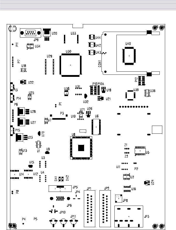
|
5-1-1.Adjustment REMOCON and EEPROM Initial DATA |
||||||
|
A.The adjustment Specification use the SERVICE REMOCON R-34SVC |
||||||
|
(S/N:48B3034SVC) |
|
|
|
|||
|
B.Adjustment DATA |
|
2007. 05. 11 |
||||
|
|
|
|
|
|
|
|
Key |
Menu |
Sub Menu |
Default Value |
Description |
|||
S1 |
Heat Run Mode |
|
Full White |
to enter into Heat Run Mode |
|||
|
|
|
|
|
|
|
|
S2 |
Gumi Ch Map Write |
|
|
to set Gumi factory channels directly |
|||
|
|
|
|
|
|
|
|
S3 |
Volume Test |
|
0-50-100-L-R |
to set sound(display in sequence) |
|||
|
|
|
|
|
|
|
|
S4 |
HDMI EDID WRITE |
|
|
to write HDMI EDID data directly from main chip |
|||
|
|
|
|
|
|
|
|
S5 |
Test Pattem |
|
Black-W-R-G-B |
to display Test Pattem in sequence |
|||
|
|
|
|
|
|
|
|
|
|
|
|
|
Bri_Min-Cen-Max |
to test picture(displays in sequence) |
|
S6 |
|
|
|
|
|
|
|
Picture Test |
|
Con_Min-Cen-Max |
to test picture(displays in sequence) |
||||
|
|
|
|
|
|
|
|
|
|
|
|
|
Col_Min-Cen-Max |
to test picture(displays in sequence) |
|
|
|
|
|
|
|
|
|
S7 |
DEMPOL CH Map Write |
|
|
to test picture(displays in sequence) |
|||
|
|
|
|
|
|
|
|
|
|
|
|
input Source Display |
|
to display present input source mode |
|
|
|
|
|
|
|
|
|
|
|
|
|
Offset R |
32 |
|
|
|
|
|
|
|
|
|
|
|
|
|
|
Offset G |
32 |
|
|
|
|
|
|
|
|
|
|
|
|
|
|
Offset B |
32 |
|
|
S8 |
Write Balance |
|
|
|
|
to display offset and gain value at mode above |
|
|
|
Gain R |
32 |
||||
|
|
|
|
|
|
|
|
|
|
|
|
Gain G |
32 |
|
|
|
|
|
|
|
|
|
|
|
|
|
|
Gain B |
32 |
|
|
|
|
|
|
|
|
|
|
|
|
|
|
Read Value |
32 |
to display the matched real value of the offset |
|
|
|
|
|
and gain |
|||
|
|
|
|
|
|
||
|
|
|
|
|
|
|
|
|
|
|
|
Speaker_SIF |
32 |
|
|
|
|
|
|
|
|
|
|
|
|
|
|
Speaker_AV3 DVB |
37 |
|
|
|
|
|
|
|
|
|
|
|
|
|
|
Speaker_AV2 |
43 |
|
|
|
|
|
|
|
|
||
|
Sound Prescale |
Speaker_HDMI |
47 |
to display sound prescale value at each mode |
|||
|
|
|
|
|
|
|
|
|
|
|
|
Speaker_AV1 PC COM |
55 |
|
|
|
|
|
|
|
|
|
|
S9 |
|
|
|
Scartout_SIF |
88 |
|
|
|
|
|
|
|
|
|
|
|
|
|
Scartout_EXCEPTSIF |
88 |
|
|
|
|
|
|
|
|
|
||
|
|
|
|
|
|
|
|
|
|
|
|
Delay Enable |
OFF |
to active or inactive sound delay mode |
|
|
Sound Delay |
|
|
|
|||
|
Delay value |
0 |
to assign delay value |
||||
|
|
|
|
|
|
|
|
|
|
|
|
Apply |
|
to apply the changed value about sound delay |
|
|
Dimming Control |
|
254 |
to control the dimming value of the panel |
|||
|
|
|
|
IFAGC NORMAL |
18 |
to adjust IF AGC value about signal except |
|
|
IFAGC Contronl |
SECAM L/L’ |
|||||
|
|
|
|||||
|
|
|
|
IFAGC L or L’ |
16 |
to adjust IF AGC value about SECAM L/L’ |
|
|
Frequency |
|
000 MHz |
to display the frequency of the present signal |
|||
|
Gamma |
|
OFF |
to active or inactive gamma function |
|||
|
DLC |
|
OFF |
to active or inactive DLC function |
|||
|
Memory Recall |
|
|
to reset EEPROM |
|||
|
Oper Mode |
|
NOR-DEB-DW |
Normal Mode-Debug Mode-Data Writing Mode |
|||
S10 |
Don’t use |
|
|
|
|
||
S11 |
Version information |
|
|
to display the date of the firm ware |
|||
S12 |
Factory Mode |
|
|
to initialize TV and make TV standby mode |
|||
|
|
¡White Balance items(S8) are not initialized |
|||||
|
|
|
|
|
|
||
|
|
|
|
|
|
|
|
-24-

SERVICE MODE
5-1-2.Description of SERVICE MODE ITEM A.S1(1) : Heat-Run Key
B.S2(2) : Gumi Channel Map Write C.S3(3) : Volume Test
=> This key can check sound D.S4(4) : EDIT WRITE
=> Using this key, you can up data EDID data. (but the “shunt”must be connected, and only executed in the Factory.)
E.S5(5) : PANEL TEST
=> Using this key, you can test problem of PANEL, as confirm white pattern red pattern, blue pattern, green pattern.
F.S6(6) : PICTURE TEST
=> Using this key, you can test brightness, contrast and color. G.S7(7): DEMPOL CHANNEL MAP WRITE
H.S8(8) : White Balance adjustment
=> Using this key, you can adjust White balance. I.S9(9) : Device control
=> This key only use for R&D. J.S10(10) : Opion key
=> Using this key, you can adjust SSC, Dimming, panel Type and etc. K.S11(11) : Version key
=>Using this key, you can identify the information of the S/W of the set. L.S12(SLEEP ) : Shipping key
=> Using this key, you can up at shipping mode.
-25-
6. Main PCBs Trouble Diagnosis
6-1.Main PCB Trouble Diagnosis
6-1-1.Common checking process when “No signal of Noraster” No signal : OSD is work but no images are displying
No raster : OSD as well as images in not working
Check start
Does No signal |
N |
|
|
screen appear? |
|
Y
Is the signal |
N |
|
Check the connection |
|
|
of Jack |
|
input Jack properly? |
|
|
|
|
|||
|
|
(LCD and AV device) |
|
|
|
|
|
|
|
|
|
Y
Does input source |
N |
|
||
Check AV device |
||||
|
|
|||
(AV device) work? |
|
|
||
|
||||
|
|
|
||
|
|
|
|
|
Y
N
Is input selection
Check input mode
in the Correct mode?
Y
Replace Main PCB and/or Sub PCB
Is a weak |
N |
Discharge detected |
|
|
|
in the screen? |
|
Y
N
Is LVDS connection Correctly connected?
Y
N
Is waveform of CLK in the Main PCB
Normal?
Y
Check other PCBs and connectors
1.Check AC connection 2.Check Power S/W ON 3.Check other PCBs
Check LVD connection Panel & P3 of Main PCB
Replace Main PCB and/or Sub PCB
-26-
Main PCBs Trouble Diagnosis
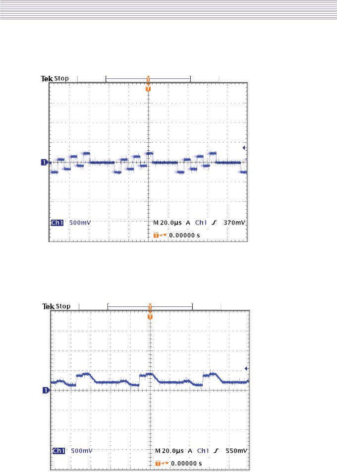
A.When “No signal”in CVBS(RF, AV) 1)First check if other inputs are working
=>if other inputs are not working, replace MAIN PCB
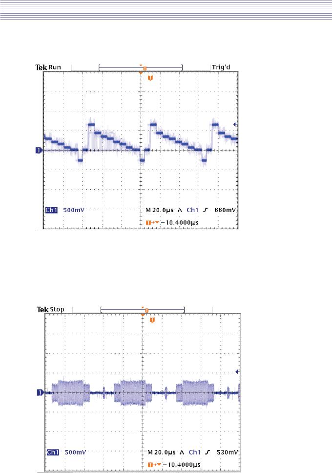
2)Checking waveforms with Color Bar Pattern(Using the oscilloscope) - Main TP(RF) : R203
- Main TP(RF) : R177
-27-

Main PCBs Trouble Diagnosis
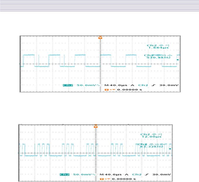
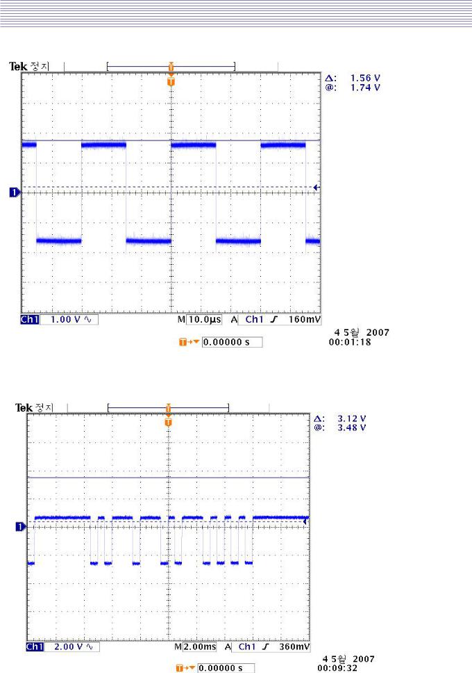
B.When “No signal”in Y/C signal(S-Video) 1)First check if other inputs are working
=>if other inputs are not working, replace MAIN PCB
2)Checking waveforms with Color Bar Pattern(Using the oscilloscope) - Main TP(Y signal) : R199
- Main TP(C signal) : R173
-28-
Main PCBs Trouble Diagnosis
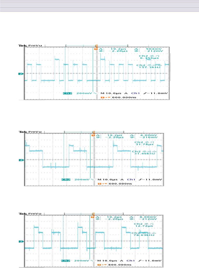
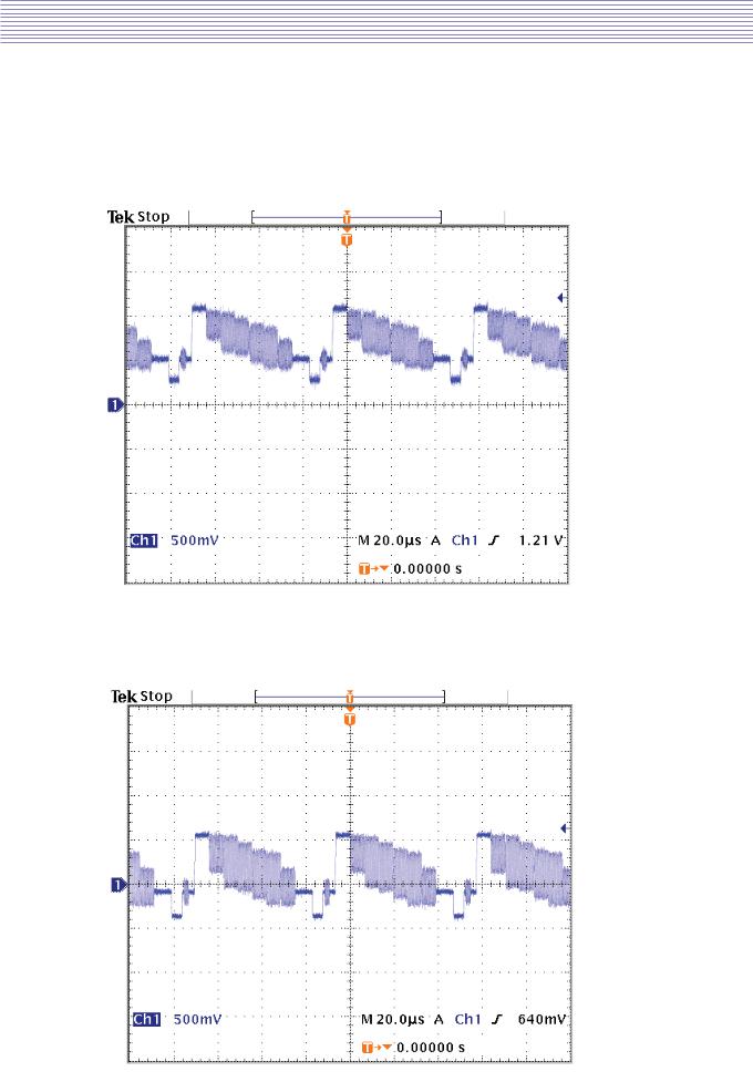
C.When “No signal”in Y/Pb/Pr signal(Component) 1)First check if other inputs are working
=>if other inputs are not working, replace MAIN PCB
2)Checking waveforms with Color Bar Pattern(Using the oscilloscope) - Main TP(COMP1- Y) : R171
- Main TP(COMP1-Pb) : R193
-29-
Main PCBs Trouble Diagnosis
- Main TP(COMP1-Pr) : R167
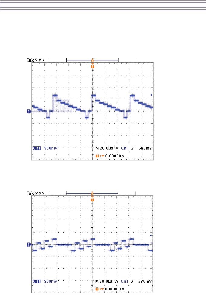
D.When “No signal”in PC
1)First check if other inputs are working
=>if other inputs are not working, replace MAIN PCB
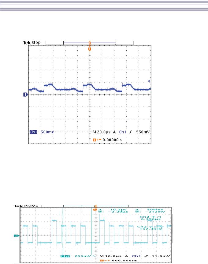
2)Checking waveforms with Color Bar Pattern(Using the oscilloscope) - Main TP(R signal) : R150
-30-
 Loading...