

SERVICE MANUAL
ABUSH 2114 2020 2321
COLOUR TELEVISION 11AK01 chassis
h911917

HINARI

SPECIFICATIONS
| TV BROADCAST STANDARD | PAL 1 CCIR | |
|---|---|---|
| RECEIVING CHANNELS |
UHF (BAND | & III)
UHF (BAND U) |
2114
2114 |
| UHF (BAND U) | 2020/2321 | |
| NUMBER OF PRESET CHANNELS | 39 | |
| CHANNEL INDICATOR | LED DISPLAY | |
| RF AERIAL INPUT | 75 OHM (UNBALANCED | )) |
| PICTURE TUBES |
14" PIL 90°
20" PIL 90° 21" FST PIL 90° |
2114
2020 2321 |
| SPEAKER | 8 OHM | |
| AUDIO OUTPUT POWERS | 1.5W (MAX) | |
| OPERATING VOLTAGES | 180-270V AC 50 HZ | |
| POWER CONSUMPTIONS |
65W
85W 85W |
2114
2020 2321 |
| DIMENSIONS (MM) |
460X315X350
610X420X455 577X422X465 |
2114
2020 2321 |
| NET WEIGHTS (KG) |
12.5
22.5 22.5 |
2114
2020 2321 |
و
SAFETY INSTRUCTIONS
WARNING:
BEFORE SERVICING THIS CHASSIS, PLEASE READ THE "X-RAY RADIATION PRECAUTION", "SAFETY PRECAUTION" AND "PRODUCT SAFETY NOTICE" DESCRIBED BELOW.
X-RAY RADIATION PRECAUTION
- 1. Excessive high voltages can produce potentially hazardous X-RAY RADIATION. To avoid such hazards, the high voltage must not be above the specified limit. The nominal value of the high voltage of this receiver is 22.5KV at zero beam current (minimum brightness) under specified power source. The high voltage must not under any circumstances exceed 25.3V.
- 2. The only source of X-RAY RADIATION in this TV receiver is the picture tube. For continued X-RAY RADIATION protection, the replacement tube must be of the same type tube as that specified in the parts list.
SAFETY PRECAUTION
- 1. Potentials as high as 24,000 volts are present when this receiver is operating. Operation of the receiver outside the cabinet or with the back cover removed presents a shock hazard from the receiver.
- (a) Servicing should not be attempted by anyone who is not thoroughly familiar with the precuations necessary when working on high-voltage equipment.
- (b) Always discharge the picture tube anode to the CHASSIS GROUND to remove shock hazard before disconnecting the anode cap.
- (c) Completely discharge the high potential of the picture tube before handling. The picture tube is highly evacuated and if broken glass fragments will be violently expelled.
- 2. In the event of fuse replacement, it should be replaced with the fuse type specified in the chassis parts list.
- 3. When replacing parts or circuit boards, wind the lead wires around terminals before soldering
- 4. When replacing a high wattage resistor (oxide metal film resistor) in the circuit board the resistor should be mounted 10mm away from circuit board.
PRODUCT SAFETY NOTICE
Many electrical and mechanical parts in this chassis have special safety-related characteristics. These characteristics are often passed unnoticed by visual inspection and the X-RAY RADIATION protection afforded by them cannot necessarily be obtained by using replacement components rated for higher voltage, wattage, etc. Replacement parts which have these special safety charactersitics are identified by in this manual and its supplements.
Before replacing any of these components, read the parts list in this manual carefully. The use of substitute replacement parts which do not have the same safety characteristics as specified in the parts list may create X-RAY RADIATION.
3
SERVICING PRECAUTIONS
WARNING:
BEFORE SERVICING PRODUCTS COVERED BY THIS SERVICE MANUAL AND ITS SUPPLEMENTS AND ADDENDUMS READ AND FOLLOW THE SAFETY PRECAUTIONS ON PAGE 2 OF THIS PUBLICATION. NOTE: IF UNFORESEEN CIRCUMSTANCES CREATE CONFLICT BETWEEN THE FOLLOWING SERVICING PRECAUTIONS AND ANY OF THE SAFETY PRECAUTIONS ON PAGE 2 OF THIS PUBLICATION, ALWAYS FOLLOW THE SAFETY PRECAUTIONS. REMEMBER: SAFETY FIRST.
GENERAL SERVICING PRECAUTIONS
- 1. Always remove the product AC power cord from the AC power supply before:
- (a) Removing or installing any component, circuit board, module, or any other instrument assembly.
- (b) Disconnecting or reconnecting any instrument electrical plug or other electrical connection.
- (c) Connecting a test substitute component in parallel with an electrolytic capacitor in the instrument.
Caution: A wrong part substitution or incorrect plarity installation of electrolytic capacitors may result in an explosion hazard.
- (d) Discharging the picture tube anode
- 2. Test high voltage only by measuring it with an appropriate high voltage meter or other voltage measuring device (DVM, FETVOM, etc.) equipped with a suitable high voltage probe. Do not test high voltage by "drawing an arc".
- 3. Discharging the picture tube anode only by (a) first connecting one end of an insulated clip lead to the degaussing or CRT aquadag grounding system shield at the point where the picture tube socket ground lead is connected and then touching the other end of the insulated clip lead to the picture tube anode connection using an insulating handle to avoid personal contact with high voltage.
- 4. Do not spray any chemicals on or near this instrument or any of its assemblies.
3
- Unless specified otherwise in this service manual, clean electrical contacts with a pipe cleaner, cotton-lipped stick or comparable nonabrasive applicator: 10% (by volume) Acetone and 90% (by volume) isoproply alcohol (90%-99% strength). Unless specified otherwise in this service manual, lubrication of contacts is not required.
- 6. Do not apply AC power to this produce and/or any of its electrical assemblies unless all solidstate device heat sinks are correctly installed.
ELECTROSTATICALLY SENSITIVE (ES) DEVICES
Some semiconductor (solid state) devices can be easily damaged by static electricity. Such components are commonly called Electrostatically Sensitive (ES) Devices. Examples of typical ES devices are integrated circuits and some field-effect transistors and semiconductor "chip" components. The following techniques should be used to help reduce the incidence of component damage caused by static electricity.
- 1. Immediately before handling any semiconductor component or semiconductor-equipped assembly, discharge any electrostatic charge on your body by touching a known earth ground. Alternatively, obtain and wear a commercially available discharging wrist strap device, which should be removed for potential shock reasons prior to applying power to the unit under test.
- 2. After removing an electrical assembly equipped with ES devices, place the assembly on a conductive surface such as aluminium foil to prevent electrostatic charge buildup or exposure of the assembly
- 3. Only use a grounded-tip soldering iron to solder or unsolder ES devices
- 4. Only use an anti-static type solder removal device some solder removal devices not classified as "anti-static" can generate electrical charges sufficient to damage ES devices
- 5. Do not remove a replacement ES device from its protective package until immediately before you are ready to install it. (Most replacement ES devices are packaged with leads electrically shorted together by conductive foam, aluminium foil or comparable conductive material).
- 6. Do not use freon-propelled chemicals. These can generate electrical charges sufficient to damage ES devices
- 7. Immediately before removing the protective material from the leads of a replacment ES device, touch the protective material to the chassis or circuit assembly into which the device will be installed.
CAUTION: Be sure no power is applied to the chassis or circuit, and observe all other safety precautions.
8. Minimize bodily movement when handling unpackaged replacement ES devices. (Otherwise harmless movement such as the brushing together of your clothes fabric or the lifting of your foot from a carpeted floor can generate static electricity sufficient to damage an ES device).
GENERAL SOLDERING GUIDELINES
- 1. Use a grounded-tip, low-wattage soldering iron and appropriate tip size and shape that will maintain tip temperature within the range 500°F to 600°F.
- 2. Use an appropriate gauge of RMA resin-core solder composed of 60 parts tin/40 parts lead.
- 3. Ensure the soldering iron tip is clean and well tinned.
- 4. Thoroughly clean the surfaces to be soldered. Use a small wire-bristle (0.5", or 1.25 cm) brush with a metal handle. Do not use freenpropelled spray-on cleaners.
- 5. Use the following unsoldering techniques:
- a) Allow the soldering iron tip to reach normal temperature (500°F to 600°F).
- b) Heat the component lead until the solder melts.
- c) Remove the melted solder with an anti-static, suction-type solder removal device or with solder braid.
CAUTION: Work guickly to avoid overheating the circuit board printed foil.
- 6. Use the following soldering techniques:
- a) Allow the soldering iron tip to reach normal temperature (500°F to 600°F).
- b) First, hold the soldering iron tip and solder strand against the component lead until the solder melts.
- c) Quickly move the soldering iron tip to the junction of the component lead and the printed circuit foil, and hold it there only until the solder flows onto and around both the component lead and the foil.
CAUTION: Work quickly to avoid overheating the circuit board printed foil.
d) Closely inspect the solder area and remove any excess or splashed solder with a small wirebristle brush.
IC REMOVAL/REPLACEMENT
Some chassis circuit boards have slotted holes (oblong) through which the IC leads are inserted and then bent flat against the circuit foil. When holes are of the slotted type, the following technique should be used to remove and replace the IC. When working with boards using the familiar round hole, use the standard technique as outlined in paragraphs 5 and 6 above.
REMOVAL
- 1. Desolder and straighten each IC lead in one operation by gently prying up on the lead with the soldering iron tip as the solder melts.
- 2. Remove the melted solder with an anti-static suction-type solder removal device (or with solder braid) before removing the IC.
REPLACEMENT
- 1. Carefully insert the replacement IC in the circuit board.
- 2. Carefully bend each IC lead against the circuit foil pad and solder it.
,
3. Clean the soldered areas with a small wire-bristle brush, (it is not necessary to reapply coating to the areas).
POWER OUTPUT TRANSISTOR DEVICES REMOVAL / REPLACEMENT
- 1. Heat and remove all solder from around the transistor leads.
- 2. Remove the heatsink mounting screw where fitted.
- 3. Carefully remove the transistor and heat sink from the circuit board.
- 4. Insert new transistor in circuit board.
- 5. Solder each transistor lead, and clip off excees lead.
WARNING:
DUE TO HIGH VACUUM AND LARGE SURFACE AREA OF PICTURE TUBE. GREAT CARE MUST BE EXERCISED WHEN HANDLING THE PICTURE TUBE. ALWAYS LIFT THE PICTURE TUBE BY GRASPING IT FIRMLY AROUND FACEPLATE. NEVER LIFT THE TUBE BY ITS NECK. THE PICTURE TUBE MUST NOT BE SCRATCHED OR SUBJECTED TO EXCESSIVE PRESSURE AS A FRACTURE OF THE GLASS MAY RESULT IN AN IMPLOSION OF CONSIDERABLE VOILENCE WHICH CAN CAUSE PERSONAL INUJURY OR PROPERTY DAMAGE.
,
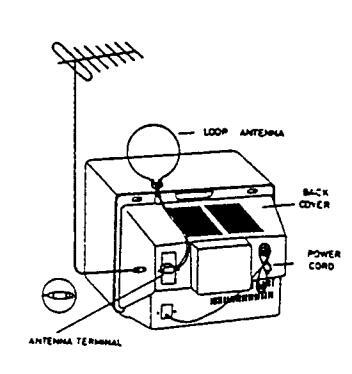
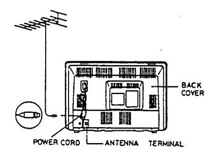
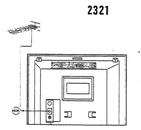
ANTENNA CONNECTIONS
LOOP ANTENNA
Under difficult reception conditions, it might be impossible to obtain good reception. In order to improve the guality of reception use an outdoor antenna.
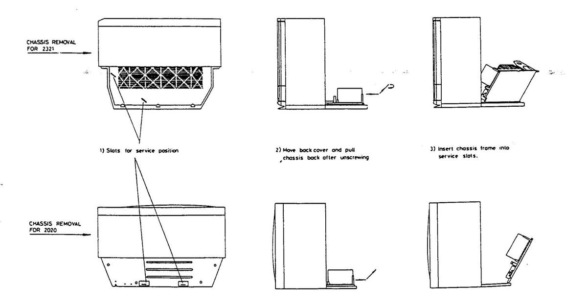
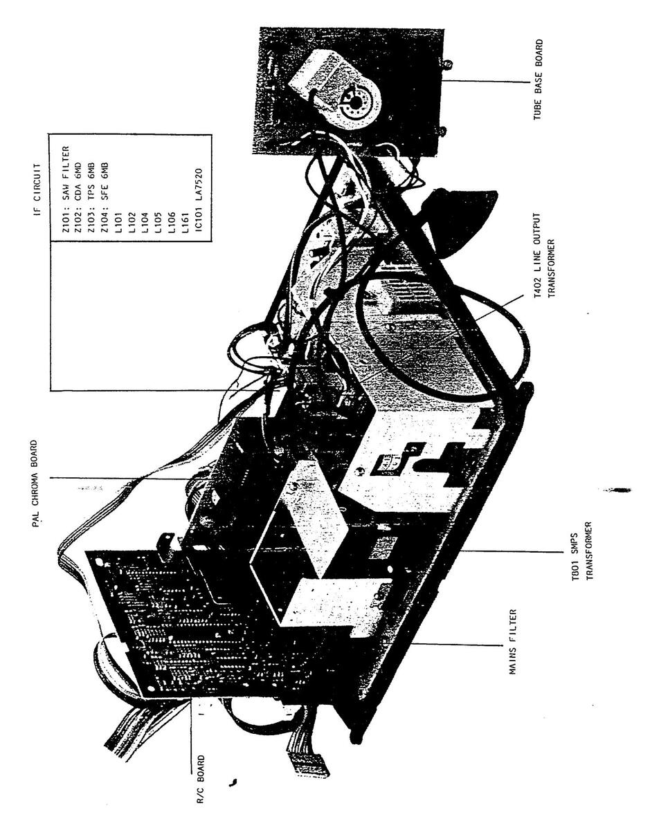
DISASSEMBLY INSTRUCTIONS
MAIN CHASSIS REMOVAL
- 1. Remove chassis retaining screws.
- 2. Grasp both sides of main chassis and pull it backward approximately 1/2 way.
- 3. Lift main chassis up and it may be removed.
CONTROL BOARD REMOVAL
1. Remove 2 screws securing the control board
CRT REMOVAL
- 1. Place the CRT on soft material against its face
- 2. Remove 4 screws fixing the CRT
.
CONTROLS LOCATION
2114
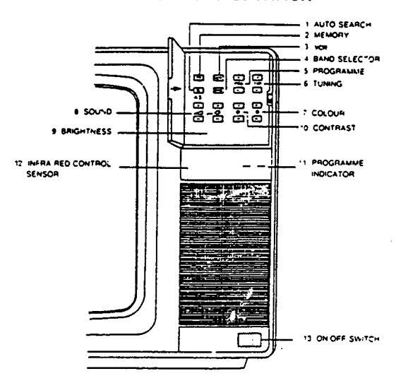
CONTROLS LOCATION
2020
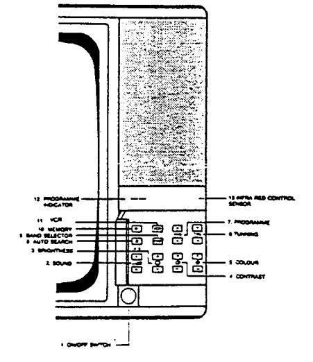
CONTROLS LOCATION
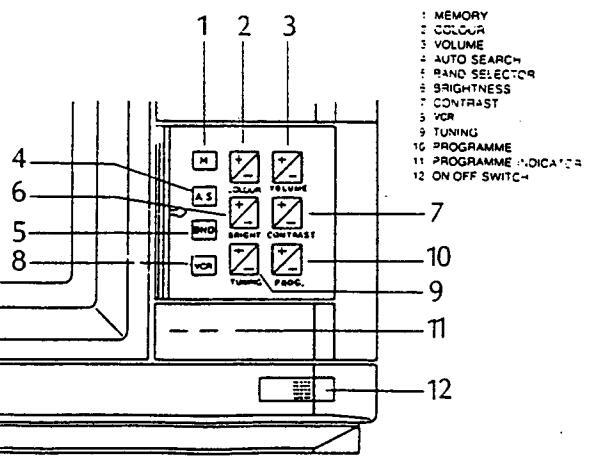
Page 8
PART LOCATION
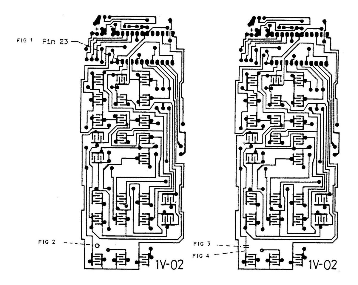
PROCEDURE TO CONVERT HAND SET INTO AN EEPROM GENERATOR
- 1. Solder a thin insulated wire to Pin 23 on IC SAA 1250 (see Fig. 1)
- 2. Run this wire through the tiny hole provided to the other side of the PCB (see Fig. 2)
- 3. Break the print between normal and number 4 control by cutting with a sharp blade (see Fig. 3)
- 4. Solder the wire to the little spot of the normal control conductive track where it has been cut (see Fig. 4)
AFTER THE ABOVE PROCEDURE NORMAL FUNCTION BUTTON WILL WORK AS SERVICE BUTTON
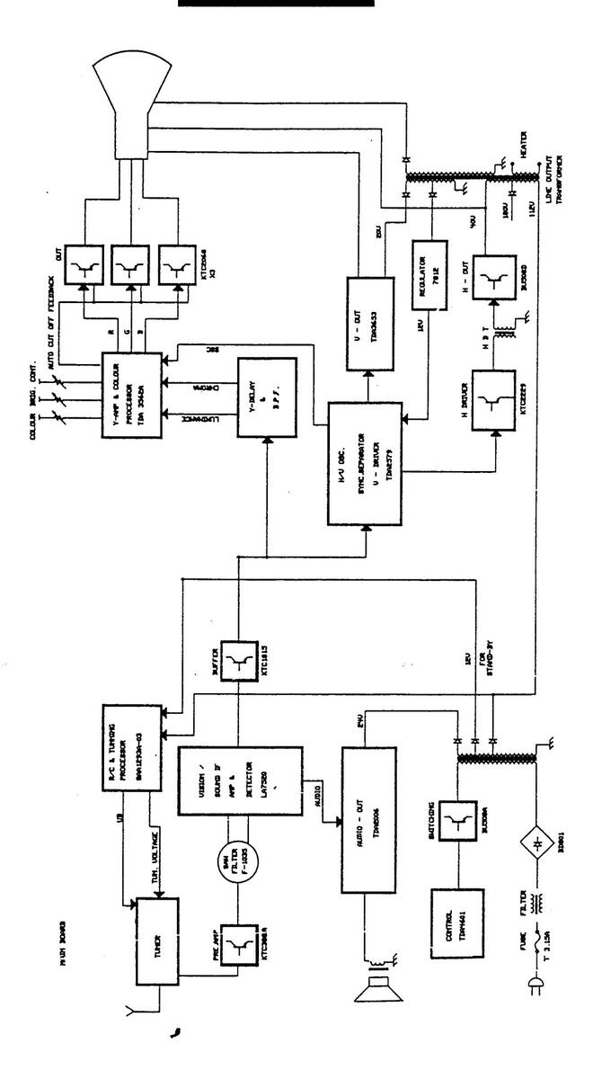
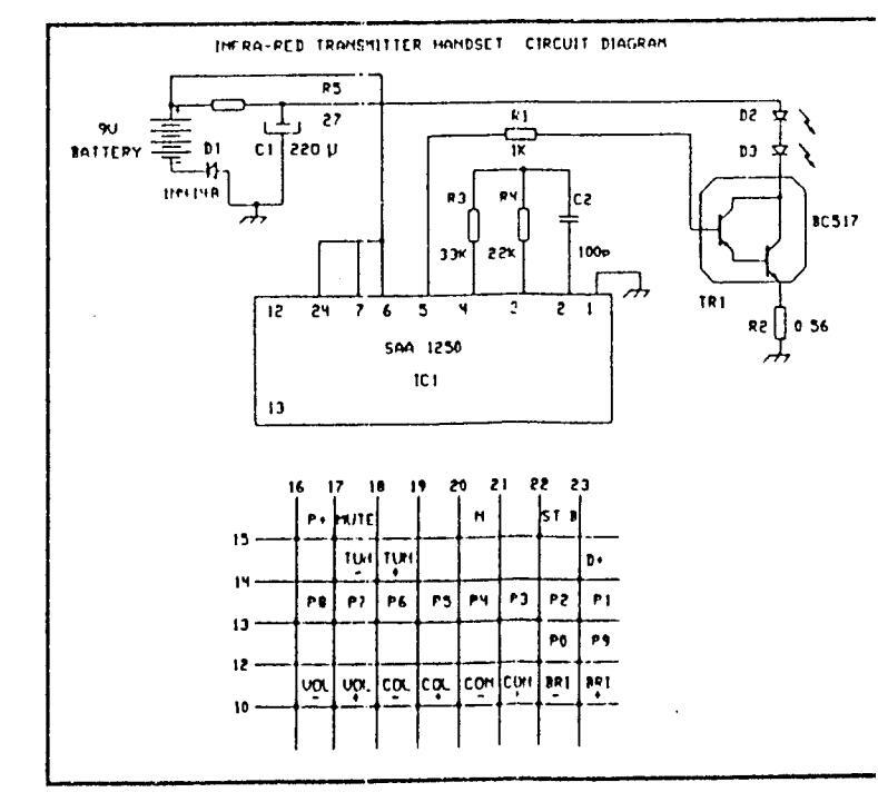
BLOCK DIAGRAM

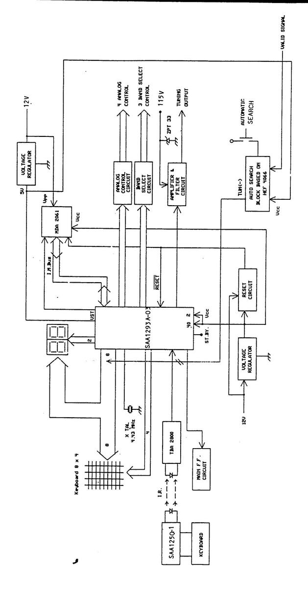
VOLTAGE SYNTHESIZED TUNING BLOCK DIAGRAM
Page 12
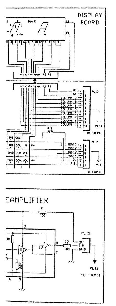
DISPLAY DIGIT
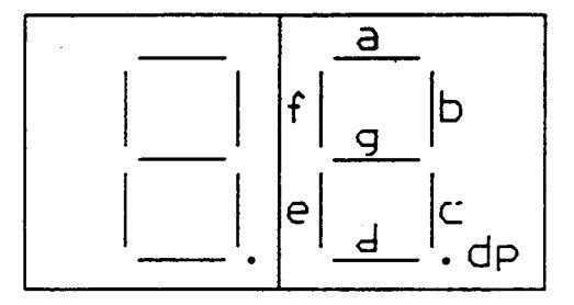
DIGIT 1
DIGIT 2
| SEGMENT | TRANSMITTER | ||
|---|---|---|---|
| 0 | 1 _ Programma Button | ||
| a | |||
| b | 2 – Programme Button | ||
| С | 3 – Programme Button | ||
| d | 4 – Programme Button | ||
| е | 5 – Programme Button | ||
| f | 6 – Programme Button | ||
| g | 7 – Programme Button | ||
| dp | 8 - Programme Button | ||
The above table shows which segments can be made on or off by using the buttons on the remote control handset.
| OPTIONS | SAA 1293-02 | SAA 1293-03 | |
|---|---|---|---|
| Option 1 | c-d-g | c-d | |
| Option 2 | b-dp | 9 * | |
| Option 3 | a-f-d-c | ||
| Option 4 | a-e |
Segments that must be "ON" with option 4 for example. a-e
ر
Page 13
Digit 1 shows the option number, Digit 2 shows the information that will be loaded. If you press the service button in succession, all four options appear one after another. Digit 2 segments can be switched "ON" or "OFF" by pressing the channel program buttons (1-8) on the remote control transmitter.
| FUNCTIONS ON REMOTE TRANSMITTER | TABLE "A" |
TABLE "B"
UHF/VHF UHF |
|
|---|---|---|---|
| D.1. D.2. | D.1 D.2. | D.1 D.2. | |
| PRESS THE SERVICE BUTTON ONCE | |||
| PRESS THE SERVICE BUTTON SECOND TIME | |||
|
OPTION 1
PRESS THE SERVICE BUTTON THIRD TIME |
|||
|
OPTION 2
PRESS THE SERVICE BUTTON FOURTH TIME |
|||
|
OPTION 3
PRESS THE SERVICE BUTTON FIFTH TIME |
|||
|
OPTION 4
PRESS THE SERVICE BUTTON SIXTH TIME |
48 | ||
| PRESS THE STAND BY BUTTON | |||
NOTES
TABLE "A"
If I.C. MDA 2061 has never been programmed or data has been lost, all of the segments in digit 2 will be illuminated.
TABLE "B"
If the segments in digit 2 are not illuminated, then the I.C. 8 (MDA2061) Database has been interrupted, and requires reprogramming by actioning the series of commands as illustrated above.
و
ADJUSTMENT INSTRUCTIONS
VISION IF ALIGNMENT
DETECTOR COIL ALIGNMENT
1. Connect test equipment to the main board as shown in Figure 1 and turn power on.
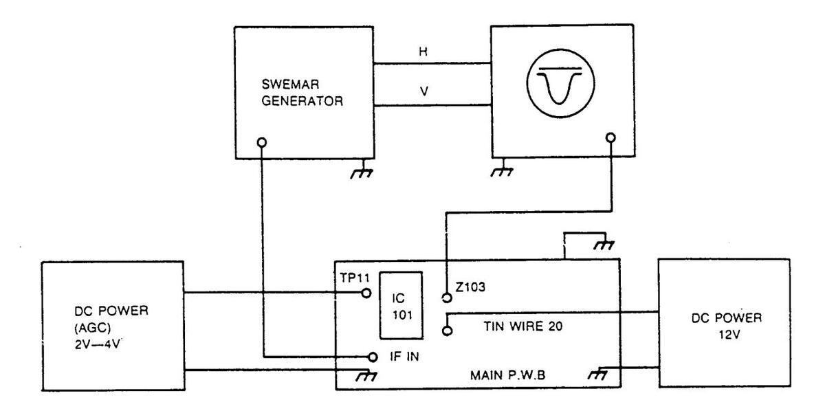
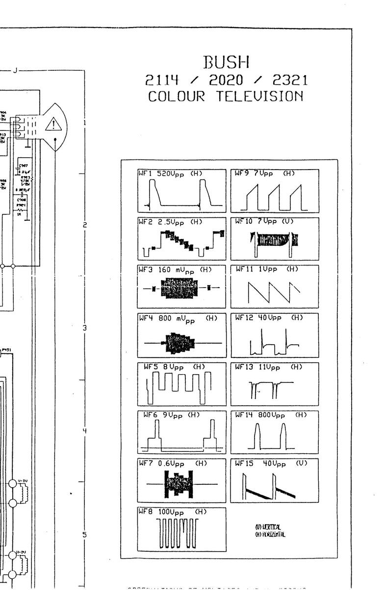
Figure 1 : Connection Diagram for VIF and AFT alignment
2. Adjust L104 main board so that the waveform is as indicated in Figure 2. Adjust, L104 so as to set the picture carrier to minimum. The adjustment should be such as not to decrease the amplitude of the whole waveform.
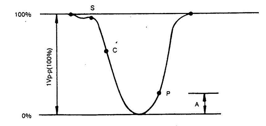
Figure 2 : L 104 Alignment Waveform
ر
3
AFT ALIGNMENT
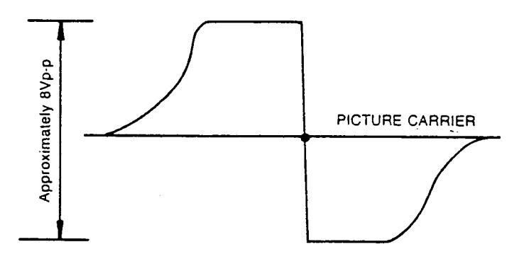
- 1. Remove the alignment scope connection from Z103 and connect to AFT pin of tuner.
- 2. Adjust L105 so that the waveform should be as shown in Figure 3.
- 3. Connect C164 after the adjustment.
DELAY AGC ALIGNMENT
- 1. Apply the standard bar signal (60 dB ± 1 dB) to the antenna terminal of the TV set.
- 2. Connect a DC voltmeter to TP14.
- 3. Adjust VR101 so that the voltmeter reads:
6.5V ± 0.1V (For the tuner TEMD5) 5.5V ± 0.1V (For the tuner TEMD1) 6.0V ± 0.1V (For the tuner TEMB1)
-
+ B (115V) ALIGNMENT (*)
- 1. Set the contrast, brightness and colour control to minimum.
- 2. Connect DVM to TP44.
- 3. Adjust VR801 so that the VDM reads 115V ± 0.1V.
ر
(*) When FBT will be changed readjust 115V DC.
HORIZONTAL SYNC. ALIGNMENT
- 1. Apply a standard colour signal (more than 60 dB) to the antenna terminal of the TV set.
- 2. Short between M (IC 401 pin 5) and N (GROUND).
- 3. Adjust VR401 so as to obtain the best synchronization in vertical and horizontal direction.
VERTICAL LINEARITY AND AMPLITUDE ALIGNMENT
- 1. Appy a standard colour signal (PM 5544 digital pattern) to the antenna input of the TV set.
- 2. Adjust VR301 so that the circle may be located at a position 5mm distance from top and bottom of the effective screen (AMPLITUDE ALIGNMENT).
- 3. Adjust VR301 so as to obtain an optimum circle (LINEARITY ALIGNMENT).
PAL MATRIX ALIGNMENT
- 1. Set the contrast, brightness and colour control to maximum.
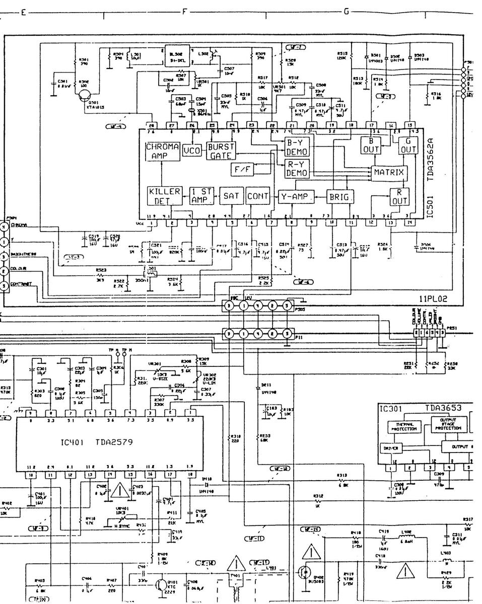
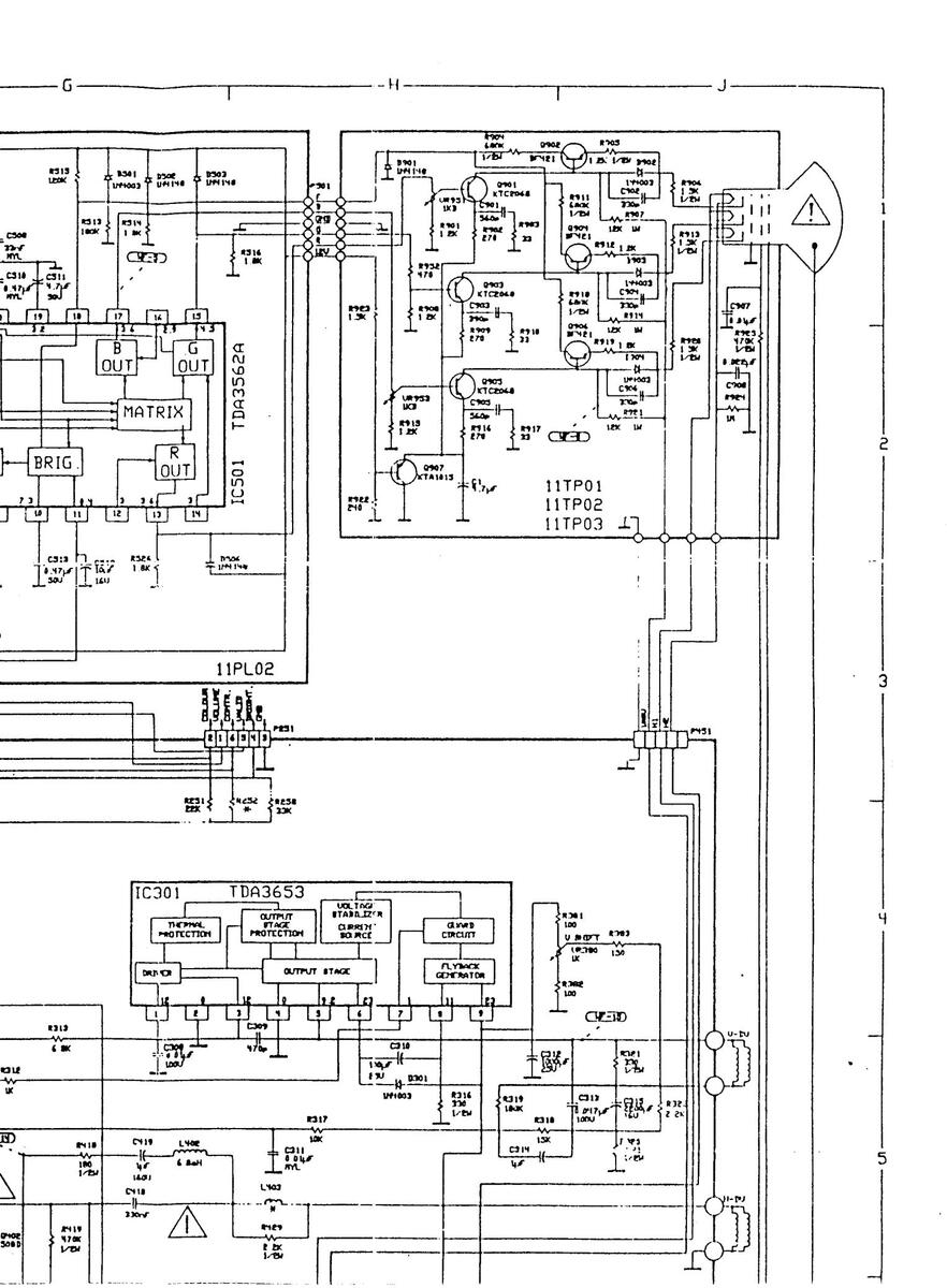
- 2. Connect the alignment oscilloscope to the base of Q905 on the CRT board or pin 17 of IC501.
- 3. Apply the standard PAL signal (PM 5544-digital pattern, more than 60 dB) to the antenna input of the TV set.
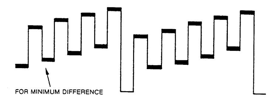
- 4. Adjust VR501 for minimum amplitude of point A and B as shown in Figure 4.
Figure 4 : Waveform of Alignment Oscilloscope
5. Change the applied signal to the standard colour bar signal.
.
6. Adjust L502 to obtain minimum difference.
Figure 5 : Oscilloscope Alignment Waveform
SCREEN VOLTAGE ALIGNMENT
(WHITE BALANCE ADJUSTMENT IN LOW AMBIENT LIGHT)
- 1. Connect a colour signal more than 60 dB to the antenna terminal of the TV set.
- 2. Set R951 and R953 on the CRT board to the mechanical centre and the COLOUR CONTROL to minimum.
- 3. ADJUST the CONTRAST and BRIGHTNESS CONTROL gradually counter-clockwise to obtain picture brightness of 40-100 LUX.
- 4. Vary the SCREEN CONTROL right and/or left and set it to the position WHERE a FLYBACK line and smear DOES NOT appear on the screen.
- 5. Set the CONTRAST and BRIGHTNESS CONTROL to minimum and check the screen condition.
WHITE BALANCE ALIGNMENT IN HIGH AMBIENT LIGHT
-
1. CONNECT a standard colour signal more than 60 dB to the antenna board of the TV set.
- 2. Set the COLOUR CONTROL to minimum and CONTRAST and BRIGHTNESS CONTROL to maximum.
- 3. Adjust R951 and R953 on the CRT board in ORDER to obtain the white screen (colour temperature : 8500°C 9500°C).
HORIZONTAL CENTRE ALIGNMENT
1. Receive a standard OFF AIR signal.
و
2. Adjust VR402 so that right HAND SIDE position of screen is equal to the left.
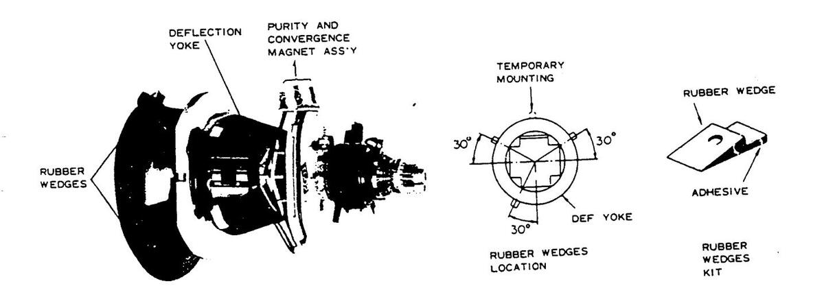
PURITY AND CONVERGENCE ADJUSTMENT
WARNING:
CONVERGENCE AND PURITY HAVE BEEN FACTORY ALIGNED. DO NOT ATTEMPT TO TAMPER WITH THESE ALIGNMENTS. HOWEVER, THE EFFECTS OF ADJACENT RECEIVER COMPONENTS OR REPLACEMENT OF PICTURE TUBE OR DEFLECTION YOKE MAY REQUIRE THE NEED TO READJUST PURITY AND CONVERGENCE. CONVERGENCE MAGNET ASSEMBLY AND RUBBER WEDGES NEED MECHANICAL POSITIONING FOLLOWING THE FIGURE 1. BEFORE ATTEMPTING ANY CONVERGENCE ADJUSTMENT THIS RECEIVER SHOULD BE OPERATED FOR AT LEAST FIFTEEN MINUTES. IF ADJUSTMENT IS REQUIRED THE ADJUSTMENTS SHOULD BE MADE IN THE FOLLOWING SEQUENCE.
COLOUR PURITY ADJUSTMENT
- 1. Demagnetize the picture tube and cabinet using a degaussing coil.
- 2. Turn the CONTRAST and BRIGHTNESS controls to maximum.
- 3. Rotate RED and BLUE BIAS controls (R557 & R559) fully clockwise. Slowly rotate GREEN BIAS control clockwise to produce a green raster.
- 4. Loosen the clamp screw holding the yoke and slide the yoke backward to provide vertical green bar (zone) in the picture screen.
- 5. Remove the rubber wedges.
- 6. Rotate and spread the tabs of the purity magnet (See Fig. 1) around the neck of the picture tube until the green bar is in the centre of the screen. At the same time, centre the raster vertically.
- 7. Move the yoke slowly forward or backward until a uniform green screen is obtained. Temporarily tighten the clamp screw of the yoke.
- 8. Check the purity of the red and blue rasters by adjusting the BIAS controls.
- 9. Obtain a white raster, referring to "WHITE BALANCE ADJUSTMENT".
- 10. Proceed with convergence adjustment.
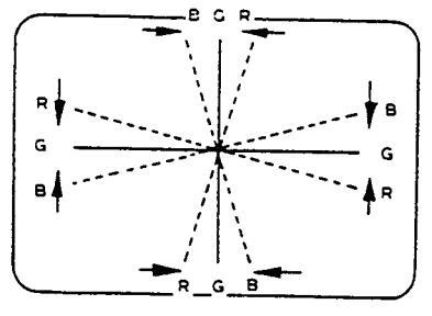
PUBITY MAGNETS
6-POLE MAGNETS
ADJUST THE ANGLE 4-POLE MAGNETS (VERTICAL LINES)
(VERTICAL LINES)
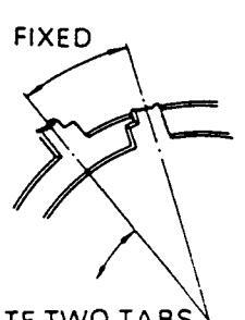
ROTATE TWO TABS
CONVERGENCE MAGNET ASSEMBLY
ADJUSTMENT OF MAGNETS
Figure 7
- 1. Apply crosshatch pattern with a colour bar signal generator.
- 2. Adjust the BRIGHTNESS and CONTRAST controls for a well defined pattern.
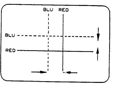
- 3. Adjust the two tabs of the 4-pole magnets to change the angle between them (See Figure 8-a) and superimpose the red and blue vertical lines in the centre area of the picture screen.
- Turn both tabs at the same time keeping their angles constant to superimpose red and blue horizontal lines at the centre of the screen (See figure 8-b).
- 5. Adjust the two tabs of 6-pole magnets to superimpose red/blue line with green one. Adjusting the angle affects the vertical lines and rotating both magnets affects the horizontal lines.
- Repeat adjustments 1,2,3 keeping in mind red, green and blue movements, because 4-pole magnets and 6-pole magnets interact and make movement complex.
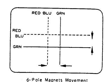
4-Pole Magnets Movement
Figure 8-a Centre Static Convergence by Convergence Magnets
Incline the Yoke up (or down)
ر
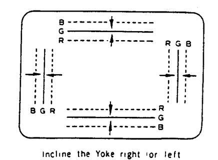
Figure 8-b Outeredge Dynamic Convergence by Deflection Yoke
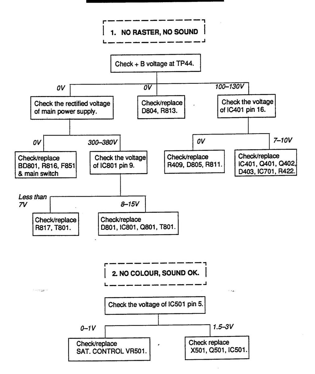
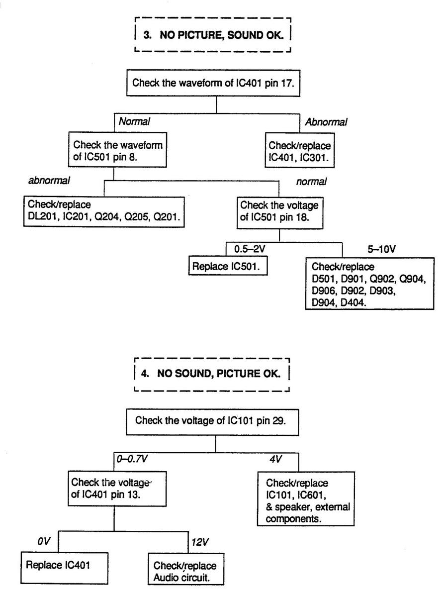
TROUBLESHOOTING CHART
Page 21
٦
Page 22
٦
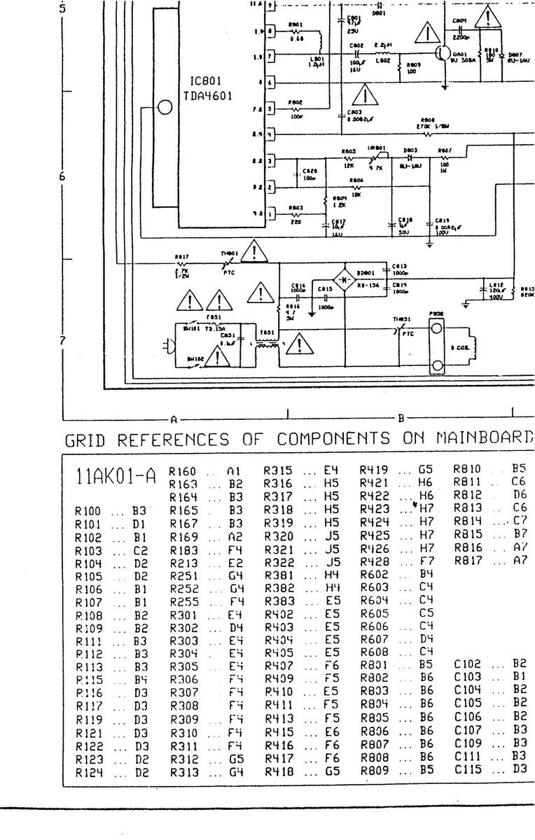
TERMINAL VIEW OF SEMICONDUCTORS
| REFERENCE NO | FIGURE |
DESCRIP-
TION |
REFERENCE NO | FIGURE |
DESCRIP-
TION |
|
|
D301.D402.D403.D404
D406.D407.D451.D501 D801.D803.D804.D805 D806.D807.D902 D903.D904 |
IN4003
RGP10J.RGP15J |
IC03
IC04 IC1701 IC2002 - 2004 - 2301 |
MDA2061
LMN324 TDA4433 LM2901 HEF4066 TBA2800 |
|||
|
D1.D2.D3.D4
D02.D11-14.D02-08 D101.D102.D201 D202.D251.D501 D503.D505.D901 |
IN4148
IS2471 |
IC05
IC2005-6 |
LM78M05CT
MC7805 TDA 16055 |
|||
| BD801 | RB-156 | IC101 | INMINISTRY'S |
KA2919
LA7520 |
||
| D01 | HP3FR2 | IC01 | TURNANA STAR | SAA 1250 | ||
|
Q401.Q902.Q904
Q906 |
ктС2229-О/Ү
ВF421 |
IC801 - 301 | TDA 4601 - 3653 | |||
|
Q01,Q161,Q201
Q203,Q204,Q205 Q501 |
E C |
KTC388A
KTA1015-O/Y KTC1815-O/Y KTC1815-Y KTC1915-Y |
IC401 | TDA2579 | ||
| Q402 | 8U508D |
IC501
IC1601 |
i mainin. |
TFK
TDA3562A M193 |
||
| Q801 | BU508A | IC601 | TDA2006 | |||
|
Q901,Q903,Q905
Q907 |
2SC2068 | IC701 | B C C E | GL7812 | ||
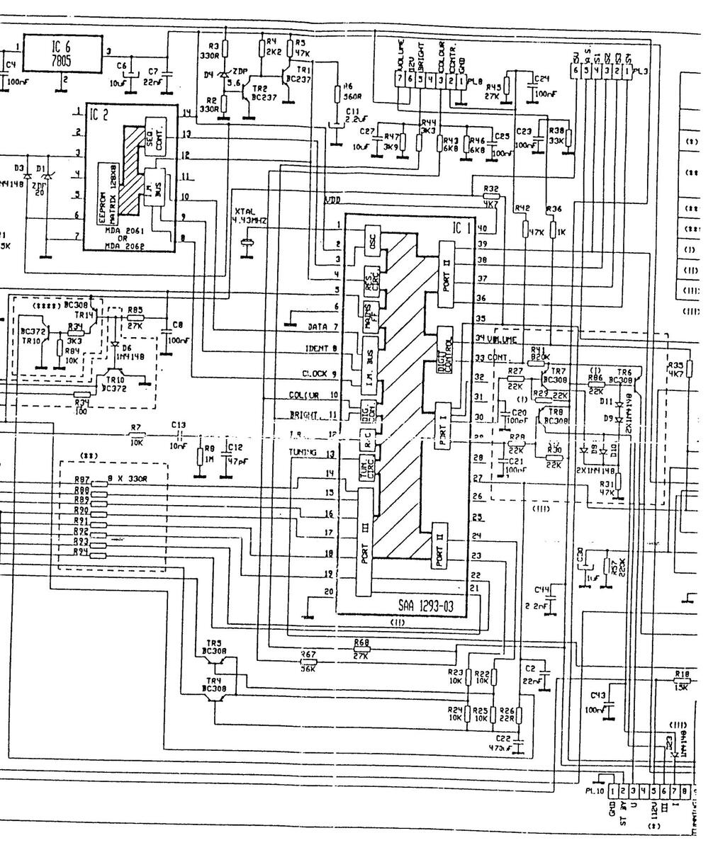
| IC 2001 | SAA 1293-03 | , | • |
ر
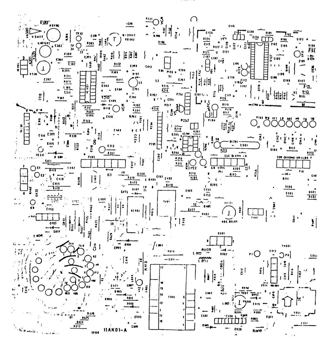
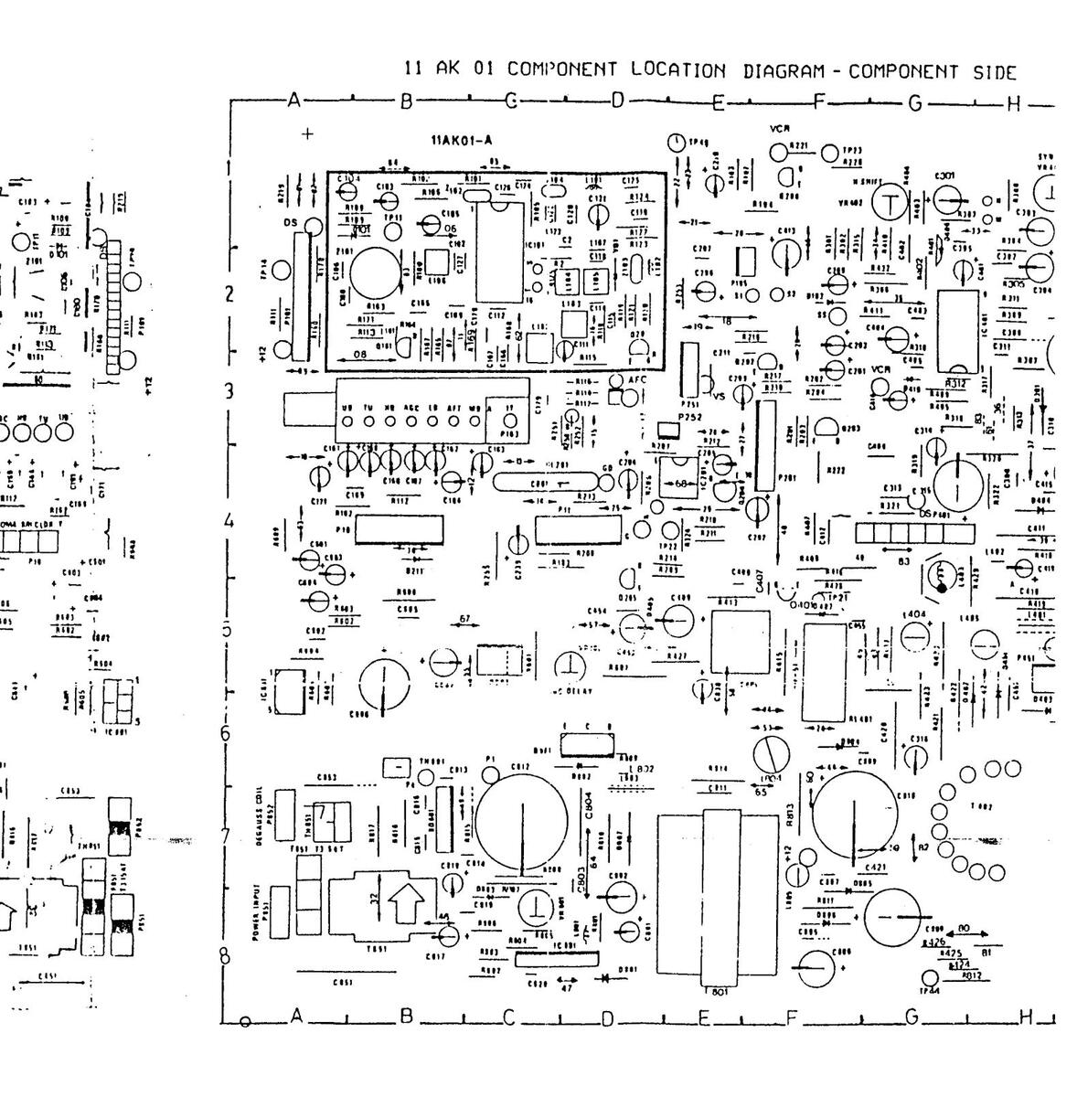
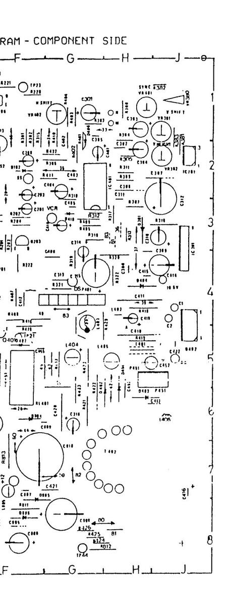
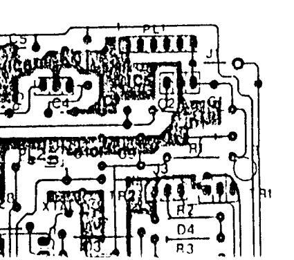
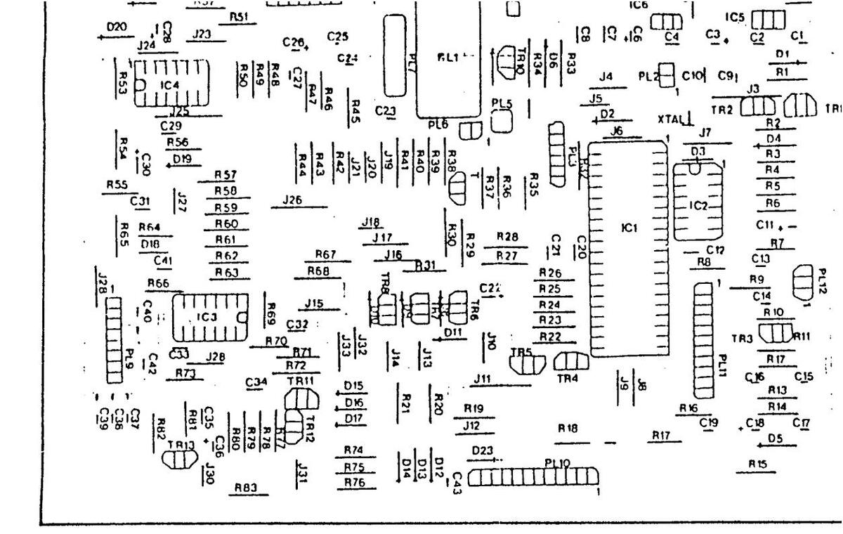
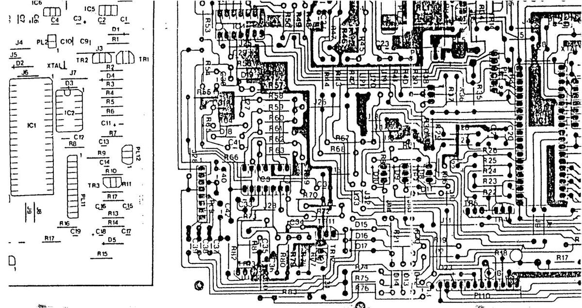
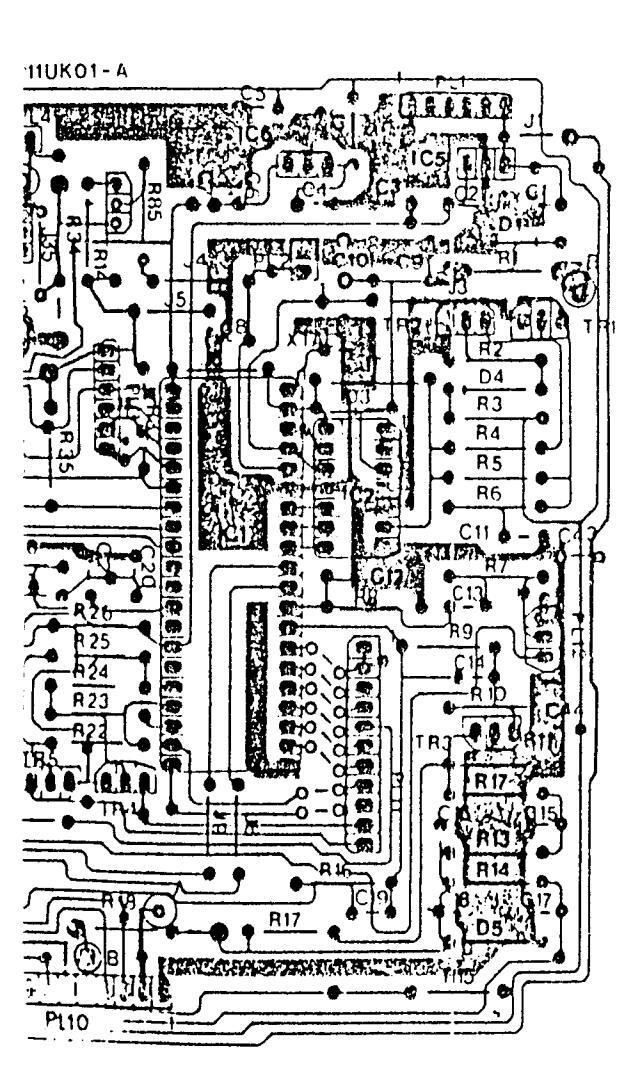
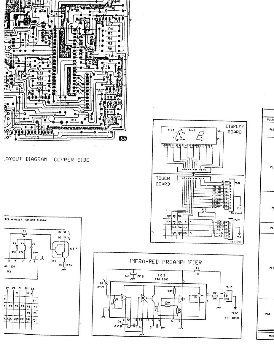
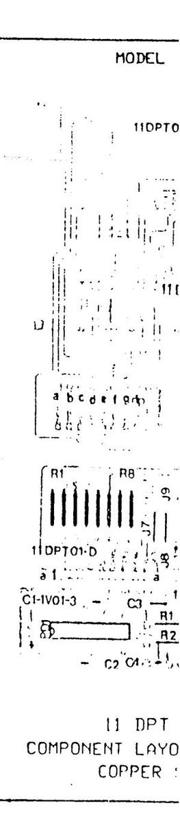
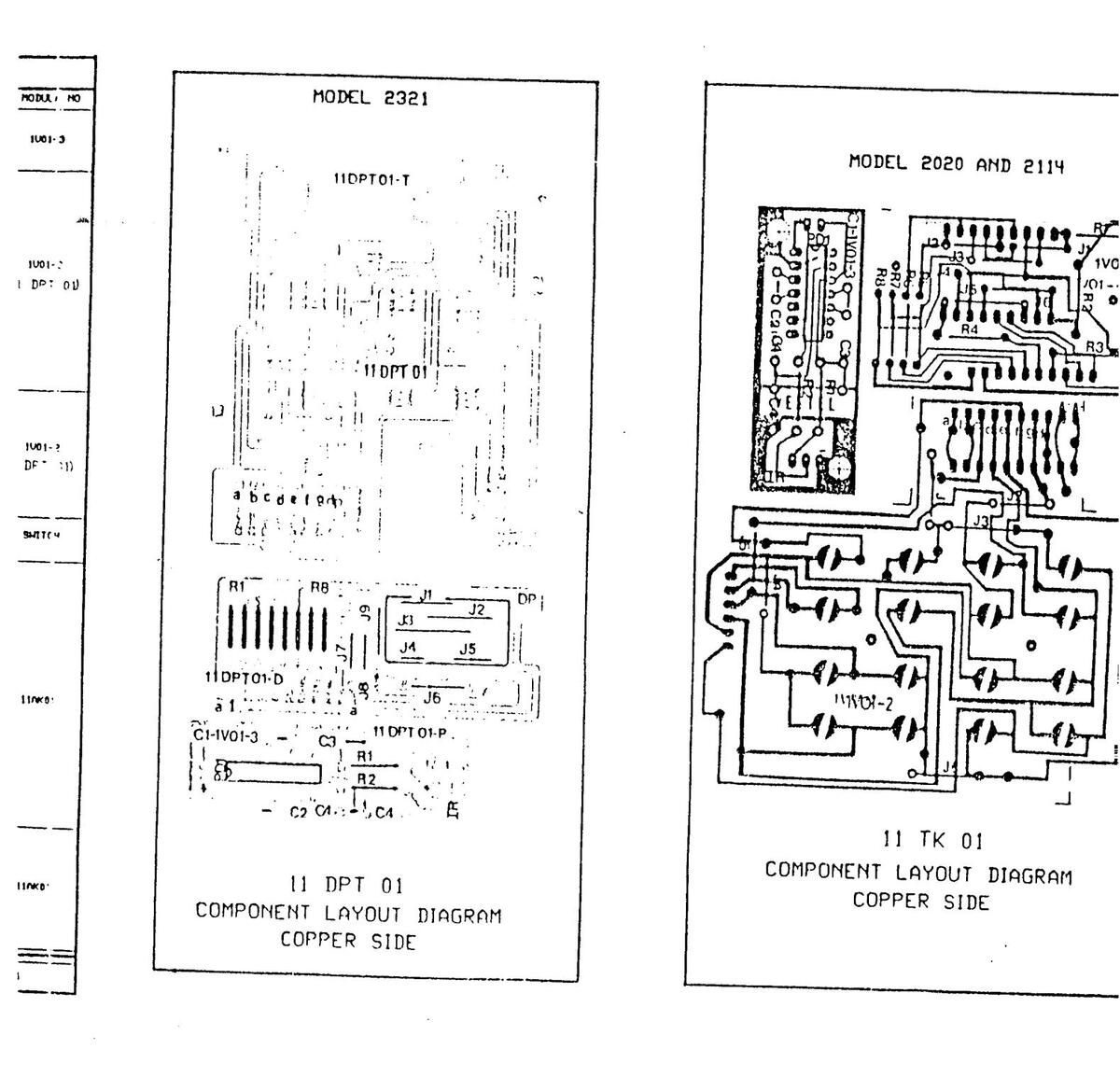
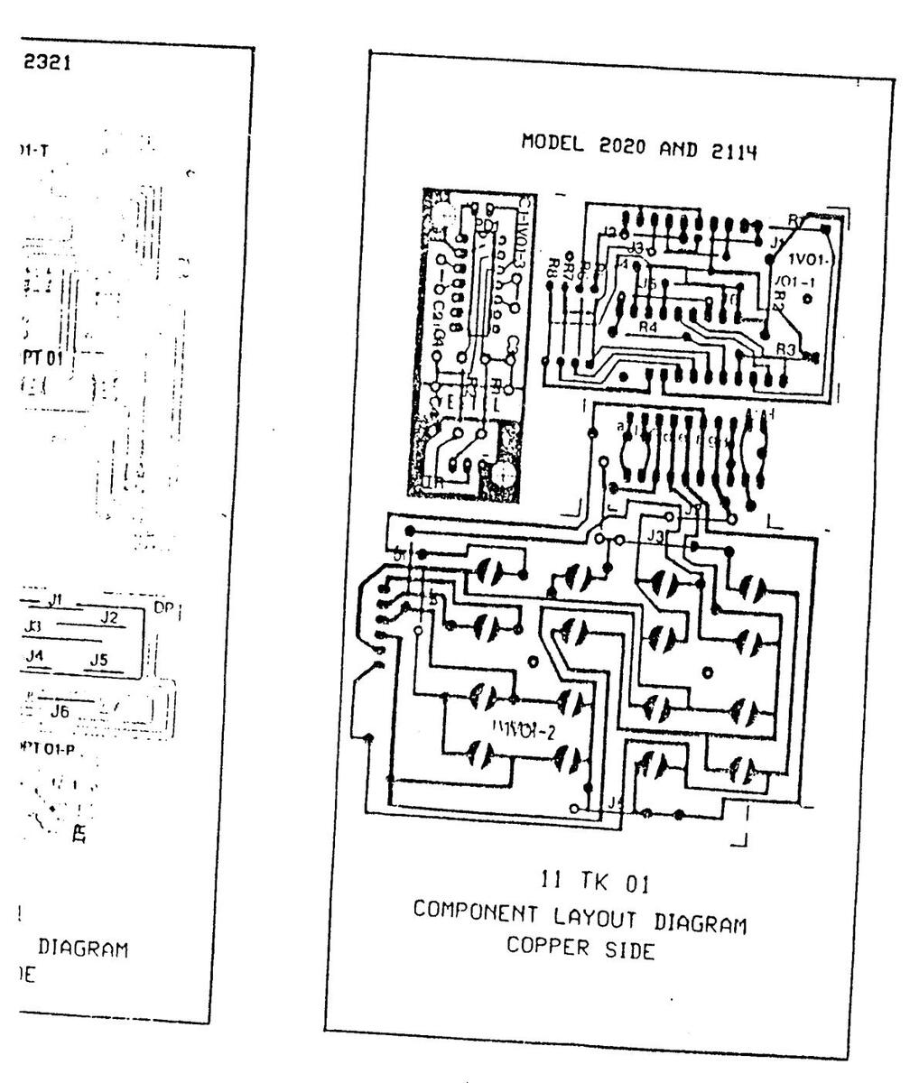
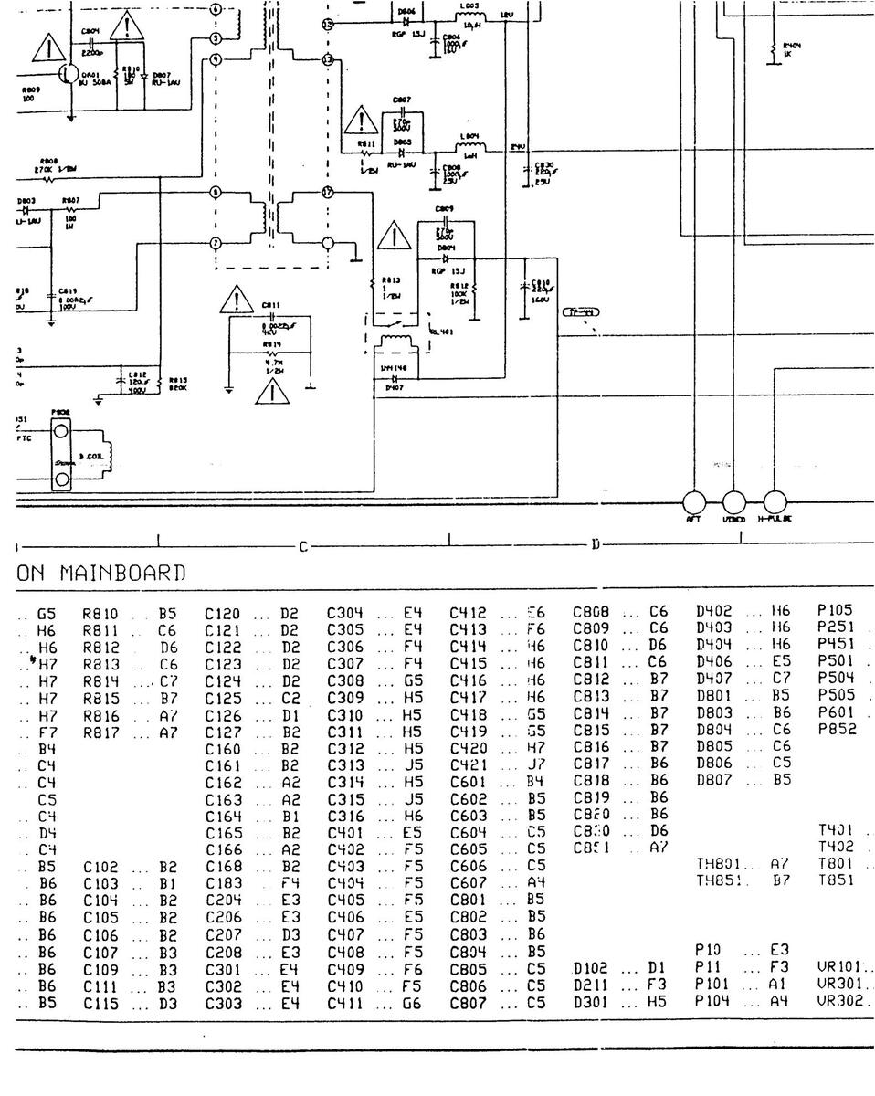
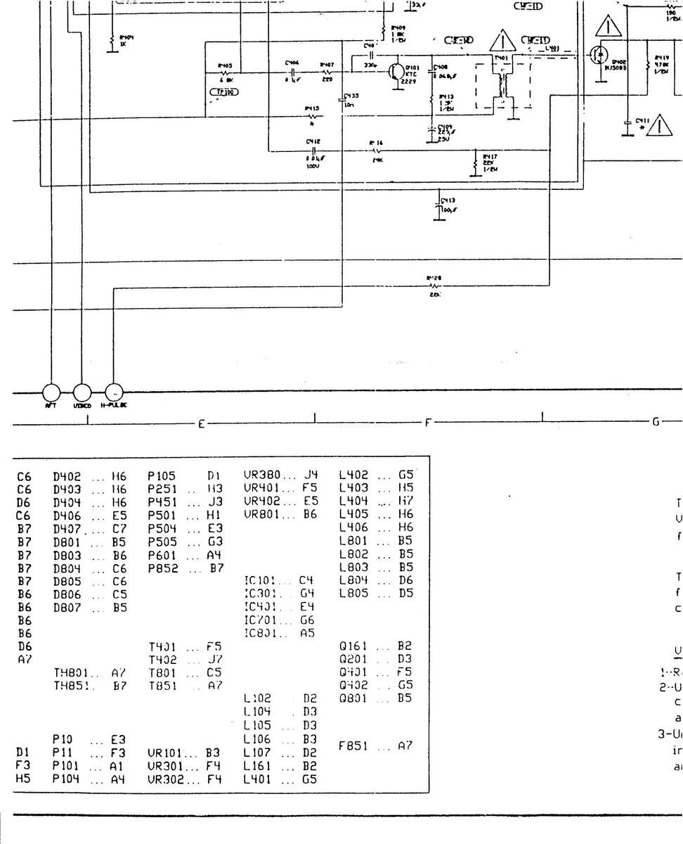
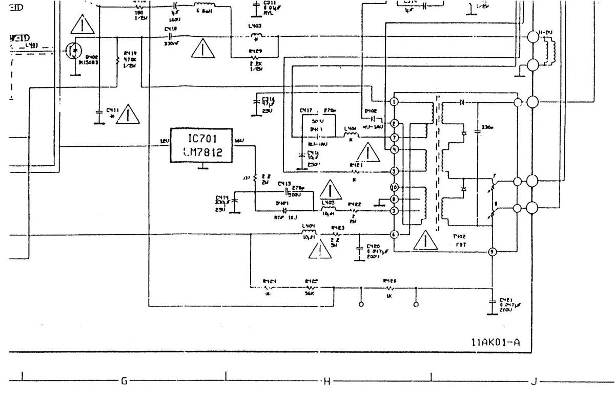
11 AK 01 COMPONENT LAYOUT DIAGRAM - COPPER SIDE
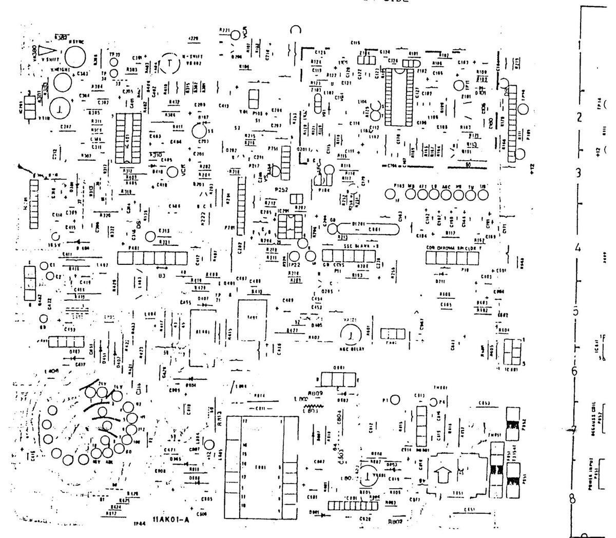
11 AK 01 COMPONENT LAYOUT DIAGRAM-COPPER SIDE
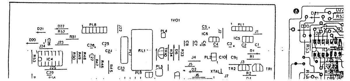
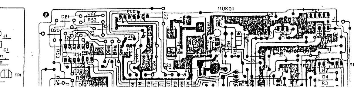
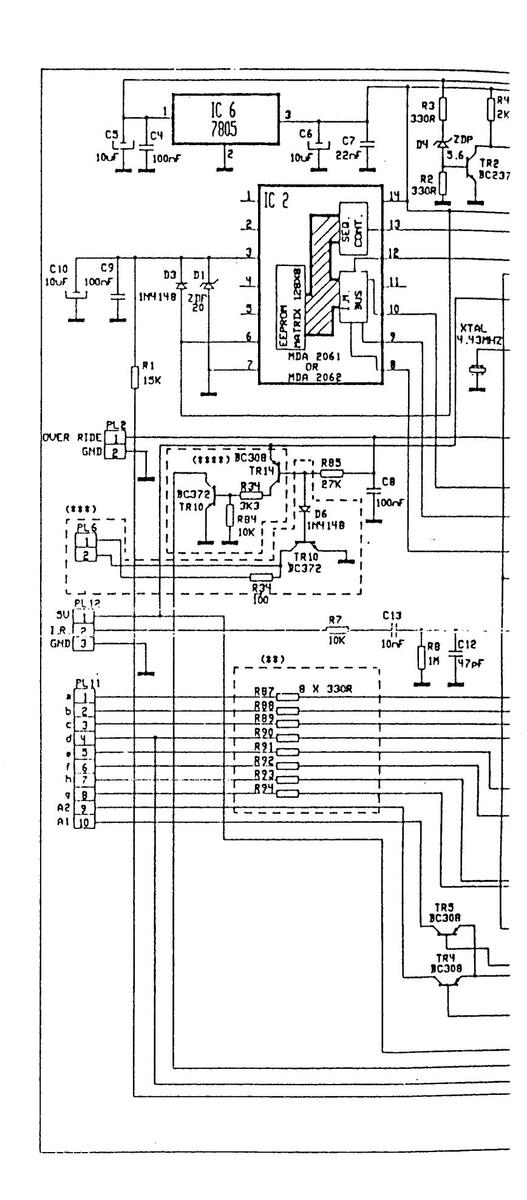
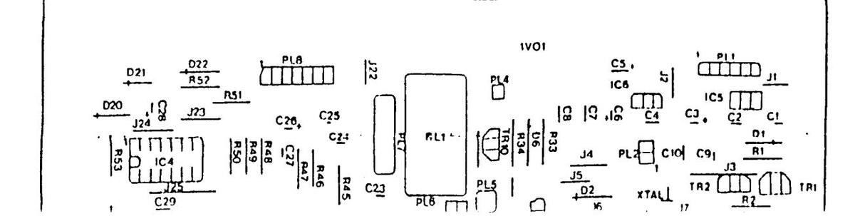
REMOTE CONTROL RECEIVER BOARDS CIRCUIT DIAGRAM
110K01A COMPONENT LAYOUT DIAGRAM COPPER SIDE
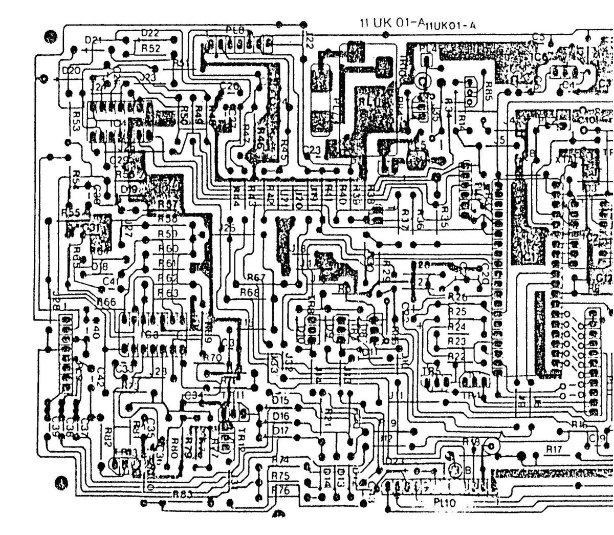
1001 COMPONENT LAYOUT DIAGRAM COPPER SIDE
AM COPPER SIDE
11UK01 COMPONENT LAYOUT DIAGRAM COPPER S
IAGRAM COPPER SIDE
2.2. A state of the second se second se second s
REMOTE CONTROL RECEIVED BO CIRCUIT DIAGRAM
REMOTE CONTROL RECEINTE BOARDS CIRCUIT DIAGRAM
and the second
The components marked with ______ conform to UDE or IEC guide lines and are essential for safe operation of the sat.
The components marked with A are required for correct operation. When replacing the components, use only the specified parts.
VALUES OF RESISTORS, CAPACITORS AND INDUCTORS
- 1-Resistances are shown in ohms; K=1000 , M=1000000 2--Unless otherwise noted in circuit diagram, all capacitor values less than 1 are expressed in µF and the values more than 1 are in pF.
- 3-Unless otherwise noted in circuit diagram, all inductor values more than 1 are expressed in mH and the values less than 1 are in µH.
OBSERVATIONS OF VOLTAGES AND WAVEFORMS
1-Uoltages read with UTUM are taken from point shown to chasis ground. Line voltage is 180-270U. 2-Voltages reading may vary ± 20 % 3-The circuit shown is only representative
4-All waveforms are taken by using a wide band oscilloscope and a low capacity probe
CAUTION
Since this is a basic circuit diagram, the values of the components and some partial connections may be changed for improvement.
| 1 | ||||
|---|---|---|---|---|
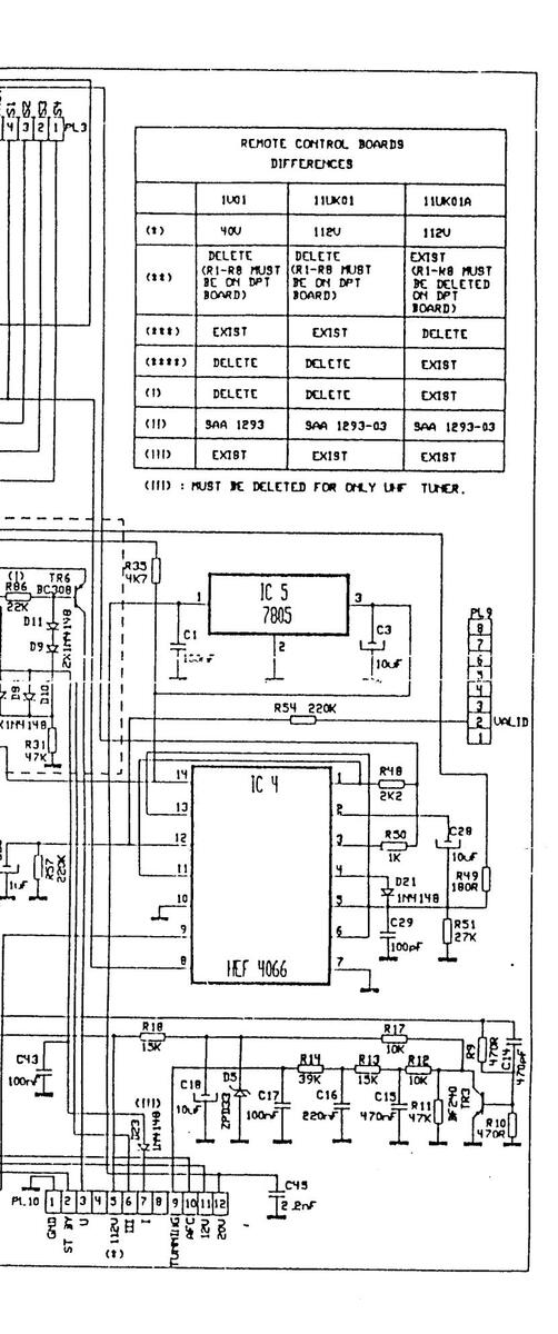
| BUSH BASIC CHASSIS (11AK01-A) COMPONENT DIFFERENCES | ||||
|
REF NO
(*) |
MODEL 2114 | MODEL 2020 | MODEL 2321 | |
| R108 | 18K | 15K | 5.6K | |
| R252 | 91K | 75K | 75K | |
| P.415 | 100R | 220R | 220R | |
| R421 | 0.47R-1/2W | 1R / 1W | 1R / 1W | |
| R424 | 43K | - 27K | 27К | |
| C411/ | F8.2 | 6.8nF | - 6.8nF | |
| 224L | 224û | 2540 | ||
| L406 | 6.8mH | Link | Link | |
| TUBE | 370 HUB22-TC02 | 510 YUB22-TC02 | A51, ISY61X03 | |
IMPORTANT: The components marked with "**", must be deleted for the "Only UHF" Tuner.
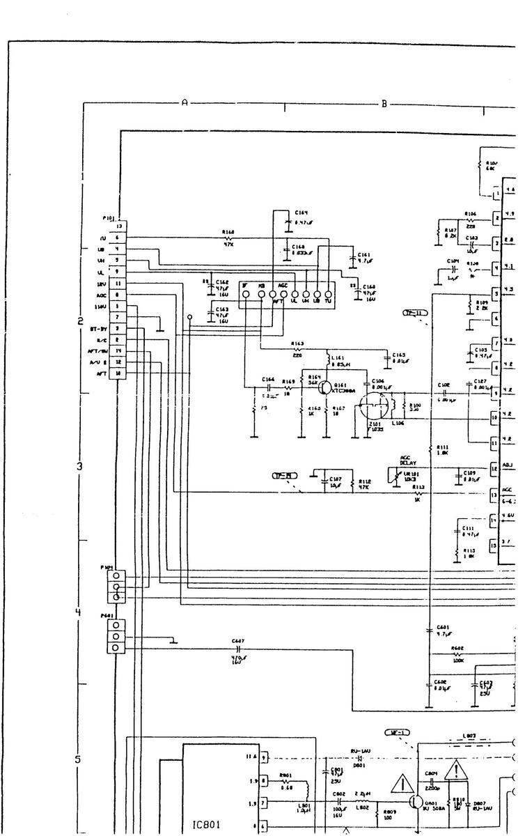
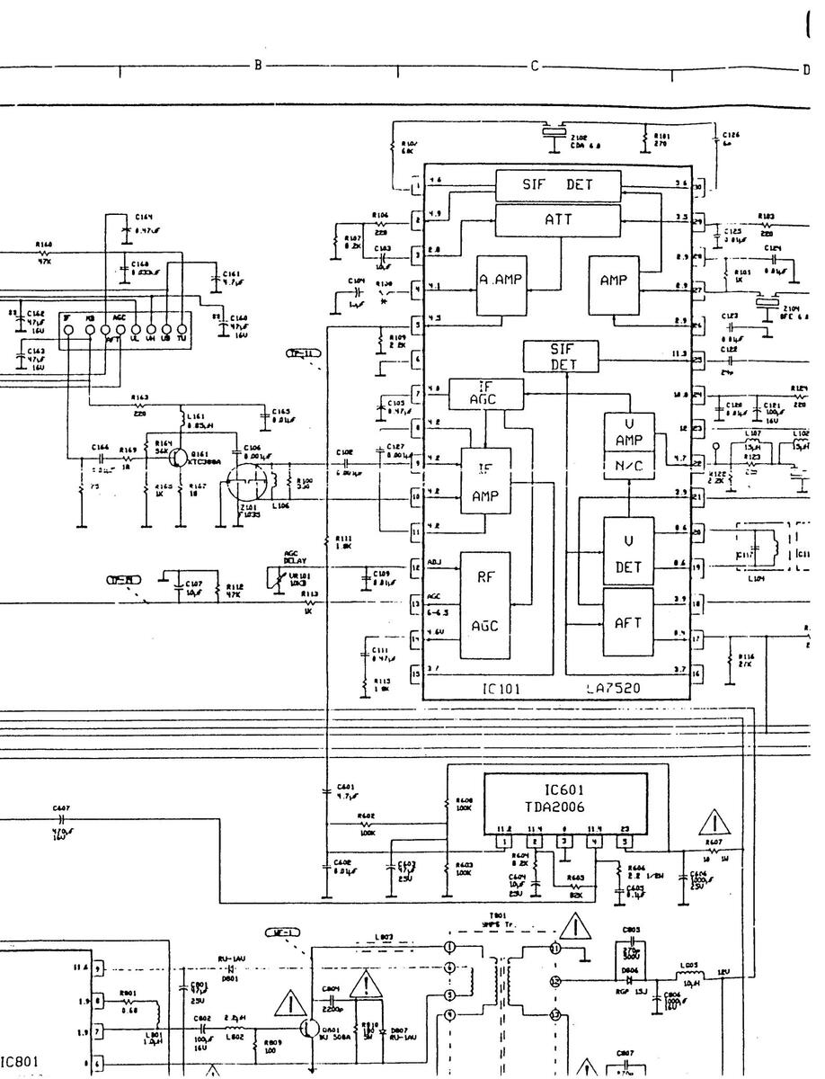
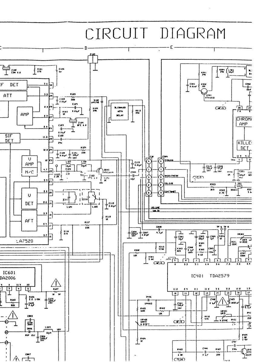
DIAGRAM


 Loading...