


AUSTN AS58C1001SF-15-IT, AS58C1001SF-15-883C, AS58C1001F-25-IT, AS58C1001F-25-883C, AS58C1001F-20-XT Datasheet
...
|
|
|
|
EEPROM |
|
|
|
Austin Semiconductor, Inc. |
|
AS58C1001 |
|||
|
|
|
|
|
||
128K x 8 EEPROM |
|
|
|
|
|
|
PIN ASSIGNMENT |
|
|||||
EEPROM Memory |
|
|||||
|
|
(Top View) |
|
|
||
AVAILABLE AS MILITARY |
|
|
|
|
||
32-Pin CFP (F & SF), 32-Pin CSOJ (DCJ) |
|
|||||
SPECIFICATIONS |
|
|||||
l SMD 5962-38267 |
RDY/BUSY\ |
1 |
3 2 |
Vcc |
|
|
l MIL-STD-883 |
A16 |
2 |
3 1 |
A15 |
|
|
|
|
A14 |
3 |
3 0 |
RES\ |
|
FEATURES |
A12 |
4 |
2 9 |
WE\ |
|
|
A7 |
5 |
2 8 |
A13 |
|
||
l High speed: 150, 200, and 250ns |
|
|||||
A6 |
6 |
2 7 |
A8 |
|
||
l Data Retention: 10 Years |
A5 |
7 |
2 6 |
A9 |
|
|
l Low power dissipation, active current (20mW/MHz (TYP)), |
A4 |
8 |
2 5 |
A11 |
|
|
standby current (100μW(MAX)) |
A3 |
9 |
2 4 |
OE\ |
|
|
A2 |
1 0 |
2 3 |
A10 |
|
||
l Single +5V (+10%) power supply |
|
|||||
A1 |
1 1 |
2 2 |
CE\ |
|
||
l Data Polling and Ready/Busy Signals |
|
|||||
A0 |
1 2 |
2 1 |
I/O 7 |
|
||
l Erase/Write Endurance (10,000 cycles in a page mode) |
I/O 0 |
1 3 |
2 0 |
I/O 6 |
|
|
l Software Data protection Algorithm |
I/O 1 |
1 4 |
1 9 |
I/O 5 |
|
|
l Data Protection Circuitry during power on/off |
I/O 2 |
1 5 |
1 8 |
I/O 4 |
|
|
Vss |
1 6 |
1 7 |
I/O 3 |
|
||
l Hardware Data Protection with RES pin |
|
|||||
|
|
|
|
|
||
|
|
|
|
|
||
l Automatic Programming: |
|
|
|
|
|
|
Automatic Page Write: 10ms (MAX) |
|
|
|
|
|
|
128 Byte page size |
|
|
|
|
|
|
GENERAL DESCRIPTION
OPTIONS |
MARKINGS |
||||
l Timing |
|
|
|
||
|
150ns access |
-15 |
|
|
|
|
200ns access |
-20 |
|
|
|
|
250ns access |
-25 |
|
|
|
l |
Packages |
|
|
|
|
|
Ceramic Flat Pack |
F |
No. 306 |
||
|
Radiation Shielded Ceramic FP* SF |
No. 305 |
|||
|
Ceramic SOJ |
DCJ |
No. 508 |
||
l |
Operating Temperature Ranges |
|
|
||
|
-Military (-55oC to +125oC) |
XT |
|||
|
-Industrial (-40oC to +85oC) |
IT |
|||
*NOTE: Package lid is connected to ground (Vss). |
|
|
|||
|
|
|
|
|
|
|
|
PIN NAME |
FUNCTION |
|
|
|
|
A0 to A16 |
Address input |
|
|
|
|
I/O0 to I/O7 |
Data input/output |
|
|
|
|
OE\ |
Output enable |
|
|
|
|
CE\ |
Chip enable |
|
|
|
|
WE\ |
Write enable |
|
|
|
|
Vcc |
Power supply |
|
|
|
|
Vss |
Ground |
|
|
|
|
RDY/Busy\ |
Ready busy |
|
|
|
|
RES\ |
Reset |
|
|
The Austin Semiconductor, Inc. AS58C1001 is a 1 Megabit CMOS Electrically Erasable Programmable Read Only Memory (EEPROM) organized as 131, 072 x 8 bits. The AS58C1001 is capable or in system electrical Byte and Page reprogrammability.
The AS58C1001 achieves high speed access, low power consumption, and a high level of reliability by employing advanced MNOS memory technology and CMOS process and circuitry technology and CMOS process and circuitry technology.
This device has a 128-Byte Page Programming function to make its erase and write operations faster. The AS58C1001 features Data Polling and a Ready/Busy signal to indicate completion of erase and programming operations.
This EEPROM provides several levels of data protection. Hardware data protection is provided with the RES pin, in addition to noise protection on the WE signal and write inhibit during power on and off. Software data protection is implemented using JEDEC Optional Standard algorithm.
The AS58C1001 is designed for high reliability in the most demanding applications. Data retention is specified for 10 years and erase/write endurance is guaranteed to a minimum of 10,000 cycles in the Page Mode.
For more products and information please visit our web site at www.austinsemiconductor.com
|
|
|
AS58C1001 |
Austin Semiconductor, Inc. reserves the right to change products or specifications without notice. |
|
Rev. 4.0 3/01 |
1 |
|
|
|
|

EEPROM
AS58C1001
Austin Semiconductor, Inc.
FUNCTIONAL BLOCK DIAGRAM
Vcc
Vss
OE\
CE\
WE\
RES\ 

A0
A6
A7
A16
High Voltage Generator |
I/O0 |
I/O7 |
Ready/Busy |
|
|
|
I/O Buffer
and
Input Latch
Control Logic and Timing
Y Gating
Y Decoder
Address
Buffer and
Latch
X Decoder |
Memory Array |
Data Latch
MODE SELECTION
MODE |
CE\ |
OE\ |
WE\ |
RES\ |
RDY/BUSY\1 |
I/O |
|
READ |
VIL |
VIL |
VIH |
VH |
High-Z |
DOUT |
|
STANDBY |
VIH |
X |
X |
X |
High-Z |
High-Z |
|
WRITE |
VIL |
VIH |
VIL |
VH |
High-Z to VOL |
DIN |
|
DESELECT |
VIL |
VIH |
VIH |
VH |
High-Z |
High-Z |
|
WRITE |
X |
X |
VIH |
X |
--- |
--- |
|
INHIBIT |
|
|
|
|
|
|
|
X |
VIL |
X |
X |
--- |
--- |
||
|
|||||||
DATA |
VIL |
VIL |
VIH |
VH |
VOL |
Data Out |
|
POLLING |
(I/O7) |
||||||
PROGRAM |
X |
X |
X |
VIL |
High-Z |
High-Z |
Notes:
1. RDY/Busy\ output has only active LOW VOL and HIGH impedance state. It can not go to HIGH (VOH) state.
|
|
|
AS58C1001 |
Austin Semiconductor, Inc. reserves the right to change products or specifications without notice. |
|
Rev. 4.0 3/01 |
2 |
|
|
|
|

EEPROM
AS58C1001
Austin Semiconductor, Inc.
FUNCTIONAL DESCRIPTION
AUTOMATIC PAGE WRITE
The Page Write feature allows 1 to 128 Bytes of data to be written into the EEPROM in a single cycle and allows the undefined data within 128 Bytes to be written corresponding to the undefined address (A0 to A6). Loading the first Byte of data, the data load window of 30μs opens for the second. In the same manner each additional Byte of data can be loaded within 30μs. In case CE\ and WE\ are kept high for 100μs after data input, the EEPROM enters erase and write automatically and only the input data can be written into the EEPROM. In Page mode the data can be written and accessed 104 times per page, and in Byte mode 103 times per Byte.
DATA\ POLLING
Data\ Polling allows the status of the EEPROM to be determined. If the EEPROM is set to Read mode during a Write cycle, and inversion of the last Byte of data to be loaded outputs from I/O, to indicate that the EEPROM is performing a Write operation.
PROGRAMMING/ERASE
The 58C1001 does NOT employ a BULK-erase function. The memory cells can be programmed ‘0’ or ‘1’. A write cycle performs the function of erase & write on every cycle with the erase being transparent to the user. The internal erase data state is considered to be ‘1’. To program the memory array with background of ALL 0’s or All 1’s, the user would program this data using the page mode write operation to program all 1024 128-byte pages.
DATA PROTECTION
To protect the data during operation and power on/off, the AS58C1001 has:
1. Data protection against Noise on Control Pins (CE\, OE\, WE\) during Operation. During readout or standby, noise on the control pins may act as a trigger and turn the EEPROM to programming mode by mistake. To prevent this phenomenon, the AS58C1001 has a noise cancellation function that cuts noise if its width is 20ns or less in programming mode. Be careful not to allow noise of a width of more than 20ns on the control pins.
WRITE PROTECTION
(1)Noise protection: Noise on a write cycle will not act as a trigger with a WE\ pulse of less than 20ns.
(2)Write inhibit: Holding OE\ low, WE\ high or CE\
high, inhibits a write cycle during power on/off.
WE\ AND CE\ PIN OPERATION
During a write cycle, addresses are latched by the falling edge of WE\ or CE\, and data is latched by the rising edge of WE\ or CE\.
WRITE/ERASE ENDURANCE AND DATA RETENTION
The endurance with page programming is 104 cycles (1% cumulative failure rate) and the data retention time is more than 10 years when a device is programmed less than 104 cycles.
RDY/Busy\ SIGNAL
RDY/Busy\ signal also allows status of the EEPROM to be determined. The RDY/Busy\ signal has high impedance except in write cycle and is lowered to VOL after the first write signal. At the end of the write cycle, the RDY/Busy\ signal changes state to high impedance. This allows many 58C1001 devices RDY/Busy\ signal lines to be wired-OR together.
|
|
|
AS58C1001 |
Austin Semiconductor, Inc. reserves the right to change products or specifications without notice. |
|
Rev. 4.0 3/01 |
3 |
|
|
|
|
EEPROM
AS58C1001
Austin Semiconductor, Inc.
(EXAMPLE)
Vcc
|
RES\ |
|
|
|
|
|
|
|
|
|
|
|
|
|
|
|
|
|
|
|
|
|
|
|
|
|
|
|
|
|
|
|
|
*unprogrammable |
*unprogrammable |
||||||||
|
|
|
|
|
|
|
|
|
|
|
FUNCTIONAL DESCRIPTION (continued) |
|
|
|
|
Write Data |
|||||
|
|
|
|
|
Write Address (Normal Data Input) |
|||||
DATA PROTECTION (continued) |
|
|
|
|
|
|
||||
2. Data protection at Vcc on/off.
When RES\ is low, the EEPROM cannot be erased and programmed. Therefore, data can be protected by keeping RES\ low when Vcc is switched. RES\ should be high during programming because it does not provide a latch function. When Vcc is turned on or off, noise on the control pins generated by external circuits (CPU, etc.) may turn the EEPROM to programming mode by mistake. To prevent this unintentional programming, the EEPROM must be kept in an unprogrammable, standby or readout state by using a CPU reset signal to RES\ pin.
In addition, when RES\ is kept high at Vcc on/off timing, the input level of control pins (CE\, OE\, WE\) must be held as CE\=Vcc or OE\=LOW or WE\=Vcc level.
5555 |
AA |
2AAA |
55 |
5555 |
A0 |
The Software data protection mode can be cancelled by inputting the following 6 Bytes. This changes the AS58C1001 to the Non-Protection mode, for normal operation.
Address |
Data |
3. Software Data Protection
To protect against unintentional programming caused by noise generated by external circuits, AS58C1001 has a Software data protection function. To initate Software data protection mode, 3 bytes of data must be input, followed by a dummy write cycle of any address and any data byte. This exact sequence switches the device into protection mode. This 4th cycle during write is required to initiate the SDP and physically writes the address and data. While in SDP the entire array is protected in which writes can only occur if the exact SDP sequence is re-executed or the unprotect sequence
5555 |
AA |
2AAA |
55 |
5555 |
80 |
5555 |
AA |
2AAA |
55 |
is executed. |
20 |
5555 |
|
|
|
AS58C1001 |
Austin Semiconductor, Inc. reserves the right to change products or specifications without notice. |
|
Rev. 4.0 3/01 |
4 |
|
|
|
|

EEPROM
AS58C1001
Austin Semiconductor, Inc.
ABSOLUTEMAXIMUMRATINGS* |
|
Voltage on Vcc Supply Relative to Vss................ |
-0.5V to +7.0V1 |
Voltage on any pin Relative to Vss....................... |
-0.6V to +7.0V1 |
Storage Temperature ............................................ |
-65°C to +150°C |
Operating Temperature Range............................. |
-55oC to +125oC |
Soldering Temperature Range............................................... |
260oC |
Maximum Junction Temperature**.................................... |
+150°C |
Power Dissipation................................................................... |
1.0W |
*Stresses greater than those listed under "Absolute Maximum Ratings" may cause permanent damage to the device. This is a stress rating only and functional operation of the device at these or any other conditions above those indicated in the operation section of this specification is not implied. Exposure to absolute maximum rating conditions for extended periods may affect reliability.
** Junction temperature depends upon package type, cycle time, loading, ambient temperature and airflow.
ELECTRICAL CHARACTERISTICS AND RECOMMENDED DC OPERATING CONDITIONS
(-55oC < TA < 125oC; Vcc = 5V +10%)
PARAMETER |
CONDITION |
SYMBOL |
MIN |
MAX |
UNITS |
NOTES |
Input High (Logic 1) Voltage |
|
VIH |
2.2 |
VCC + 0.3V |
V |
9 |
Input Low (Logic 0) Voltage3 |
|
VIL |
-0.3 |
0.8 |
V |
2 |
Input Voltage (RES\ Pin) |
|
VH |
Vcc-0.5 |
VCC +1.0 |
V |
|
Input Leakage Current4 |
OV < VIN < Vcc |
ILI |
-2 |
2 |
μΑ |
4 |
Output Leakage Current |
Output(s) disabled, OV < VOUT < Vcc |
ILO |
-2 |
2 |
μΑ |
|
Output High Voltage |
IOH = -400 μA |
VOH |
2.4 |
|
V |
|
Output Low Voltage |
IOL = 2.1 mA |
VOL |
|
0.4 |
V |
|
|
|
|
|
MAX |
|
|
|
PARAMETER |
CONDITIONS |
SYM |
-15 |
-20 |
-25 |
UNITS |
NOTES |
|
IOUT=OmA, Vcc = 5.5V |
|
20 |
20 |
20 |
|
|
|
Cycle=1μS, Duty=100% |
|
|
|
|||
Power Supply Current: |
|
|
|
|
|
|
|
|
ICC3 |
|
|
|
mA |
|
|
Operating |
IOUT=OmA, Vcc = 5.5V |
65 |
55 |
50 |
|
||
|
|
|
|
||||
|
Cycle=MIN, Duty=100% |
|
|
|
|
|
|
|
|
|
|
|
|
|
|
|
CE\=Vcc, Vcc = 5.5V |
ICC1 |
350 |
350 |
350 |
μA |
|
Power Supply Current: |
|
|
|
|
|
|
|
Standby |
|
|
|
|
|
|
|
CE\=VIH, Vcc = 5.5V |
ICC2 |
3 |
3 |
3 |
mA |
|
|
|
|
||||||
|
|
|
|
|
|
|
|
CAPACITANCE
PARAMETER |
CONDITIONS |
SYMBOL |
MAX |
UNITS |
NOTES |
Input Capacitance |
TA = 25oC, f = 1MHz |
CIN |
6 |
pF |
|
Output Capactiance |
VIN = 0 |
Co |
12 |
pF |
|
|
|
||||
|
|
|
|
|
|
|
|
|
AS58C1001 |
Austin Semiconductor, Inc. reserves the right to change products or specifications without notice. |
|
Rev. 4.0 3/01 |
5 |
|
|
|
|

EEPROM
AS58C1001
Austin Semiconductor, Inc.
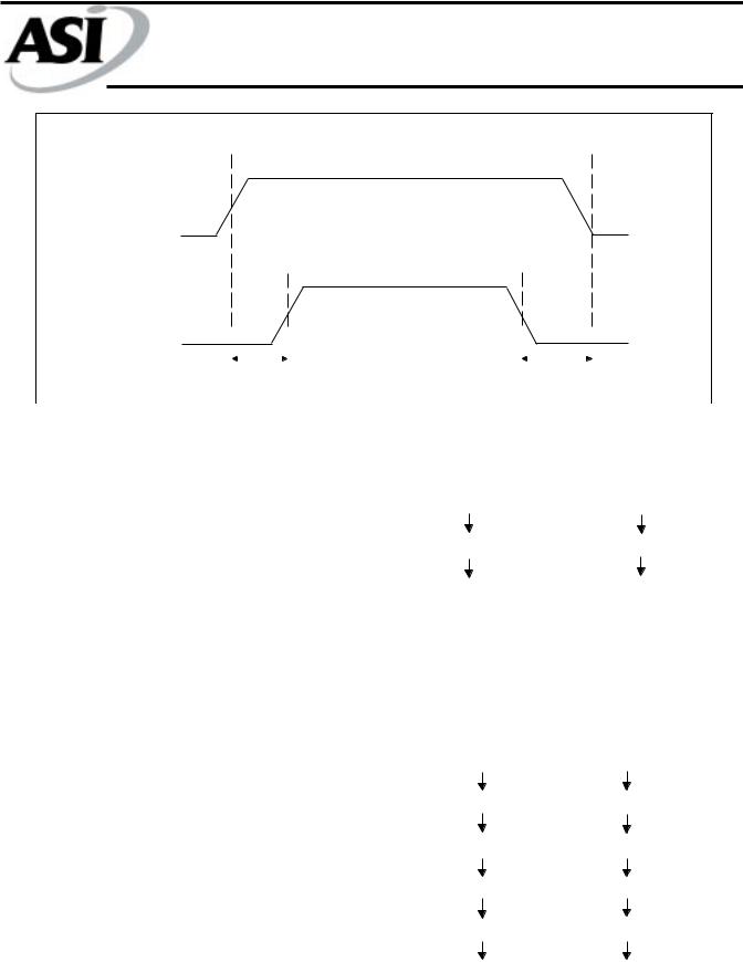
AC ELECTRICAL CHARACTERISTICS FOR READ OPERATION
(-55oC < TC < 125oC; Vcc = 5V +10%)
Test Conditions
l Input Pulse Levels: |
|
0.0V to 3.0V |
|
|
|
|
|
|
|
|
|
|
l Input rise and fall times: |
|
< 20ns |
|
|
|
|
|
|
|
|
|
|
l Output Load: |
|
1 TTL Gate +100pF (including scope and jig) |
|
|
|
|
|
|
|
|||
l Reference levels for measuring timing: |
1.5V,1.5V |
|
|
|
|
|
|
|
|
|
|
|
|
|
|
|
|
|
|
|
|
|
|
|
|
|
|
|
|
|
|
|
|
|
|
|||
|
|
|
|
|
|
|
|
|
||||
|
|
|
|
|
|
|
|
|
|
|
||
|
|
|
|
|
|
|
|
|
|
|
|
|
|
|
|
|
|
|
|
|
|
|
|
|
|
|
|
|
|
|
|
|
|
|
|
|
|
|
|
|
|
|
|
|
|
|
|
|
|
|
|
! ! " |
|
|
|
|
|
|
|
|
|
|
|
|
|
|
|
|
|
|
|
|
|
|
|
|
|
& ! " ) |
|
|
|
|
|
|
|
|
|
|
|
|
|
|
|
# |
|
|
# |
|
|
# |
|
||
|
|
|
||||||||||
$% ! & ' |
|
|
|
|
|
|
|
|
|
|
|
|
|
|
|
|
|
|
|
|
|
|
|
|
|
AC ELECTRICAL CHARACTERISTICS FOR SOFTWARE DATA PROTECTION CYCLE OPERATION
PARAMETER |
SYMBOL |
MIN |
MAX |
UNITS |
Byte Load Cycle Time |
tBLC |
0.55 |
30 |
μS |
Write Cycle Time |
tWC |
10 |
--- |
mS |
AC ELECTRICAL CHARACTERISTICS FOR DATA\ POLLING OPERATION
PARAMETER |
SYMBOL |
MIN |
MAX |
UNITS |
Output Enable Hold Time |
tOEH |
0 |
--- |
ns |
Output Enable to Write Setup Time |
tOES |
0 |
--- |
ns |
Write Start Time |
tDW |
150 |
--- |
ns |
Write Cycle Time |
tWC |
--- |
10 |
ms |
|
|
|
AS58C1001 |
Austin Semiconductor, Inc. reserves the right to change products or specifications without notice. |
|
Rev. 4.0 3/01 |
6 |
|
|
|
|
 Loading...