


 Loading...
ATMEL TS68C429AVR, TS68C429AVF, TS68C429AMRB-C, TS68C429AMR, TS68C429AMFB-C Datasheet
...Features
•8 Independent Receivers (Rx)
•3 Independent Transmitters (Tx)
•Full TS68K Family Microprocessor Interface Compatibility
•16-bit Data-bus
•ARINC 429 Interface: “1” and “0” Lines, RZ Code
•Support all ARINC 429 Data Rate Transfer and up to 2.5 Mbit/s
•Multi Label Capability
•Parity Control: Odd, Even, No Parity, Interrupt Capability
•Independent Programmable Frequency for Rx and Tx Channels
•8 Messages FIFO per Tx Channel
•Independent Interrupt Request Line for Rx and Tx Functions
•Vectored Interrupts
•Daisy Chain Capability
•Direct Addressing of all Registers
•Test Modes Capability
•20 MHz Operating Frequency
•Self-test Capability for Receiver Label Memories and Transmit FiFO
•Low Power: 400 mW
Description
The TS68C429A is an ARINC 429 controller. It is an enhanced version of the EF 4442 and it is designed to be connected to the new 16or 32-bit microprocessors, especially these of the Atmel TS68K family.
Screening
•MIL-STD-883, class B
•DESC Drawing 5962-955180
•Atmel Standards
Application Note
•A detailed application note is available “AN 68C429A” on request.
R suffix |
F suffix |
|||
PGA 84 |
CQFP 132 |
|||
Ceramic Pin Grid Array |
Ceramic Quad Flat Pack |
|||
|
|
|
|
|
|
|
|
|
|
|
|
|
|
|
CMOS ARINC 429 Multichannel Receiver/ Transmitter (MRT)
TS68C429A
Rev. 2120A–HIREL–08/02
1

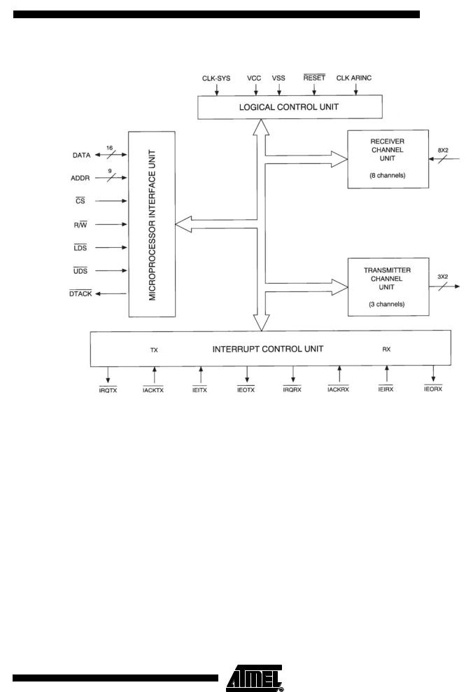
Hardware Overview The TS68C429A is a high performance ARINC 429 controller designed to interface primary to the Atmel TS68K family microprocessor in a straight forward fashion (see “Application Notes” on page 33). It can be connected to any TS68K processor family with an asynchronous bus with some additional logic in some cases.
As shown in Figure 1, the TS68C429A is divided into five main blocks, the microprocessor interface unit (MIU), the logical control unit (LCU), the interrupt control unit (ICU), the receiver channel unit (RCU) and the transmitter channel unit (TCU).
•The MIU handles the interface protocol of the host processor. Through this unit, the host sees the TS68C429A as a set of registers.
•The LCU controls the internal data flow and initializes the TS68C429A.
•The ICU manages one interrupt line for the RCU and one for the TCU. Each of these two parts has a daisy chain capability. All channels have a dedicated vectored interrupt answer. Receiver channels priority is programmable.
•The RCU is composed of 8 ARINC receiver channels made of:
–a serial to parallel converter to translate the two serial signals (the “1” and “0” in RZ code) into two 16-bit words,
–a memory to store the valid labels,
–a control logic to check the validity of the received message,
–a buffer to keep the last valid received message.
•The TCU is composed of three ARINC transmitter channels made of:
–a parallel to serial converter to translate the messages into two serial signals (the “1” and “0” in RZ code),
–a FIFO memory to store eight 32-bit ARINC messages,
–a control logic to synchronize the message transmitter (parity, gap, speed, etc.).
•Test facility: Rx inputs can be internally connected to TX3 output.
•Self-test facility: The receiver control label matrix and transmitter FIFO can be tested. This self-test can be used to verify the integrity of the TS68C429A memories.
2 TS68C429A 
2120A–HIREL–08/02
TS68C429A
Figure 1. Simplified Block Diagram
3
2120A–HIREL–08/02

Package |
|
|
|
|
|
|
|
|
|
|
|
|
|
|
|
|
|
|
|
|
|
|
|
|
|
|
|||||||||||||||||
|
|
|
|
|
|
|
|
|
|
|
|
|
|
|
|
|
|
|
|
|
|
|
|
|
|
||||||||||||||||||
|
|
|
|
|
|
|
|
|
|
|
|
|
|
|
|
|
|
|
|
|
|
|
|
|
|
||||||||||||||||||
See “Package Mechanical Data” on page 40 and “Terminal Connections” on page 41. |
|||||||||||||||||||||||||||||||||||||||||||
Figure 1. |
Signal Description |
|
|
|
|
|
|
|
|
|
|
|
|
|
|
|
|
|
|
|
|
|
|
|
|
|
|
||||||||||||||||
|
Pin Name |
|
Type |
Function |
|||||||||||||||||||||||||||||||||||||||
|
|
|
|
|
|||||||||||||||||||||||||||||||||||||||
|
A0-8 |
|
I |
Address bus. The address bus is used to select one of the internal registers during a processor |
|||||||||||||||||||||||||||||||||||||||
|
|
|
|
|
|
|
|
|
|
|
|
|
|
|
|
|
|
read or write cycle. |
|||||||||||||||||||||||||
|
|
|
|
|
|||||||||||||||||||||||||||||||||||||||
|
D0-15 |
|
I/O |
This bi-directional bus is used to receive data from or transmit data to an internal register during a |
|||||||||||||||||||||||||||||||||||||||
|
|
|
|
|
|
|
|
|
|
|
|
|
|
|
|
|
|
processor read or write cycle. During an interrupt acknowledge cycle, the vector number is given |
|||||||||||||||||||||||||
|
|
|
|
|
|
|
|
|
|
|
|
|
|
|
|
|
|
on the lower data bus (D0 - D7). |
|||||||||||||||||||||||||
|
|
|
|
|
|
|
|
|
|
|
|
|
|
|
|
|
|
|
|||||||||||||||||||||||||
|
|
|
|
|
|
|
|
|
|
|
|
|
|
|
|
|
I |
Chip select (active low). This input is used to select the chip for internal register access. |
|||||||||||||||||||||||||
|
CS |
||||||||||||||||||||||||||||||||||||||||||
|
|
|
|
|
|
|
|
|
|
|
|
|
|
|
|
|
|
|
|
|
|
|
|
|
|
|
|
|
|
|
|
|
|
|
|
|
|
|
|||||
|
|
|
|
|
|
|
|
|
|
|
|
|
|
|
|
|
I |
|
|
|
|
|
|
|
|
|
|
|
|
|
|
|
|
|
|
|
|
|
access (D0-D7). |
||||
|
LDS |
Lower data strobe. This input (active low) validates lower data during R/W |
|
|
|||||||||||||||||||||||||||||||||||||||
|
|
|
|
|
|
|
|
|
|
|
|
|
|
|
|
|
|
|
|
|
|
|
|
|
|
|
|
|
|
|
|
||||||||||||
|
|
|
|
|
|
|
|
|
|
|
|
|
|
|
|
|
I |
|
|
|
|
|
|
|
|
|
|
|
|
|
|
|
|
|
|
|
|
|
access (D8-D15). |
||||
|
UDS |
Upper data strobe. This input (active low) validates upper data during R/W |
|||||||||||||||||||||||||||||||||||||||||
|
|
|
|
|
|
|
|
|
|
|
|
|
|
|
|||||||||||||||||||||||||||||
|
|
|
|
|
|
|
|
|
|
|
|
|
|
|
I |
Read/write. This input defines a data transfer as a read (high) or a write (low) cycle. |
|||||||||||||||||||||||||||
|
R/W |
||||||||||||||||||||||||||||||||||||||||||
|
|
|
|
|
|
|
|
|
|
|
|
|
|
|
|
|
|||||||||||||||||||||||||||
|
|
|
|
|
|
|
|
|
|
|
|
|
|
|
|
|
O |
Data transfer acknowledge. If the bus cycle is a processor read, the chip asserts |
|
|
to |
||||||||||||||||||||||
|
DTACK |
DTACK |
|||||||||||||||||||||||||||||||||||||||||
|
|
|
|
|
|
|
|
|
|
|
|
|
|
|
|
|
|
indicate that the information on the data bus is valid. If the bus cycle is a processor write, |
DTACK |
|
|||||||||||||||||||||||
|
|
|
|
|
|
|
|
|
|
|
|
|
|
|
|
|
|
acknowledges the acceptance of the data by the MRT. DTACK will be asserted during chip select |
|||||||||||||||||||||||||
|
|
|
|
|
|
|
|
|
|
|
|
|
|
|
|
|
|
access (CS asserted) or interrupt acknowledge cycle (IACKTX or |
IACKRK |
asserted). |
|||||||||||||||||||||||
|
|
|
|
|
|
|
|
|
|
|
|
|
|||||||||||||||||||||||||||||||
|
|
|
|
|
|
|
|
|
|
|
|
|
|
|
|
O |
Interrupt transmit request. This open drain output signals to the processor that an interrupt is |
||||||||||||||||||||||||||
|
IRQTX |
||||||||||||||||||||||||||||||||||||||||||
|
|
|
|
|
|
|
|
|
|
|
|
|
|
|
|
|
|
pending from the transmission part of the MRT. There are 6 causes that can generate an |
|||||||||||||||||||||||||
|
|
|
|
|
|
|
|
|
|
|
|
|
|
|
|
|
|
interrupt request (2 per channel: FIFO empty and end of transmission). |
|||||||||||||||||||||||||
|
|
|
|
|
|
|
|
|
|
|
|
|
|
||||||||||||||||||||||||||||||
|
|
|
|
|
|
|
|
|
|
|
|
|
|
|
|
|
I |
Interrupt transmit acknowledge. If |
|
|
|
is active, the MRT will begin an interrupt acknowledge |
|||||||||||||||||||||
|
IACKTX |
IRQTX |
|||||||||||||||||||||||||||||||||||||||||
|
|
|
|
|
|
|
|
|
|
|
|
|
|
|
|
|
|
cycle. The MRT will generate a vector number to the processor which is the highest priority |
|||||||||||||||||||||||||
|
|
|
|
|
|
|
|
|
|
|
|
|
|
|
|
|
|
channel requesting interrupt service. |
|||||||||||||||||||||||||
|
|
|
|
|
|
|
|
|
|
|
|
|
|
|
|
||||||||||||||||||||||||||||
|
|
|
|
|
|
|
|
|
|
|
|
|
|
I |
Interrupt transmit enable in. This input, together with |
|
|
|
|
signal, provides a daisy chained |
|||||||||||||||||||||||
|
IEITX |
IEOTX |
|||||||||||||||||||||||||||||||||||||||||
|
|
|
|
|
|
|
|
|
|
|
|
|
|
|
|
|
|
interrupt structure for a vectored scheme. IEITX (active low) indicates that no higher priority |
|||||||||||||||||||||||||
|
|
|
|
|
|
|
|
|
|
|
|
|
|
|
|
|
|
device is requesting interrupt service. |
|||||||||||||||||||||||||
|
|
|
|
|
|
|
|
|
|
|
|
|
|||||||||||||||||||||||||||||||
|
|
|
|
|
|
|
|
|
|
|
|
|
|
O |
Interrupt transmit enable out. This output, together with |
|
|
|
signal, provides a daisy chained |
||||||||||||||||||||||||
|
IEOTX |
IEITX |
|||||||||||||||||||||||||||||||||||||||||
|
|
|
|
|
|
|
|
|
|
|
|
|
|
|
|
|
|
interrupt structure for a vectored interrupt scheme. IEOTX (active low) indicates to lower priority |
|||||||||||||||||||||||||
|
|
|
|
|
|
|
|
|
|
|
|
|
|
|
|
|
|
devices that neither the TS68C429A nor any highest priority peripheral is requesting an interrupt. |
|||||||||||||||||||||||||
|
|
|
|
|
|
|
|
|
|||||||||||||||||||||||||||||||||||
|
|
|
|
|
|
|
|
|
|
|
|
|
|
|
O |
Interrupt transmit request. This open drain output signals to the processor that an interrupt is |
|||||||||||||||||||||||||||
|
IRQRX |
||||||||||||||||||||||||||||||||||||||||||
|
|
|
|
|
|
|
|
|
|
|
|
|
|
|
|
|
|
pending from the receiving part of the chip. There are 9 causes that can generate an interrupt |
|||||||||||||||||||||||||
|
|
|
|
|
|
|
|
|
|
|
|
|
|
|
|
|
|
request (1 per channel: valid message received, and 1 for bad parity on a received message). |
|||||||||||||||||||||||||
|
|
|
|
|
|
|
|
|
|
|
|
||||||||||||||||||||||||||||||||
|
|
|
|
|
|
|
|
|
|
|
|
|
|
|
|
|
I |
Interrupt receive acknowledge. Same function as |
|
|
|
|
|
but for receiver part. |
|||||||||||||||||||
|
IACKRX |
IACKTX |
|||||||||||||||||||||||||||||||||||||||||
|
|
|
|
|
|
|
|
|
|
||||||||||||||||||||||||||||||||||
|
|
|
|
|
|
|
|
|
|
|
I |
Interrupt receive enable in. Same function as |
|
|
|
but for receiver part. |
|||||||||||||||||||||||||||
|
IEIRX |
IEITX |
|||||||||||||||||||||||||||||||||||||||||
|
|
|
|
|
|
|
|
||||||||||||||||||||||||||||||||||||
|
|
|
|
|
|
|
|
|
|
|
|
|
I |
Interrupt receive enable out. Same function as |
|
|
|
|
but for receiver part. |
||||||||||||||||||||||||
|
IEORX |
IEOTX |
|||||||||||||||||||||||||||||||||||||||||
|
|
|
|
|
|||||||||||||||||||||||||||||||||||||||
|
TX1H |
|
O |
Transmission “1” line of the channel 1. |
|||||||||||||||||||||||||||||||||||||||
|
|
|
|
|
|||||||||||||||||||||||||||||||||||||||
|
TX1L |
|
O |
Transmission “0” line of the channel 1. |
|||||||||||||||||||||||||||||||||||||||
|
|
|
|
|
|||||||||||||||||||||||||||||||||||||||
|
TX2H |
|
O |
Transmission “1” line of the channel 2. |
|||||||||||||||||||||||||||||||||||||||
|
|
|
|
|
|||||||||||||||||||||||||||||||||||||||
|
TX2L |
|
O |
Transmission “0” line of the channel 2. |
|||||||||||||||||||||||||||||||||||||||
|
|
|
|
|
|||||||||||||||||||||||||||||||||||||||
|
TX3H |
|
O |
Transmission “1” line of the channel 3. |
|||||||||||||||||||||||||||||||||||||||
|
|
|
|
|
|||||||||||||||||||||||||||||||||||||||
|
TX3L |
|
O |
Transmission “0” line of the channel 3. |
|||||||||||||||||||||||||||||||||||||||
|
|
|
|
|
|||||||||||||||||||||||||||||||||||||||
|
RX1H |
|
I |
Receiving “1” line of the channel 1. |
|||||||||||||||||||||||||||||||||||||||
|
|
|
|
|
|||||||||||||||||||||||||||||||||||||||
|
RX1L |
|
I |
Receiving “0” line of the channel 1. |
|||||||||||||||||||||||||||||||||||||||
|
|
|
|
|
|||||||||||||||||||||||||||||||||||||||
|
RX2H |
|
I |
Receiving “1” line of the channel 2 |
|||||||||||||||||||||||||||||||||||||||
|
|
|
|
|
|
|
|
|
|
|
|
|
|
|
|
|
|
|
|
|
|
|
|
|
|
|
|
|
|
|
|
|
|
|
|
|
|
|
|
|
|
|
|
4 TS68C429A 
2120A–HIREL–08/02

 TS68C429A
Figure 1. Signal Description (Continued)
|
Pin Name |
Type |
Function |
|
|
|
|
|
|
|
RX2L |
I |
Receiving “0” line of the channel 2. |
|
|
|
|
|
|
|
RX3H |
I |
Receiving “1” line of the channel 3. |
|
|
|
|
|
|
|
RX3L |
I |
Receiving “0” line of the channel 3. |
|
|
|
|
|
|
|
RX4H |
I |
Receiving “1” line of the channel 4. |
|
|
|
|
|
|
|
RX4L |
I |
Receiving “0” line of the channel 4. |
|
|
|
|
|
|
|
RX5H |
I |
Receiving “1” line of the channel 5. |
|
|
|
|
|
|
|
RX5L |
I |
Receiving “0” line of the channel 5. |
|
|
|
|
|
|
|
RX6H |
I |
Receiving “1” line of the channel 6. |
|
|
|
|
|
|
|
RX6L |
I |
Receiving “0” line of the channel 6. |
|
|
|
|
|
|
|
RX7H |
I |
Receiving “1” line of the channel 7. |
|
|
|
|
|
|
|
RX7L |
I |
Receiving “0” line of the channel 7. |
|
|
|
|
|
|
|
RX8H |
I |
Receiving “1” line of the channel 8. |
|
|
|
|
|
|
|
RX8L |
I |
Receiving “0” line of the channel 8. |
|
|
|
|
|
|
|
|
|
I |
This input (active low) will initialize the TS68C429A registers. |
|
RESET |
|||
|
|
|
|
|
|
VCC/GND |
I |
These inputs supply power to the chip. The VCC is powered at +5 volts and GND is the ground |
|
|
|
|
|
connection. |
|
|
|
|
|
|
CLK-SYS |
I |
The clock input is a single-phase signal used for internal timing of processor interface. |
|
|
|
|
|
|
|
CLK-ARINC |
I |
This input provides the timing clock to synchronize received/transmitted messaged. |
|
|
|
|
|
|
5
2120A–HIREL–08/02
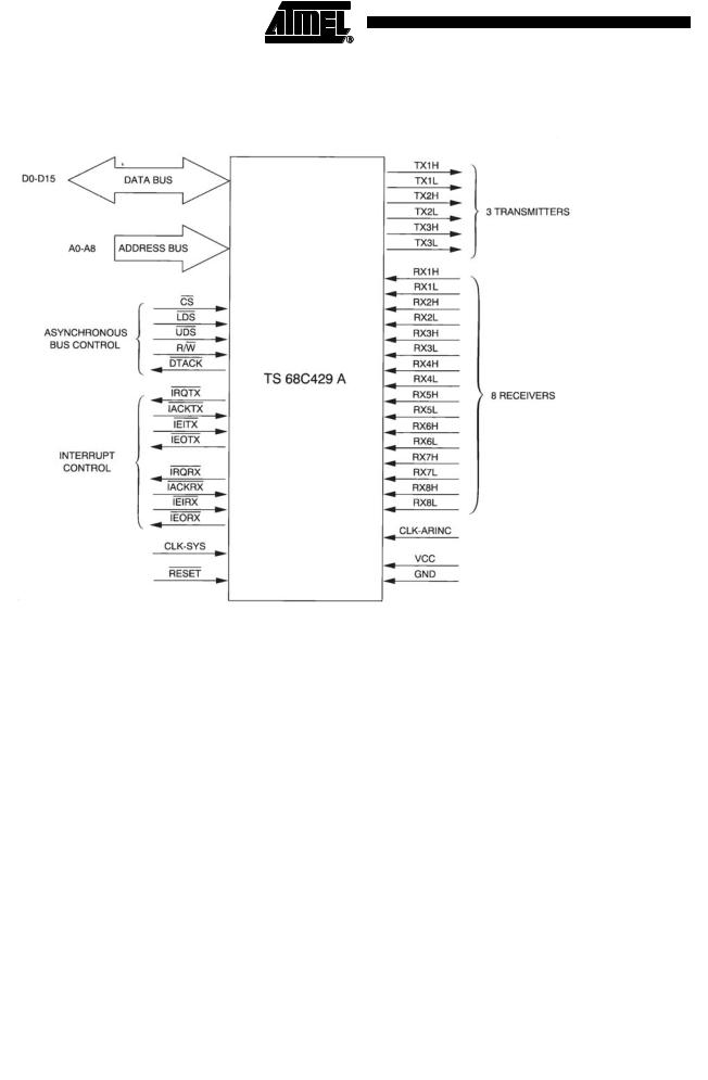
Figure 2 illustrates the functional signal groups.
Figure 2. Functional Signal Groups Diagram
Scope
Applicable
Documents
MIL-STD-883
This drawing describes the specified requirements for the ARINC multi channel receiver/transmitter, in compliance either with MIL-STD-863 class B or SMD drawing.
1.MIL-STD-883: test methods and procedures for electronics
2.MIL-STD-38535: general specifications for microcircuits.
3.MIL-STD-1835 microcircuit case outlines.
4.DESC/SMD.
Requirements
General |
The microcircuits are in accordance with the applicable document and as specified |
|
herein. |
6 TS68C429A 
2120A–HIREL–08/02

|
|
|
|
TS68C429A |
|
|
|
|
|
|
Design and Construction |
|
|
|
|
|
|
|
|
|
|
|
|
|
|
Terminal Connections |
Depending on the package, the terminal connections is detailed in “Terminal Connec- |
||
|
|
tions” on page 41. |
||
|
Package |
The circuits are packaged in a hermetically sealed ceramic package which is conform to |
||
|
|
case outlines of MIL-STD 1835 (when defined): |
||
|
|
• |
PGA 84, |
|
|
|
• |
CQFP 132. |
|
Special Recommended Conditions for CMOS Devices
The precise case outlines are described at the end of this specification (“Package Mechanical Data” on page 40) and into MIL-STD-1835.
• CMOS Latch-up
The CMOS cell is basically composed of two complementary transistors (a P-channel and an N-channel), and, in the steady state, only one transistor is turned-on. The active P-channel transistor sources current when the output is a logic high and presents a high impedance when the output is a logic low. Thus the overall result is extremely low power consumption because there is no power loss through the active P-channel transistor. Also since only once transistor is determined by leakage currents.
Because the basic CMOS cell is composed of two complementary transistors, a parasitic semiconductor controlled rectifier (SCR) formed and may be triggered when an input exceeds the supply voltage. The SCR that is formed by this high input causes the device to become “latched” in a mode that may result in excessive current drain and eventual destruction of the device. Although the device is implemented with input protection diodes, care should be exercised to ensure that the maximum input voltages specification is not exceeded from voltage transients; others may require no additional circuitry.
• CMOS/TTL Levels
The TS68C429A doesn’t satisfy totally the input/output drive requirements of TTL logic devices, see Table 4.
Electrical Characteristics
Table 1. Absolute Maximum Ratings
Symbol |
Parameter |
Test Conditions |
Min |
Max |
Unit |
|
VCC |
Supply Voltage |
|
-0.3 |
+7.0 |
V |
|
VI |
Input Voltage |
|
-0.3 |
+7.0 |
V |
|
Pdmax |
Max Power Dissipation |
|
|
400 |
mW |
|
Tcase |
Operating Temperature |
M suffix |
-55 |
+125 |
°C |
|
|
|
|
|
|||
V suffix |
-40 |
+85 |
°C |
|||
|
|
|||||
|
|
|
|
|
|
|
Tstg |
Storage Temperature |
|
-55 |
+150 |
°C |
|
Tj |
Junction Temperature |
|
|
+160 |
°C |
|
Tleads |
Lead Temperature |
Max 5 sec. soldering |
|
+270 |
°C |
7
2120A–HIREL–08/02

Unless otherwise stated, all voltages are referenced to the reference terminal.
Table 2. Recommended Condition of Use
Symbol |
Parameter |
Test conditions |
Min |
Max |
Units |
|
VCC |
Supply Voltage |
|
4.5 |
5.5 |
V |
|
VIL |
Low Level Input Voltage |
|
-0.5 |
0.8 |
V |
|
VIH |
High Level Input Voltage |
|
2.25 |
5.8 |
V |
|
Tcase |
Operating Temperature |
M suffix |
-55 |
+125 |
°C |
|
|
|
|
|
|||
V suffix |
-40 |
+85 |
°C |
|||
|
|
|||||
|
|
|
|
|
|
|
CL |
Output Loading Capacitance |
|
|
130 |
pF |
|
tr(c) |
Clock Rise Time (See Figure 3) |
|
|
5 |
ns |
|
tf(c) |
Clock Fall Time (See Figure 3) |
|
|
5 |
ns |
|
fc |
Clock System Frequency |
|
0.5 |
20 |
MHz |
|
(See Figure 3) |
|
|||||
|
|
|
|
|
||
|
|
|
|
|
|
This device contains protective circuitry against damage due to high static voltages or electrical fields: however, it is advised that normal precautions be taken to avoid application of any voltages higher than maximum-rated voltages to this high-impedance circuit. Reliability of operation is enhanced if unused inputs are tied to an appropriate logic voltage level (e.g., either GND or VCC).
Figure 3. Clock Input Timing Diagram
|
|
|
|
|
|
|
|
|
|
|
|
|
|
|
|
|
|
|
|
|
|
|
|
|
tcyc |
|
|
|
||||||||
|
|
|
|
|
|
|
|
|
|
|
|
|
|
|
|
|
|
|
|
|
|
|
|
|
|
|
|
|||||||||
2.25V |
|
|
|
|
|
|
|
|
|
|
|
|
|
|
|
|
|
tCL |
|
|
|
|
|
|
|
tCH |
|
|
|
|||||||
|
|
|
|
|
|
|
|
|
|
|
|
|
|
|
|
|
|
|
|
|
|
|
|
|
|
|
||||||||||
|
|
|
|
|
|
|
|
|
|
|
|
|
|
|
|
|
|
|
|
|
|
|
|
|
|
|
|
|
|
|
||||||
|
|
|
|
|
|
|
|
|
|
|
|
|
|
|
|
|
|
|
|
|
|
|
|
|
|
|
|
|
|
|||||||
|
|
|
|
|
|
|
|
|
|
|
|
|
|
|
|
|
|
|
|
|
|
|
|
|
|
|
|
|
|
|||||||
0.8V |
|
|
|
|
|
|
|
|
|
|
|
|
|
|
|
|
|
|
|
|
|
|
|
|
|
|
|
|
|
|
|
|
|
|
||
|
|
|
|
|
|
|
|
|
|
|
|
|
|
|
|
|
|
|
|
|
|
|
|
|
|
|
|
|
|
|
|
|
|
|
||
|
|
|
|
|
|
|
|
|
|
|
|
|
|
|
|
|
|
|
|
|
|
|
|
|
|
|
|
|
|
|
||||||
|
|
|
|
|
|
|
|
|
|
|
|
|
|
|
|
|
|
|
|
|
|
|
|
|
|
|
|
|
|
|
|
|
|
|
|
|
tCR |
|
|
|
|
|
|
|
|
|
|
|
|
|
|
|
|
|
|
|
|
|
|
tCF |
|
|
|
|
|
|
|
|
|
|
|
|
|
|
|
|
|
|
|
|
|
|
|
|
|
|
|
|
|
|
|
|
|
|
|
|
|
|
|
|
|
|
|
|
|
|||||
Note: Timing measurements are referenced to and from a low of 0.8-volt and a high voltage of 2.25 volts, unless otherwise noted. The voltage swing through this range should start outside and pass through the range such that the rise or fall will be linear between 0.8-volt and 2.25 volts.
Table 3. Thermal Characteristics
Package |
Symbol |
Parameter |
Value |
Unit |
|
|
|
|
|
|
|
PGA 68 |
θJ-A |
Thermal Resistance Junction-to-ambient |
28 |
°C/W |
|
θJ-C |
Thermal Resistance Junction-to-case |
2 |
°C/W |
||
|
|||||
CQFP 132 |
θJ-A |
Thermal Resistance Junction-to-ambient |
27 |
°C/W |
|
θJ-C |
Thermal Resistance Junction-to-case |
3 |
°C/W |
||
|
8 TS68C429A 
2120A–HIREL–08/02

|
|
|
|
TS68C429A |
|
|
|
|
|
|
Power Considerations |
|
|
|
|
The average chip-junction temperature, TJ, in °C can be obtained from: |
|||
|
||||
|
|
TJ = TA + (PD θJA) |
(1) |
|
TA = Ambient Temperature, °C
θJA = Package Thermal Resistance, Junction-to-Ambient, °C/W
PD = PINT + PI/O
PINT = ICC x VCC, Watts—Chip Internal Power
PI/O = Power Dissipation on Input and Output Pins—User Determined For most applications PI/O < PINT and can be neglected.
An approximate relationship between PD and TJ (if PI/O is neglected) is:
PD = K: (TJ + 273) |
(2) |
Solving equations (1) and (2) for K gives:
K = P |
D |
(T |
A |
+ 273) + θ |
JA |
P |
2 |
(3) |
|
|
|
|
D |
|
Mechanical and
Environment
Marking
where K is a constant pertaining to the particular part K can be determined from equation (3) by measuring PD (at equilibrium) for a known TA. Using this value of K, the values of PD and TJ can be obtained by solving equations (1) and (2) iteratively for any value of TA.
The total thermal resistance of a package (θJA) can be separated into two components, θJC and θCA, representing the barrier to heat flow from the semiconductor junction to the package (case), surface (θJC) and from the case to the outside ambient (θCA). These terms are related by the equation:
θJA = θJC + θCA |
(4) |
θJC is device related and cannot be influenced by the user. However, θCA is user dependent and can be minimized by such thermal management techniques as heat sinks, ambient air cooling and thermal convection. Thus, good thermal management on the part of the user can significantly reduce θCA so that θJA approximately equals θJC. Substitution of θJC for θJA in equation (1) will result in a lower semiconductor junction temperature.
The microcircuits shall meet all mechanical environmental requirements of either MIL- STD-883 for class B devices or DESC devices.
The document where are defined the marking are identified in the related reference documents. Each microcircuit are legibly and permanently marked with the following information as minimum:
•Atmel logo
•Manufacturer’s part number
•Class B identification
•Date-code of inspection lot
•ESD identifier if available
•Country of manufacturing
9
2120A–HIREL–08/02

Quality Conformance
Inspection
DESC/MIL-STD-883
Is in accordance with MIL-M-38510 and method 5005 of MIL-STD-883. Group A and B inspections are performed on each production lot. Group C and D inspections are performed on a periodic basis.
Electrical
Characteristics
General Requirements
All static and dynamic electrical characteristics specified for inspection purposes and the relevant measurement conditions are given below:
•Table 4, Table 5: Static electrical characteristics for the electrical variants.
•Table 6, Table 7, Table 8: Dynamic electrical characteristics.
For static characteristics (Table 4, Table 5), test methods refer to IEC 748-2 method number, where existing.
For dynamic characteristics (Table 6, Table 7, Table 8), test methods refer to clause 5.5 of this specification.
Table 4. DC Electrical Characteristics
With -55°C ≤ Tcase ≤ +125°C or -40° ≤ Tcase ≤ +85°C; VCC = 5V ± 10%.
Symbol |
Parameter |
|
Min |
Max |
Unit |
||||||
VIH |
|
Input High Voltage |
|
2.25 |
VCC + 0.3 |
V |
|||||
VIL |
|
Input Low Voltage |
|
-0.5 |
0.8 |
V |
|||||
VOH |
|
Output High Voltage (except |
|
|
|
|
|
open drain outputs) |
2.7 |
|
V |
|
IRQRX, |
IRQTX: |
|
||||||||
VOL |
|
Output Low Voltage |
|
|
0.5 |
V |
|||||
|
|
Output Source Current (except |
|
|
|
|
|
|
|
|
|
IOH |
|
IRQRX, |
(Vout = 2.7V) |
|
-8 |
mA |
|||||
|
IRQTX: open drain outputs) |
|
|||||||||
|
|
|
|
|
|
||||||
|
|
|
|
|
|
|
|||||
IOL |
|
Output Sink Current |
(Vout = 0.5V) |
|
8 |
mA |
|||||
ILI |
|
Input Leakage Current |
(Vin = 0 to VCC) |
|
±20 |
µA |
|||||
IDD |
|
Dynamic Current(1) |
(Tcase = Tmin VDD |
|
65 |
mA |
|||||
|
|
|
|
|
|
|
|
= Vmax) |
|
|
|
Note: 1. |
IDD is measured with all I/O pins at 0V, all input pins at 0V except signals CS, IACKxx, LDS, UDS at 5V and CLK-SYS and |
||||||||||
|
CLK-ARINC which run at tcyc mini. |
|
|
|
|
||||||
Table 5. Capacitance (TA = 25°C)
Symbol |
Parameter |
Max |
Unit |
Cin |
Input Capacitance |
10 |
pF |
Cout |
HI-Z Output Capacitance |
20 |
pF |
10 TS68C429A 
2120A–HIREL–08/02
|
|
|
|
|
|
|
|
|
|
|
|
TS68C429A |
|
|
|
|
|
|
|
|
|
|
|
|
|
||
|
Clock Timing |
|
|
|
|
|
|
|
|
|
|||
|
|
|
|
|
|
|
|
|
|
|
|
||
|
|
|
|
|
|
|
|
|
|
|
|
||
|
Table 6. Clock System (CLK SYS) |
|
|
|
|
|
|||||||
|
|
Symbol |
Parameter |
|
Min |
Max |
|
Unit |
|||||
|
|
|
|
|
|
|
|
|
|||||
|
|
tcyc S |
Clock Period |
|
50 |
2000 |
|
ns |
|||||
|
|
tCLS, tCHS |
Clock Pulse Width |
|
20 |
|
|
ns |
|||||
|
|
tcrS, tcfS |
Rise and Fall Times |
|
|
5 |
|
ns |
|||||
|
Table 7. Clock ARINC (CLK ARINC) |
|
|
|
|
|
|||||||
|
|
Symbol |
Parameter |
|
Min |
Max |
|
Unit |
|||||
|
|
|
|
|
|
|
|
|
|||||
|
|
tcyc A |
Cycle Time(1) |
|
200 |
8000 |
|
ns |
|||||
|
|
tCLA, tCHA |
Clock Pulse Width |
|
240 |
|
|
ns |
|||||
|
|
tcrA, tcfA |
Rise and Fall Times |
|
|
5 |
|
ns |
|||||
|
Note: 1. |
tcyc A ≥ 4 x tcyc S. |
|
|
|
|
|
|
|
|
|
|
|
|
AC Electrical |
|
With VCC = 5 VDC ± 10% VSS = 0 VDC. |
|
|
|
|||||||
|
Characteristics |
|
|
|
|
|
|
must be understood as generic signals (xx = RX and TX). |
|||||
|
|
IEIxx, |
IEOxx, |
IACKxx, |
|||||||||
|
Figure 4. |
Read Cycle |
|
|
|
|
|
|
|
|
|
|
|
Notes: 1. LDS/UDS can be asserted on the next or previous CLK-SYS period after CS goes low but (4) must be met for the next period.
2. The cycle ends when the first of CS, LDS/UDS goes high.
11
2120A–HIREL–08/02

Figure 5. Write Cycle
3. LDS/UDS can be asserted on the same or previous CLK-SYS period as CS but (3) and (4) must be met.
Figure 6. Interrupt Cycle (IEIxx = 0)
Notes: 1. If UDS = 1, D15-D8 stay hi-z else D15-D8 drive the bus with a stable unknown value.
2.If IEOxx goes low, neither vector nor DTACK are generated, else IEOxx stays inactive and a vector is generated (D7-D0 and DTACK).
12 TS68C429A 
2120A–HIREL–08/02
TS68C429A
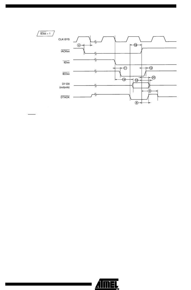
Figure 7. Interrupt Cycle (IEIxx = 1)
Notes: 1. If UDS = 1, D15-D8 stay hi-z else D15-D8 drive the bus with a stable unknown value.
2.If IEOxx goes low, neither vector nor DTACK are generated, else IEOxx stays inactive and a vector is generated (D7-D0 and DTACK).
Table 8. Timing Characteristic
Number |
Symbol |
Parameter |
Min |
Max |
T/G(1) |
Unit |
||||||||||||||||||||||||||||||||||||||||||||
1 |
tAVCSL |
|
Address valid to |
|
|
|
|
|
|
low |
0 |
- |
T |
ns |
||||||||||||||||||||||||||||||||||||
CS |
||||||||||||||||||||||||||||||||||||||||||||||||||
2 |
tRWVCSL |
|
R/W valid to |
|
|
|
|
|
|
|
|
low |
0 |
- |
T |
ns |
||||||||||||||||||||||||||||||||||
CS |
||||||||||||||||||||||||||||||||||||||||||||||||||
3 |
tDIVDSL |
|
Data in valid to |
|
|
|
|
|
|
|
|
|
|
|
|
|
|
|
|
|
|
|
|
|
|
|
|
0 |
- |
T |
ns |
|||||||||||||||||||
LDS/UDS low |
||||||||||||||||||||||||||||||||||||||||||||||||||
4 |
tSVCL |
|
CS, |
|
|
|
|
|
|
|
|
|
|
|
|
|
|
|
|
|
|
|
|
|
|
|
|
|
|
|
|
|
|
|
|
|
|
|
|
|
|
|
|
|
5 |
- |
T |
ns |
||
LDS/UDS, IACKxx valid to CLK-SYS low |
||||||||||||||||||||||||||||||||||||||||||||||||||
5 |
tCLDKL |
|
CLK-SYS low to |
|
|
|
|
|
|
|
|
|
low |
- |
45 |
T |
ns |
|||||||||||||||||||||||||||||||||
DTACK |
||||||||||||||||||||||||||||||||||||||||||||||||||
6 |
tCLDOV |
|
CLK-SYS low to data out valid |
- |
50 |
T |
ns |
|||||||||||||||||||||||||||||||||||||||||||
7 |
tDKLDOV |
|
|
|
|
|
|
|
|
|
low to data out valid |
- |
10 |
G |
ns |
|||||||||||||||||||||||||||||||||||
|
DTACK |
|||||||||||||||||||||||||||||||||||||||||||||||||
8 |
tSHDKH |
|
|
|
or |
|
|
|
|
|
|
|
|
|
|
|
|
|
|
|
|
|
|
|
|
|
|
|
|
|
|
|
|
|
|
|
|
|
|
|
|
|
|
|
- |
35 |
G |
ns |
||
|
CS |
LDS/UDS or IACKxx high to DTACK high |
||||||||||||||||||||||||||||||||||||||||||||||||
9 |
tSHDXZ |
|
|
|
or |
|
|
|
|
|
|
|
|
|
|
|
|
|
|
|
|
|
|
|
|
|
|
|
|
|
|
|
|
|
|
|
|
|
|
|
|
|
|
|
- |
50 |
G |
ns |
||
|
CS |
LDS/UDS or IACKxx high to DTACK hi-z |
||||||||||||||||||||||||||||||||||||||||||||||||
10 |
tSHDOZ |
|
|
|
or |
|
|
|
|
|
|
|
|
|
|
|
|
|
|
|
|
|
|
|
|
|
|
|
|
|
|
|
|
|
|
|
|
|
|
|
|
|
|
|
- |
25 |
G |
ns |
||
|
CS |
LDS/UDS or IACKxx high to data out hi-z |
||||||||||||||||||||||||||||||||||||||||||||||||
11 |
tILIOL |
|
|
|
|
|
or |
|
|
|
|
|
|
|
|
|
|
|
|
|
low to |
|
|
|
|
|
low |
- |
35 |
T |
ns |
|||||||||||||||||||
|
IEIxx |
IACKxx |
IEOxx |
|||||||||||||||||||||||||||||||||||||||||||||||
12 |
tIKHIOH |
|
|
|
|
|
|
|
high to IEOxx high |
- |
40 |
T |
ns |
|||||||||||||||||||||||||||||||||||||
|
IACKxx |
|||||||||||||||||||||||||||||||||||||||||||||||||
13 |
tIILDKL |
|
|
|
|
|
low to |
|
|
|
|
|
|
|
|
|
|
|
|
|
|
|
low |
- |
40 |
T |
ns |
|||||||||||||||||||||||
|
IEIxx |
DTACK |
||||||||||||||||||||||||||||||||||||||||||||||||
14 |
tIILDOV |
|
|
|
|
|
low to data out valid |
- |
45 |
T |
ns |
|||||||||||||||||||||||||||||||||||||||
|
IEIxx |
|||||||||||||||||||||||||||||||||||||||||||||||||
15 |
tSH |
|
|
|
|
|
|
|
|
|
|
|
|
|
|
|
|
|
|
|
|
|
|
|
|
|
|
|
|
|
|
|
|
|
|
|
|
|
|
|
|
|
|
15 |
- |
T |
ns |
|||
|
CS, |
IACKxx, |
LDS/UDS inactive time |
|||||||||||||||||||||||||||||||||||||||||||||||
16 |
tDKLSH |
|
|
|
|
|
|
|
|
low to |
|
|
|
|
|
|
|
|
|
or |
|
|
|
|
|
|
|
|
|
|
|
|
0 |
- |
G |
ns |
||||||||||||||
|
DTACK |
CS |
LDS/UDS or IACKxx high |
|||||||||||||||||||||||||||||||||||||||||||||||
17 |
tSHAH |
|
|
|
or |
|
|
|
|
|
|
|
|
|
|
|
|
|
|
|
|
|
|
|
|
|
|
|
|
|
|
|
|
|
|
|
|
|
|
|
|
|
|
|
0 |
- |
G |
ns |
||
|
CS |
LDS/UDS high to address hold time |
||||||||||||||||||||||||||||||||||||||||||||||||
13
2120A–HIREL–08/02
Loading...