


 Loading...
ATMEL TS68882VR33, TS68882VR25, TS68882VR20, TS68882VR16, TS68882VF33 Datasheet
...Features
•Eight General-purpose Floating-point Data Registers, Each Supporting a Full 80-bit Extended Precision Real Data Format (a 64-bit Mantissa Plus a Sign Bit, and a 15-bit Signed Exponent)
•A 67-bit Arithmetic Unit to Allow Very Fast Calculations with Intermediate are Precision Greater than the Extended Precision Format
•A 67-bit Barrel Shifter for High-speed Shifting Operations (for Normalizing etc.)
•Special-purpose Hardware for High-speed Conversion Between Single, Double, and Extended Formats and the Internal Extended Format
•An Independent State Machine to Control Main Processor Communication for Pipelined Instruction Processing
•Forty-six Instructions, Including 35 Arithmetic Operations
•Full Conformation to the IEEE 754 Standard, Including All Requirements and Suggestions
•Support of Functions Not Defined by the IEEE Standard, Including a Full Set of Trigonometric and Transcendental Functions
•Seven Data Type Types: Byte, Word and Long Integers; Single, Double, and Extended Precision Real Numbers; and Packed Binary Coded Decimal String Real Numbers
•Twenty-two Constants Available In The On-chip ROM, Including π, e, and Powers of 10
•Virtual Memory/Machine Operations
•Efficient Mechanisms for Procedure Calls, Context Switches, and Interrupt Handling
•Fully Concurrent Instruction Execution with the Main Processor
•Fully Concurrent Instruction Execution of Multiple Floating-point Instructions
•Use with any Host Processor, on an 8-, 16or 32-bit Data Bus
•Available in 16.67, 20, 25 and 33 MHz for Tc from -55°C to +125°C
•VCC = 5V ± 10%
Description
The TS68882 enhanced floating-point co-processor is a full implementation of the IEEE Standard for Binary Floating-Point Arithmetic (754) for use with the THOMSON TS68000 Family of microprocessors. It is a pin and software compatible upgrade of the TS68881 with optimized MPU interface that provides over 1.5 times the performance of the TS68881. It is implemented using VLSI technology to give systems designers the highest possible functionality in a physically small device.
Intended primarily for use as a co-processor to the TS68020/68030 32-bit microprocessor units (MPUs), the TS68882 provides a logical extension to the main MPU integer data processing capabilities. It does this by providing a very high performance floating-point arithmetic unit and a set of floating-point data registers that are utilized in a manner that is analogous to the use of the integer data registers. The TS68882 instruction set is a natural extension of all earlier members of the TS68000 Family, and supports all of the addressing modes of the host MPU. Due to the flexible bus interface of the TS68000 Family, the TS68882 can be used with any of the MPU devices of the TS68000 Family, and it may also be used as a peripheral to non-TS68000 processors.
Screening/Quality
This product could be manufactured |
R suffix |
F suffix |
|
PGA 68 |
CQFP 68 |
||
in full compliance with either: |
Ceramic Pin Grid Array |
Ceramic Quad Flat Pack |
|
|
|
||
• |
MIL-STD-883 Class B |
|
|
• |
DESC 5962-89436 |
|
|
• or According to ATMELGrenoble Standards
CMOS |
Enhanced |
Floating-point |
Co-processor |
TS68882 |
Rev. 2119A–HIREL–04/02 |
1 |

Introduction
The TS68882 is a high-performance floating-point device designed to interface with the TS68020 or TS68030 as a co-processor. This device fully supports the TS68000 virtual machine architecture, and is implemented in HCMOS, Atmel’s low power, small geometry process. This process allows CMOS and HMOS (high-density NMOS) gates to be combined on the same device. CMOS structures are used where speed and low power is required, and HMOS structures are used where minimum silicon area is desired. The HCMOS technology enables the TS68882 to be very fast while consuming less power than comparable HMOS, and still have a reasonably small die size.
With some performance degradation, the TS68882 can also be used as a peripheral processor in systems where the TS68020 or TS68030 is not the main processor (i.e., TS68000, TS68010). The configuration of the TS68882 as a peripheral processor or coprocessor may be completely transparent to user software (i.e., the same object code may be executed in either configuration).
The architecture of the TS68882 appears to the user as a logical extension of the TS68000 Family architecture. Coupling of the co-processor interface allows the TS68020/TS68030 programmer to view the TS68882 registers as though the registers are resident in the TS68020/TS68030. Thus, a TS68020 or TS68030/TS68882 device pair appears to be one processor that supports seven floating-point and integer data types, and has eight integer data registers, eight address registers, and eight floatingpoint data registers.
As shown in Figure 1, the TS68882 is internally divided into four processing elements; the Bus Interface Unit (BIU), the Conversion Control Unit (CCU), the Execution Control Unit (ECU), and the Microcode Control Unit (MCU). The BIU communicates with the main processor, the CCU controls the main processor communications dialog and performs some data conversions, and the ECU and MCU execute most floating-point calculations.
The BIU contains the co-processor interface registers, and the 32-bit control, and instruction address registers. In addition to these registers, the register select and DSACK timing control logic is contained in the BIU. Finally, the status flags used to monitor the status of communications with the main processor are contained in the BIU.
The CCU contains special-purpose hardware that performs conversions between the single, double, and extended precision memory data formula and the internal data format used by the ECU. It also contains a state machine that controls communications with the main processor during co-processor interface dialogs.
The eight 80-bit floating-point data registers (FP0-FP7) are located in the ECU. In addition to these registers, the ECU contains a high-speed 67-bit arithmetic unit used for both mantissa and exponent calculations, a barrel shifter that can shift from 1-bit to 67bits in one machine cycle, and ROM constants (for use by the internal algorithms or user programs).
The MCU contains the clock generator, a two-level microcoded sequencer that controls the ECU, the microcode ROM, and self-test circuitry. The built-in self-test capabilities of the TS68882 enhance reliability and ease manufacturing requirements; however, these diagnostic functions are not available to the user.
2 TS68882
2119A–HIREL–04/02

TS68882
Figure 1. TS68882 Simplified Block
3
2119A–HIREL–04/02
Pin Assignments
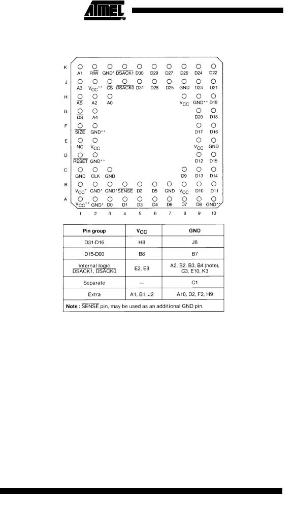
Figure 2. PGA Terminal Designation
* Reserved for future ATMEL-Grenoble use
4 TS68882
2119A–HIREL–04/02
TS68882
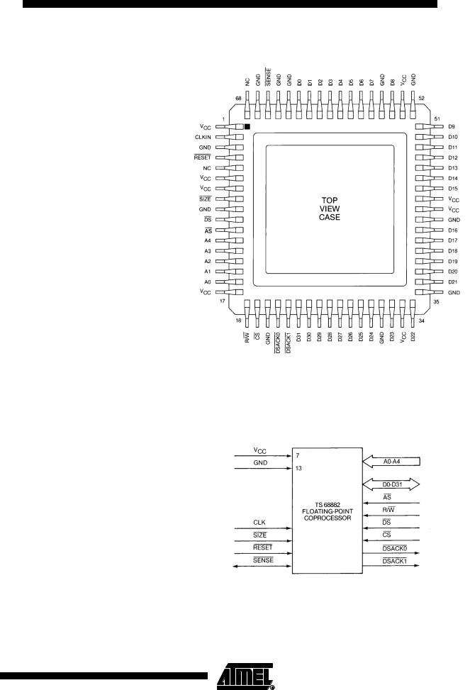
Figure 2b. CQFP Terminal Designation
Functional Signal
Descriptions
This section contains a brief description of the input and output signals for the TS68882 floating-point co-processor. The signals are functionally organized into groups as shown in Figure 3.
Figure 3. TS68882 Input/output Signals
Note: The terms assertion and negation are used extensively. This is done to avoid confusion when describing “active-low” and “active-high” signals. The term assert or assertion is used to indicate that a signal is active or true, independent of whether that level is represented by a high or low voltage. The term negate or negation is used to indicate that a signal is inactive or false.
5
2119A–HIREL–04/02

Signal Summary |
|
|
|
|
|
|
|
|
|
|
|
|
|
|
|
|
|
|
|
|
|
|
|
|
|
|
|
|
|
|
|
|
|
|
|
|
|
|
|
|
|
|
|
|
|
Table 1 provides a summary of all the TS68882 signals described in this section. |
||||||||||||||||||||||
Table 1. Signal Summary |
|
|
|
|
|
|
|
|
|
|
|
|
|
|
|
|
|
|
|
|
|
|
|
|
|
|
|
|
|
|
|||||||||||||||
Signal Name |
|
|
Mnemonic |
|
Input/Output |
Active State |
Three State |
|||||||||||||||
|
|
|
|
|
|
|
|
|
||||||||||||||
Address Bus |
|
|
|
A0 - A4 |
|
Input |
High |
|
||||||||||||||
|
|
|
|
|
|
|
|
|||||||||||||||
Data Bus |
|
|
D0 - D31 |
|
Input/Output |
High |
Yes |
|||||||||||||||
|
|
|
|
|
|
|
|
|
|
|
|
|
|
|
|
|
|
|
|
|
||
Size |
|
|
|
|
|
|
|
|
|
|
|
|
|
|
|
|
|
Input |
Low |
|
||
|
|
|
|
SIZE |
|
|||||||||||||||||
|
|
|
|
|
|
|
|
|
|
|
|
|
|
|
|
|
|
|
|
|||
Address Strobe |
|
|
|
|
|
|
|
|
|
|
|
|
|
|
|
|
Input |
Low |
|
|||
|
|
|
|
|
AS |
|
||||||||||||||||
|
|
|
|
|
|
|
|
|
|
|
|
|
|
|
|
|
|
|
||||
Chip Select |
|
|
|
|
|
|
|
|
|
|
|
|
|
|
|
|
Input |
Low |
|
|||
|
|
|
|
|
CS |
|
||||||||||||||||
|
|
|
|
|
|
|
|
|
|
|
|
|
|
|
|
|
||||||
Read/Write |
|
|
|
|
|
|
|
|
|
|
|
|
|
|
|
|
Input |
High/Low |
|
|||
|
|
|
|
R/W |
|
|||||||||||||||||
|
|
|
|
|
|
|
|
|
|
|
|
|
|
|
|
|
||||||
Data Strobe |
|
|
|
|
|
|
|
|
|
|
|
|
|
|
|
Input |
Low |
|
||||
|
|
|
|
|
DS |
|
||||||||||||||||
|
|
|
|
|
|
|
|
|
|
|
|
|
|
|||||||||
Data Transfer and Size Acknowledge |
|
|
|
|
|
|
|
|
|
|
|
|
|
|
|
|
|
|
Output |
Low |
Yes |
|
DSACK0, |
DSACK1 |
|||||||||||||||||||||
|
|
|
|
|
|
|
|
|
|
|
||||||||||||
Reset |
|
|
|
|
|
|
|
|
|
|
|
|
|
|
|
|
Input |
Low |
|
|||
|
|
|
RESET |
|
||||||||||||||||||
|
|
|
|
|
|
|
|
|
|
|||||||||||||
Clock |
|
|
|
|
CLK |
|
Input |
|
|
|||||||||||||
|
|
|
|
|
|
|
|
|
|
|||||||||||||
Sense Device |
|
|
|
|
|
|
|
|
|
|
|
|
|
|
|
|
Input/Output |
Low |
No |
|||
|
|
SENSE |
||||||||||||||||||||
|
|
|
|
|
|
|
|
|
|
|||||||||||||
Power Input |
|
|
|
|
VCC |
|
Input |
|
|
|||||||||||||
Ground |
|
|
|
|
GND |
|
Input |
|
|
|||||||||||||
|
|
|
|
|
|
|
|
|
|
|
|
|
|
|
|
|
|
|
|
|
|
|
Detailed
Specifications
Scope
Applicable Documents
This drawing describes the specific requirements for the microprocessor 68882, 16.67, 20 MHz and 25 MHz, in compliance with MIL-STD-883 class B.
MIL-STD-883 |
1. |
MIL-STD-883: Test Methods And Procedures For Electronics |
|
2. |
MIL-PRF-38535 Appendix A: General Specifications For Microcircuits |
|
3. |
Desc Drawing 5962 - 89436xxx |
Requirements
General |
The microcircuits are in accordance with the applicable document and as specified |
|
herein. |
Design and Construction
Terminal Connections |
Depending on the package, the terminal connections shall be as shown in Figure 2 and |
|
Figure 2b. |
Lead Material and Finish |
Lead material and finish shall be any option of MIL-STD-1835. |
6 TS68882
2119A–HIREL–04/02

|
|
|
TS68882 |
|
|
|
|
Package |
|
||
The macrocircuits are packaged in hermetically sealed ceramic packages which are |
|||
|
|
conform to case outlines of MIL-STD-1835 (when defined): |
|
|
|
• 68-PIN SQ.PGA UP PAE Outline |
|
|
|
• 68-PIN Ceramic Quad Flat Pack CQFP |
|
|
|
The precise case outlines are described on Figure 23 and Figure 24. |
|
Electrical
Characteristics
Table 2. Absolute Maximum Ratings
Symbol |
Parameter |
Test Conditions |
Min |
Max |
Unit |
|
|
|
|
|
|
|
|
VCC |
Supply Voltage |
|
-0.3 |
+7.0 |
V |
|
VI |
Input Voltage |
|
-0.3 |
+7.0 |
V |
|
|
|
|
|
|
|
|
PDMAX |
|
|
TCASE = -55°C to |
|
0.75 |
W |
Max Power Dissipation |
+125°C |
|
||||
|
|
|
|
|||
|
|
|
|
|
|
|
TCASE |
Operating Temperature |
|
M Suffix |
-55 |
+125 |
°C |
|
|
|
|
|
||
|
V Suffix |
-40 |
+85 |
°C |
||
|
|
|
||||
|
|
|
|
|
|
|
TSTG |
Storage Temperature |
|
-55 |
+150 |
°C |
|
TLEADS |
Lead Temperature |
Max 5 sec. Soldering |
|
+270 |
°C |
|
Recommended Condition of |
Unless otherwise stated, all voltages are referenced to the reference terminal (see |
||||||||||||||||||||||||||||||||
Use |
|
|
|
|
Table 1). |
|
|
|
|||||||||||||||||||||||||
Table 3. DC Electrical Characteristics |
|
|
|
||||||||||||||||||||||||||||||
VCC = 5.0 VDC ± 10%; GND = 0 VDC; Tc = -55°C to +125°C |
|
|
|
||||||||||||||||||||||||||||||
Symbol |
Parameter |
|
|
|
|
|
|
|
|
|
|
|
|
|
|
|
|
|
|
|
|
|
|
|
|
|
|
|
|
Min |
Max |
Unit |
|
|
|
|
|
|
|
|
|
|
|
|
|
|
|
|
|
|
|
|
|
|
|
|
|
|
|
|
|
|
|
|
|
|
|
VCC |
Supply Voltage |
|
|
|
|
|
|
|
|
|
|
|
|
|
|
|
|
|
|
|
|
|
|
|
|
|
|
|
|
4.5 |
5.5 |
V |
|
TCASE |
Operating Temperature |
|
|
|
|
|
|
|
|
|
|
|
|
|
|
|
|
|
|
|
|
|
|
|
|
|
|
-55 |
+125 |
°C |
|||
VIH |
Input High Voltage |
|
|
|
|
|
|
|
|
|
|
|
|
|
|
|
|
|
|
|
|
|
|
|
|
|
|
2.0 |
VCC |
V |
|||
VIL |
Input Low Voltage |
|
|
|
|
|
|
|
|
|
|
|
|
|
|
|
|
|
|
|
|
|
|
|
|
|
|
GND - 0.3 |
0.8 |
V |
|||
IIN |
Input Leakage Current at 5.5V |
|
|
|
|
|
|
|
|
|
|
|
|
|
|
|
|
|
|
|
|
|
|
|
|
|
|
|
|
||||
CLK, |
RESET, |
R/W, |
|
A0-A4, CS, DS, AS, SIZE |
|
10 |
µA |
||||||||||||||||||||||||||
ITSI |
HI-Z (Off state) Input Current at 2.4V/0.4V |
|
|
|
|
|
|
|
|
|
|
|
|
|
D0-D31 |
|
20 |
µA |
|||||||||||||||
DSACK0, |
DSACK1, |
|
|||||||||||||||||||||||||||||||
V |
|
Output High Voltage (IOH = -400 µA)(1) |
|
|
|
|
|
|
|
|
|
|
|
D0-D31 |
2.4 |
|
V |
||||||||||||||||
|
DSACK0, |
DSACK1, |
|
||||||||||||||||||||||||||||||
OH |
|
|
|
|
|
|
|
|
|
|
|
|
|
|
|
|
|
|
|
|
|
|
|
|
|
|
|
|
|
|
|
|
|
V |
|
Output Low Voltage (IOL = 5.3 mA)(1) |
|
|
|
|
|
|
|
|
|
|
|
D0-D31 |
|
0.5 |
V |
||||||||||||||||
|
DSACK0, |
DSACK1, |
|
||||||||||||||||||||||||||||||
OL |
|
|
|
|
|
|
|
|
|
|
|
|
|
|
|
|
|
|
|
|
|
|
|
|
|
|
|
|
|
|
|
|
|
IOL |
Output Low Current (VOL = GND) SENSE |
|
500 |
µA |
|||||||||||||||||||||||||||||
PD |
Power Dissipation |
|
|
|
|
|
|
|
|
|
|
|
|
|
|
|
|
|
|
|
|
|
|
|
|
|
|
|
0.75 |
W |
|||
C |
IN |
Capacitance (V |
IN |
= 0, T = 25°C, f = 1 MHz)(2) |
|
20 |
pF |
||||||||||||||||||||||||||
|
|
|
A |
|
|
|
|||||||||||||||||||||||||||
CL |
Output Load Capacitance |
|
130 |
pF |
|||||||||||||||||||||||||||||
Notes: 1. Test load, see Figure 5. |
|
|
|
|
|
|
|
|
|
|
|
|
|
|
|
|
|
|
|
|
|
|
|
|
|
|
|
|
|
||||
|
2. Capacitance is periodically sampled rather than 100% tested. |
|
|
|
|||||||||||||||||||||||||||||
7
2119A–HIREL–04/02

Thermal
Characteristics
Table 4.
Package |
Symbol |
Parameter |
Value |
Rating |
|
|
|
|
|
|
|
PGA 68 |
θJA |
Thermal Resistance - Ceramic Junction To Ambient |
33 |
°C/W |
|
θJC |
Thermal Resistance - Ceramic Junction To Case |
4 |
°C/W |
||
|
|||||
CQFP |
θJA |
Thermal Resistance - Ceramic Junction To Ambient |
33 |
°C/W |
|
θJC |
Thermal Resistance - Ceramic Junction To Case |
3 |
°C/W |
||
|
Power
Considerations
The average chip-junction temperature, TJ, in °C can be obtained from:
TJ = TA + (PD + θJA) |
(1) |
TA = Ambient Temperature, °C
θJA = Package Thermal Resistance, Junction-to-Ambient, °C/W
PD = PINT + PI/O
PINT = ICC x VCC, Watts - Chip Internal Power
PI/O = Power Dissipation on Input and Output Pins - User Determined
For most applications PI/O < PINT and can be neglected.
An Approximate relationship between PD and TJ (if PI/O is neglected) is:
PD = K: (TJ + 273) |
|
|
|
(2) |
|
Solving equations (1) and (2) for K gives |
|
||||
K = P |
. (T + 273) + θ |
JA |
· P |
2 |
(3) |
D |
A |
|
D |
|
|
where K is constant pertaining to the particular part K can be determined from the equation (3) by measuring PD (at equilibrium) for a known TA. Using this value of K, the values of PD and TJ can be obtained by solving equations (1) and (2) iteratively for any value of TA.
The total thermal resistance of a package (θJA) can be separated into two components, θJC and θCA, representing the barrier to heat flow from the semiconductor junction to the package (case), surface (θJC) and from the case to the outside ambient (θCA). These terms are related by the equation:
θJA = θJC + θCA |
(4) |
θJA is device related and cannot be influenced by the user. However, θCA is user dependent and can be minimized by such thermal management techniques as heat sinks, ambient air cooling and thermal convection. Thus, good thermal management on the part of the user can significantly reduce θCA so that θJA approximately equals θJC. Substitution of θJC for θJA in equation (1) will result in a lower semiconductor junction temperature.
8 TS68882
2119A–HIREL–04/02

 TS68882
Mechanical and
Environmental
Marking
The microcircuits shall meet all mechanical environmental requirements of either MIL- STD-883 for class B devices.
The document defines the markings that are identified in the related reference documents. Each microcircuit is legible and permanently marked with the following information as minimum:
•Atmel-Grenoble Logo
•Manufacturer’s Part Number
•Class B Identification
•Date-code of inspection lot
•ESD Identifier if Available
•Country of Manufacturing
Quality Conformance
Inspection
DESC/MIL-STD-883 |
Is in accordance with MIL-M-38510 and method 5005 of MIL-STD-883. Group A and B |
|
inspections are performed on each production lot. Group C and D inspection are per- |
|
formed on a periodical basis. |
Electrical
Characteristics
General Requirements
All static and dynamic electrical characteristics specified and the relevant measurement conditions are given below. For inspection purpose, refer to relevant specification:
Static electrical characteristics for all electrical variants.
Dynamic electrical characteristics for 68882-16 (16.67 MHz), 68882-20 (20 MHz), 68882-25 (25 MHz) and 68882-33 (33 MHz).
For static characteristics, test methods refer to clause “Test Load” on page 13 hereafter of this specification (Table 5).
For dynamic characteristics (Tables 6 and 7), test methods refer to IEC 748-2 method number, where existing.
Table 5. Static Characteristics
VCC = 5.0 VDC ± 10%; GND = 0 VDC; Tc = -55/+125°C or -40/+85°C
Symbol |
Parameter |
|
|
|
|
|
|
|
|
|
|
|
|
|
|
|
|
|
|
|
|
|
|
|
|
|
|
|
|
Min |
Max |
Unit |
|
|
|
|
|
|
|
|
|
|
|
|
|
|
|
|
|
|
|
|
|
|
|
|
|
|
|
|
|
|
|
|
|
VIH |
Input High Voltage |
|
|
|
|
|
|
|
|
|
|
|
|
|
|
|
|
|
|
|
|
|
|
|
|
|
|
|
|
2.0 |
VCC |
V |
VIL |
Input Low Voltage |
|
|
|
|
|
|
|
|
|
|
|
|
|
|
|
|
|
|
|
|
|
|
|
|
|
|
|
|
GND - 0.3 |
0.8 |
V |
IIN |
Input Leakage Current at 5.5V CLK, |
|
|
|
|
|
|
|
|
|
|
|
|
|
|
|
|
|
|
|
|
|
|
|
|
|
|
|||||
RESET, |
R/W, |
A0-A4, CS, DS, AS, SIZE |
|
10 |
µA |
|||||||||||||||||||||||||||
ITSI |
HI-Z (off state) Input Current at 2.4V/0.4V |
|
|
|
|
|
|
|
|
|
|
|
|
D0-D31 |
|
20 |
µA |
|||||||||||||||
DSACK0, |
DSACK1, |
|
||||||||||||||||||||||||||||||
V |
Output High Voltage (I |
|
|
= -400 µA)(1) |
|
|
|
|
|
|
|
|
|
|
|
|
D0-D31 |
2.4 |
|
V |
||||||||||||
OH |
DSACK0, |
DSACK1, |
|
|||||||||||||||||||||||||||||
OH |
|
|
|
|
|
|
|
|
|
|
|
|
|
|
|
|
|
|
|
|
|
|
|
|
|
|
|
|
|
|
||
V |
Output Low Voltage (I |
|
|
= 5.3 mA)(1) |
|
|
|
|
|
|
|
|
|
|
|
|
D0-D31 |
|
0.5 |
V |
||||||||||||
OL |
DSACK0, |
DSACK1, |
|
|||||||||||||||||||||||||||||
OL |
|
|
|
|
|
|
|
|
|
|
|
|
|
|
|
|
|
|
|
|
|
|
|
|
|
|
|
|
|
|
||
IOL |
Output Low Current (VOL = GND) |
|
|
|
|
|
|
500 |
µA |
|||||||||||||||||||||||
SENSE |
|
|||||||||||||||||||||||||||||||
9
2119A–HIREL–04/02
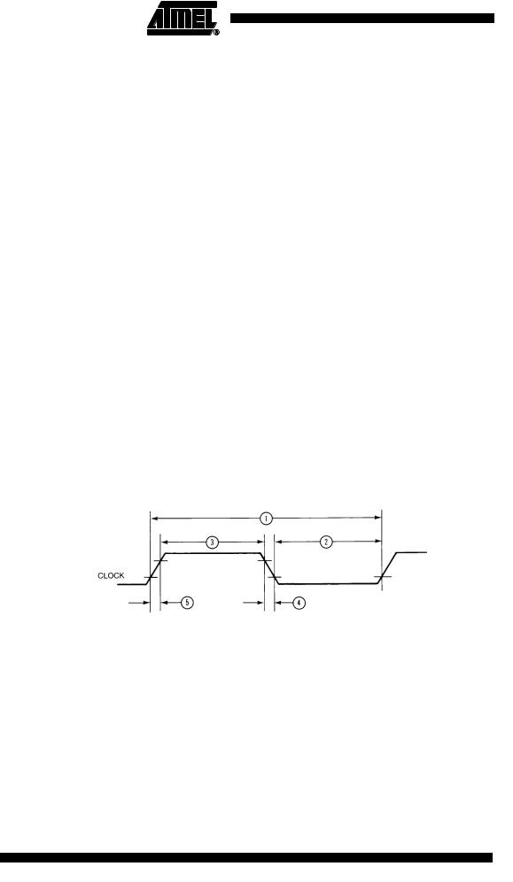
Table 5. Static Characteristics
VCC = 5.0 VDC ± 10%; GND = 0 VDC; Tc = -55/+125°C or -40/+85°C
Symbol |
Parameter |
|
|
Min |
Max |
Unit |
|
|
|
|
|
|
|||
ICC |
Maximum Supply Current (VCC = 5.5V; CLK = fmax; part in Reset) |
|
136 |
mA |
|||
C |
in |
Capacitance (V |
IN |
= 0, T = 25°C, f = 1MHz)(2) |
|
20 |
pF |
|
|
A |
|
|
|
||
CL |
Output Load Capacitance |
|
130 |
pF |
|||
Notes: 1. Test load, see Figure 5.
2. Capacitance is periodically sampled rather than 100% tested.
Dynamic (Switching)
Characteristics
The limits and values given in this section apply over the full case temperature range - 55°C to +125°C and VCC in the range 4.5V to 5.5V, See “AC Electrical Specification Definitions” on page 13.
The numbers (N°) refer to the timing diagrams. See Figure 4, Figure 6, Figure 7, Figure 8 and Figure 9.
Table 6. AC Electrical Characteristics - Clock Input
VCC = 5.0 VDC ± 10%; GND = 0 VDC; Tc = -55°C to +125°C (see Figure 4)
|
|
|
16.67 MHz |
20 MHz |
25 MHz |
33.33 MHz |
|
||||
|
|
|
|
|
|
|
|
|
|
|
|
N° |
Parameter |
Min |
Max |
Min |
Max |
Min |
Max |
Min |
Max |
Unit |
|
|
|
|
|
|
|
|
|
|
|
|
|
|
Frequency of Operation |
8 |
16.67 |
12.5 |
20 |
12.5 |
25 |
16.7 |
33.33 |
MHz |
|
|
|
|
|
|
|
|
|
|
|
|
|
1 |
Clck Time |
60 |
125 |
50 |
80 |
40 |
80 |
30 |
60 |
ns |
|
|
|
|
|
|
|
|
|
|
|
|
|
2, 3 |
Clock Pulse Width |
24 |
95 |
20 |
54 |
15 |
59 |
14 |
66 |
ns |
|
|
|
|
|
|
|
|
|
|
|
|
|
4, 5 |
Rise and Fall Times |
|
5 |
|
5 |
|
4 |
|
3 |
ns |
|
|
|
|
|
|
|
|
|
|
|
|
|
Figure 4. Clock Input Timing Diagram
Note: Timing measurements are referenced to and from a low voltage of 0.8V and a high voltage of 2.0V, unless otherwise noted. The voltage swing through this range should start outside, and pass through, the range such that the rise of fall will be linear between 0.8V and 2.0V.
10 TS68882
2119A–HIREL–04/02
TS68882
Table 7. AC Electrical Characteristics – Read and Write Cycles(1)
VCC = 5.0 VDC ± 10%; GND = 0 VDC; Tc = -55°C/+125°C or Tc = -40°C/+85°C (see Figure 7, Figure 8, Figure 9)
|
|
|
|
|
|
|
|
|
|
|
|
|
|
|
|
|
|
|
|
|
|
|
|
|
|
|
|
|
|
|
|
|
|
|
|
|
|
|
|
|
16.67 MHz |
20 MHz |
25 MHz |
33.33 MHz |
|
||||
|
|
|
|
|
|
|
|
|
|
|
|
|
|||||||||||||||||||||||||||||||||||||
N° |
|
|
Parameter |
Min |
Max |
Min |
Max |
Min |
Max |
Min |
Max |
Unit |
|||||||||||||||||||||||||||||||||||||
|
|
|
|
|
|
|
|
|
|
|
|
|
|
|
|
||||||||||||||||||||||||||||||||||
6 |
|
|
Address valid to |
|
|
asserted(5) |
15 |
|
10 |
|
5 |
|
5 |
|
ns |
||||||||||||||||||||||||||||||||||
AS |
|
|
|
|
|||||||||||||||||||||||||||||||||||||||||||||
6a |
|
Address valid to |
|
|
|
|
asserted (read)(5) |
15 |
|
10 |
|
5 |
|
5 |
|
ns |
|||||||||||||||||||||||||||||||||
DS |
|
|
|
|
|||||||||||||||||||||||||||||||||||||||||||||
6b |
|
Address valid to |
|
|
|
|
asserted (write)(5) |
50 |
|
50 |
|
35 |
|
26 |
|
ns |
|||||||||||||||||||||||||||||||||
DS |
|
|
|
|
|||||||||||||||||||||||||||||||||||||||||||||
7 |
|
|
|
negated to address invalid(6) |
10 |
|
10 |
|
5 |
|
5 |
|
ns |
||||||||||||||||||||||||||||||||||||
|
|
AS |
|
|
|
|
|||||||||||||||||||||||||||||||||||||||||||
7a |
|
|
|
negated to address invalid(6) |
10 |
|
10 |
|
5 |
|
5 |
|
ns |
||||||||||||||||||||||||||||||||||||
DS |
|
|
|
|
|||||||||||||||||||||||||||||||||||||||||||||
|
|
|
|
asserted to |
|
|
|
|
|
|
asserted or |
|
|
asserted |
|
|
|
|
|
|
|
|
|
||||||||||||||||||||||||||
8 |
|
|
CS |
AS |
AS |
0 |
|
0 |
|
0 |
|
0 |
|
ns |
|||||||||||||||||||||||||||||||||||
|
|
|
|
|
|
|
|
|
|
|
|
|
|
|
|
|
|
|
|
|
|
|
|
|
|
|
|
|
|
|
|
|
|
|
|
|
|
|
|
|
|
|
|
||||||
|
|
to CS asserted(9) |
|
|
|
|
|||||||||||||||||||||||||||||||||||||||||||
|
|
|
|
|
|
|
|
|
|
|
|
||||||||||||||||||||||||||||||||||||||
|
|
|
|
asserted to |
|
|
|
|
|
|
|
asserted or |
|
|
|
asserted |
|
|
|
|
|
|
|
|
|
||||||||||||||||||||||||
8a |
|
|
CS |
DS |
DS |
0 |
|
0 |
|
0 |
|
0 |
|
ns |
|||||||||||||||||||||||||||||||||||
|
|
|
|
|
|
|
|
|
|
|
|
|
|
|
|
|
|
|
|
|
|
|
|
|
|
|
|
|
|
|
|
|
|
|
|
|
|
|
|
|
|
|
|
||||||
|
|
to CS asserted (read)(9) |
|
|
|
|
|||||||||||||||||||||||||||||||||||||||||||
|
|
|
|
|
|
|
|
|
|
|
|
||||||||||||||||||||||||||||||||||||||
|
|
|
|
asserted to |
|
|
|
|
|
|
|
asserted or |
|
|
|
asserted |
|
|
|
|
|
|
|
|
|
||||||||||||||||||||||||
8b |
|
|
CS |
DS |
DS |
30 |
|
25 |
|
20 |
|
15 |
|
ns |
|||||||||||||||||||||||||||||||||||
|
|
|
|
|
|
|
|
|
|
|
|
|
|
|
|
|
|
|
|
|
|
|
|
|
|
|
|
|
|
|
|
|
|
|
|
|
|
|
|
|
|
|
|
||||||
|
|
to CS asserted (write)(9) |
|
|
|
|
|||||||||||||||||||||||||||||||||||||||||||
|
|
|
|
|
|
|
|
|
|
|
|
||||||||||||||||||||||||||||||||||||||
9 |
|
|
|
negated to |
|
|
|
|
|
|
|
|
|
negated |
10 |
|
10 |
|
5 |
|
5 |
|
ns |
||||||||||||||||||||||||||
|
|
AS |
CS |
|
|
|
|
||||||||||||||||||||||||||||||||||||||||||
|
|
|
|
|
|
|
|
|
|
|
|
|
|
|
|
|
|
|
|||||||||||||||||||||||||||||||
9a |
|
|
|
negated to |
|
|
|
|
|
|
|
|
negated |
10 |
|
10 |
|
5 |
|
5 |
|
ns |
|||||||||||||||||||||||||||
DS |
CS |
|
|
|
|
||||||||||||||||||||||||||||||||||||||||||||
|
|
|
|
|
|
|
|
|
|
|
|
|
|
|
|
|
|
|
|||||||||||||||||||||||||||||||
10 |
|
|
|
|
high to |
|
|
|
|
|
|
|
|
asserted (read) |
15 |
|
10 |
|
5 |
|
5 |
|
ns |
||||||||||||||||||||||||||
|
R/W |
AS |
|
|
|
|
|||||||||||||||||||||||||||||||||||||||||||
|
|
|
|
|
|
|
|
|
|
|
|
|
|
|
|
|
|
|
|||||||||||||||||||||||||||||||
10a |
|
|
|
|
high to |
|
|
|
|
|
|
|
|
|
asserted (read) |
15 |
|
10 |
|
5 |
|
5 |
|
ns |
|||||||||||||||||||||||||
R/W |
DS |
|
|
|
|
||||||||||||||||||||||||||||||||||||||||||||
|
|
|
|
|
|
|
|
|
|
|
|
|
|
|
|
|
|||||||||||||||||||||||||||||||||
10b |
|
|
|
low to |
|
|
|
|
asserted (write) |
35 |
|
30 |
|
25 |
|
25 |
|
ns |
|||||||||||||||||||||||||||||||
R/W |
DS |
|
|
|
|
||||||||||||||||||||||||||||||||||||||||||||
|
|
|
|
|
|
|
|
|
|
|
|
|
|
|
|
|
|
|
|
|
|
||||||||||||||||||||||||||||
|
|
|
|
|
|
|
|
|
|
|
|
|
|
|
|
|
|
|
|
|
|
|
|
low (read) or |
|
|
|
|
|
|
|
|
|
||||||||||||||||
11 |
|
|
AS |
negated to R/W |
10 |
|
10 |
|
5 |
|
5 |
|
ns |
||||||||||||||||||||||||||||||||||||
|
|
|
|
|
|
|
|
|
|
|
|
|
|
|
|
|
|
|
|
|
|
|
|
|
|
|
|
|
|
|
|
|
|
|
|
|
|
|
|
|
|
|
|
||||||
|
|
AS negated to R/W high (write) |
|
|
|
|
|||||||||||||||||||||||||||||||||||||||||||
|
|
|
|
|
|
|
|
|
|
|
|
||||||||||||||||||||||||||||||||||||||
|
|
|
|
|
|
|
|
|
|
|
|
|
|
||||||||||||||||||||||||||||||||||||
|
|
|
|
negated to R/W low (read) or |
|
|
|
|
|
|
|
|
|
||||||||||||||||||||||||||||||||||||
11a |
|
|
DS |
10 |
|
10 |
|
5 |
|
5 |
|
ns |
|||||||||||||||||||||||||||||||||||||
|
|
DS negated to R/W high (write) |
|
|
|
|
|||||||||||||||||||||||||||||||||||||||||||
|
|
|
|
|
|
|
|
|
|
|
|
||||||||||||||||||||||||||||||||||||||
|
|
|
|
|
|
|
|
|
|
|
|
|
|
||||||||||||||||||||||||||||||||||||
12 |
|
|
|
width asserted (write) |
40 |
|
38 |
|
30 |
|
23 |
|
ns |
||||||||||||||||||||||||||||||||||||
DS |
|
|
|
|
|||||||||||||||||||||||||||||||||||||||||||||
|
|
|
|
|
|
|
|
|
|
|
|
|
|||||||||||||||||||||||||||||||||||||
13 |
|
|
|
width negated |
40 |
|
38 |
|
30 |
|
23 |
|
ns |
||||||||||||||||||||||||||||||||||||
|
DS |
|
|
|
|
||||||||||||||||||||||||||||||||||||||||||||
|
|
|
|
|
|
|
|
|
|
|
|
|
|
|
|
||||||||||||||||||||||||||||||||||
13a |
|
|
|
negated to |
|
|
|
|
|
|
|
|
asserted(4) |
30 |
|
30 |
|
25 |
|
18 |
|
ns |
|||||||||||||||||||||||||||
DS |
AS |
|
|
|
|
||||||||||||||||||||||||||||||||||||||||||||
14 |
|
|
|
|
|
|
asserted to data-out valid (read)(2) |
|
80 |
|
45 |
|
45 |
|
30 |
ns |
|||||||||||||||||||||||||||||||||
|
CS, |
DS |
|
|
|
|
|||||||||||||||||||||||||||||||||||||||||||
15 |
|
|
|
negated to data-out invalid (read) |
0 |
|
0 |
|
0 |
|
0 |
|
ns |
||||||||||||||||||||||||||||||||||||
|
DS |
|
|
|
|
||||||||||||||||||||||||||||||||||||||||||||
|
|
|
|
|
|
|
|
|
|
|
|
|
|
||||||||||||||||||||||||||||||||||||
|
|
|
|
negated to data-out high impedance |
|
|
|
|
|
|
|
|
|
||||||||||||||||||||||||||||||||||||
16 |
|
|
DS |
|
50 |
|
35 |
|
35 |
|
30 |
ns |
|||||||||||||||||||||||||||||||||||||
|
|
(read) |
|
|
|
|
|||||||||||||||||||||||||||||||||||||||||||
|
|
|
|
|
|
|
|
|
|
|
|
||||||||||||||||||||||||||||||||||||||
|
|
|
|
|
|
|
|
|
|
|
|
|
|
|
|||||||||||||||||||||||||||||||||||
17 |
|
|
Data-in invalid to |
|
|
|
asserted (write) |
15 |
|
10 |
|
5 |
|
5 |
|
ns |
|||||||||||||||||||||||||||||||||
|
|
DS |
|
|
|
|
|||||||||||||||||||||||||||||||||||||||||||
|
|
|
|
|
|
|
|
|
|
|
|
|
|
||||||||||||||||||||||||||||||||||||
18 |
|
|
|
negated to data-in invalid (write) |
15 |
|
10 |
|
5 |
|
5 |
|
ns |
||||||||||||||||||||||||||||||||||||
|
DS |
|
|
|
|
||||||||||||||||||||||||||||||||||||||||||||
|
|
|
|
|
|
|
|
|
|
|
|
|
|
|
|
|
|
|
|
|
|
|
|
||||||||||||||||||||||||||
|
|
|
|
|
|
true to |
|
|
|
|
|
|
|
|
|
|
|
|
|
|
|
|
and |
|
|
|
|
|
|
|
|
|
|
|
|
|
|
|
|
|
|
||||||||
19 |
|
|
START |
DSACK0 |
DSACK1 |
|
50 |
|
35 |
|
25 |
|
20 |
ns |
|||||||||||||||||||||||||||||||||||
|
|
asserted(2) |
|
|
|
|
|||||||||||||||||||||||||||||||||||||||||||
|
|
|
|
|
|
|
|
|
|
|
|
||||||||||||||||||||||||||||||||||||||
|
|
|
|
|
|
|
|
|
asserted to |
|
|
|
|
|
asserted |
|
|
|
|
|
|
|
|
|
|||||||||||||||||||||||||
19a |
|
|
DSACK0 |
DSACK1 |
-15 |
15 |
-10 |
10 |
-10 |
10 |
|
5 |
ns |
||||||||||||||||||||||||||||||||||||
|
|
(skew)(7) |
|
||||||||||||||||||||||||||||||||||||||||||||||
|
|
|
|
|
|
|
|
|
|
|
|
||||||||||||||||||||||||||||||||||||||
|
|
|
|
|
|
|
|
or |
|
|
|
|
|
|
|
|
|
|
|
|
|
|
|
|
|
asserted to data-out |
|
|
|
|
|
|
|
|
|
||||||||||||||
20 |
|
|
DSACK0 |
DSACK1 |
|
50 |
|
43 |
|
32 |
|
17 |
ns |
||||||||||||||||||||||||||||||||||||
|
|
valid |
|
|
|
|
|||||||||||||||||||||||||||||||||||||||||||
|
|
|
|
|
|
|
|
|
|
|
|
||||||||||||||||||||||||||||||||||||||
|
|
|
|
|
|
|
|
|
|
|
|
|
|
|
|
|
|
||||||||||||||||||||||||||||||||
|
|
|
|
|
|
false to |
|
|
|
|
|
|
|
|
|
|
|
and |
|
|
|
|
|
|
|
|
|
|
|
|
|
|
|
|
|
||||||||||||||
21 |
|
|
START |
DSACK0 |
DSACK1 |
|
50 |
|
30 |
|
40 |
|
30 |
ns |
|||||||||||||||||||||||||||||||||||
|
|
negated(8) |
|
|
|
|
|||||||||||||||||||||||||||||||||||||||||||
|
|
|
|
|
|
|
|
|
|
|
|
||||||||||||||||||||||||||||||||||||||
11
2119A–HIREL–04/02
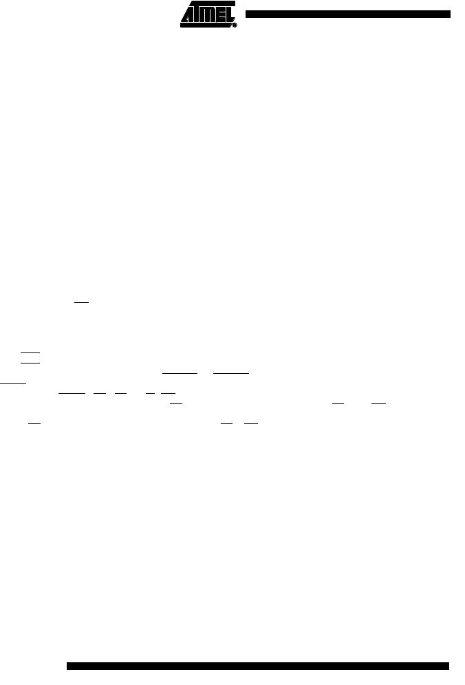
Table 7. AC Electrical Characteristics – Read and Write Cycles(1) (Continued)
VCC = 5.0 VDC ± 10%; GND = 0 VDC; Tc = -55°C/+125°C or Tc = -40°C/+85°C (see Figure 7, Figure 8, Figure 9)
|
|
|
|
|
|
|
|
|
|
|
|
|
|
|
|
16.67 MHz |
20 MHz |
25 MHz |
33.33 MHz |
|
||||
|
|
|
|
|
|
|
|
|
|
|
|
|||||||||||||
N° |
|
Parameter |
Min |
Max |
Min |
Max |
Min |
Max |
Min |
Max |
Unit |
|||||||||||||
|
|
|
|
|
|
|
|
|
|
|
|
|
|
|
|
|
|
|
|
|
||||
|
|
|
false to |
|
|
|
and |
|
|
|
|
|
|
|
|
|
|
|
|
|
||||
22 |
|
START |
DSACK0 |
DSACK1 |
|
70 |
|
55 |
|
55 |
|
40 |
ns |
|||||||||||
|
high impedance(8) |
|
|
|
|
|||||||||||||||||||
|
|
|
|
|
|
|
|
|
|
|
||||||||||||||
|
|
|
true to clock high (synchronous |
|
|
|
|
|
|
|
|
|
||||||||||||
23 |
|
START |
0 |
|
0 |
|
0 |
|
0 |
|
ns |
|||||||||||||
|
read)(3)(8) |
|
|
|
|
|||||||||||||||||||
|
|
|
|
|
|
|
|
|
|
|
||||||||||||||
24 |
|
Clock low to data-out valid synchronous |
|
105 |
|
80 |
|
60 |
|
45 |
ns |
|||||||||||||
|
read)(3) |
|
|
|
|
|||||||||||||||||||
|
|
|
|
|
|
|
|
|
|
|
||||||||||||||
|
|
|
true to data-out valid (synchronous |
0 |
105+ |
|
80 + |
|
60+ |
|
45- |
ns |
||||||||||||
25 |
|
START |
|
|
|
|||||||||||||||||||
|
read)(3)(8) |
1.5 |
2.5 |
1.5 |
2.5 |
1.5 |
2.5 |
1.5 |
2.5 |
Clks |
||||||||||||||
|
|
|||||||||||||||||||||||
|
|
Clock low to |
|
|
|
and |
|
|
|
|
|
|
|
|
|
|
|
|
|
|
||||
26 |
|
DSACK0 |
DSACK1 |
|
75 |
|
55 |
|
45 |
|
30 |
ns |
||||||||||||
|
asserted (synchronous read(3) |
|
|
|
|
|||||||||||||||||||
|
|
|
|
|
|
|
|
|
|
|
||||||||||||||
|
|
|
true to |
|
|
|
and |
|
|
|
|
|
75+ |
|
55+ |
|
45+ |
|
30- |
ns |
||||
27 |
|
START |
DSACK0 |
DSACK1 |
|
|
|
|
||||||||||||||||
|
asserted (synchronous read) (3)(8) |
1.5 |
2.5 |
1.5 |
2.5 |
1.5 |
2.5 |
1.5 |
2.5 |
Clks |
||||||||||||||
|
|
|||||||||||||||||||||||
Notes: 1. Timing measurements are referenced to and from a low voltage of 0.8V and a high voltage of 2.0V, unless otherwise noted. The voltage swing through this range should start outside, and pass through, the range such that the rise or fall will be linear between 0.8V and 2.0V.
2.These specifications only apply if the TS68882 has completed all internal operations initiated by the termination of the previous bus cycle when DS was negated.
3.Synchronous read cycles occur only when the save or response CIR locations are read.
4.This specification only applies to systems in which back-to-back accesses (read-write or write-write) of the operand CIR can occur. When the TS68882 is used as a co-processor to the TS68020/68030, this can occur when the addressing mode is immediate.
5.If the SIZE pin is not strapped to either VCC or GND, it must have the same setup times as do addresses.
6.If the SIZE pin is not strapped to either VCC or GND, it must have the same hold times as do addresses.
7.This number is reduced to 5 nanoseconds if DSACK0 and DSACK1 have equal loads.
8.START is not an external signal; rather, it is the logical condition that indicates the start of an access. The logical equation for this condition is START = CS + AS + (R/W · DS).
9.If a subsequent access is not a FPCP access, CS must be negated before the assertion of AS and/or DS on the non-FPCP access. These specifications replace the old specifications 8 and 8A (the old specifications implied that in all cases, transitions in CS must not occur simultaneously with transitions of AS or DS. This is not a requirement of the TS68882).
12 TS68882
2119A–HIREL–04/02
|
|
|
TS68882 |
|
|
|
|
Test Conditions Specific |
|
||
|
|
||
to the Device |
|
|
|
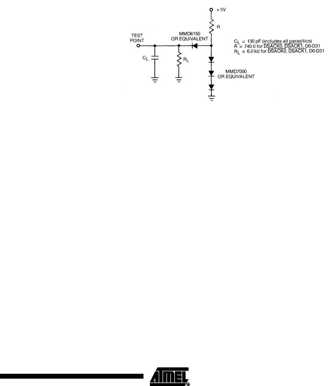
Test Load |
The applicable loading network shall be as defined in column “Test conditions” of Table |
||
|
|
2, referring to the loading network number as shown in Figure 5. |
|
|
|
Figure 5. Test Loads |
|
AC Electrical Specification The AC specifications presented consist of output delays, input setup and hold times, Definitions and signal skew times. All signals are specified relative to an appropriate edge of the
clock input and, possibly, relative to one or more other signals.
The measurement of the AC specifications is defined by the waveforms shown in Figure 6. In order to test the parameters guaranteed inputs must be driven to the voltage levels specified in Figure 6. Outputs are specified with minimum and/or maximum limits, as appropriate, and are measured as shown. Inputs are specified with minimum and, an appropriate maximum setup and hold times, and are measured as shown. Finally, the measurement for signal-to-signal specifications are also shown.
Note that the testing levels used to verify conformance to the AC specifications does not affect the guaranteed DC operation of the device specified in the DC electrical characteristics.
13
2119A–HIREL–04/02
Loading...