


TS68302VR16
Table of contents
 Loading...
ATMEL TS68302VR16, TS68302VA16, TS68302MRB-C16, TS68302MAB-C16, TS68302MA16 Datasheet
...
Features
• TS68000/TS68008 Microprocessor Core Supporting a 16- or 8-bit TS68000 Family
• System Integration Block Including:
– Independent Direct Memory Access (IDMA) Controller
– Interrupt Controller with Two Modes of Operation
– Parallel Input/output (I/O) Ports, some with Interrupt Capability
– On-chip Usable 1152 bytes of Dual-port Random-access Memory (RAM)
– Three Timers, including a Watchdog Timer
– Four Programmable Chip-select Lines with Wait-state Logic
– Programmable Address Mapping of Dual-port RAM and IMP Registers
– On-chip Clock Generator with an Output Clock Signal
–System Control:
System Control Register
Bus Arbitration Logic with Low Interrupt Latency Support
Hardware Watchdog for Monitoring Bus Activity
Low Power (Standby) Modes
Disable CPU Logic (TS68000)
Freeze Control for Debugging Selected On-chip Peripherals
DRAM Refresh Controller
• Communications Processor Including:
– Main Controller (RISC Processor)
– Three Full-duplex Serial Communication Controllers (SCCs)
– Six Serial Direct Memory Access (SDMA) Channels Dedicated to the Three SCCs
– Flexible Physical Interface Accessible by SCCs for Interchip Digital Link (IDL)
General Circuit Interface (GCI, see note), Pulse Code Modulation (PCM), and
Nonmultiplexed Serial Interface (NMSI) Operation
– Serial Communication Port (SCP) for Synchronous Communication, Clock Rate up
to 4.096 MHz
– Serial Management Controllers (SMCs) for IDL and GCI Channels
• Frequency of Operation: 16.67 MHz
• Power Supply: 5 V
± 10%
DC
Integrated
Multiprotocol
Processor (IMP)
TS68302
Description
The IMP is a very large-scale integration (VLSI) device incorporating the main building
blocks needed for the design of a wide variety of controllers. The device is especially
suitable to applications in the communications industry. The IMP is the first device to
offer the benefits of a closely coupled, industry-standard, TS68000/TS68008 microprocessor core and a flexible communications architecture. This multichannel
communications device may be configured to support a number of popular industry
interfaces, including those for the integrated services digital network (ISDN) basic rate
and terminal adapter applications. Through a combination of architectural and programmable features, concurrent operation of different protocols is easily achieved
using the IMP. Data concentrators, line cards, bridges, and gateways are examples of
suitable applications for this versatile device.
The IMP is a high-density complementary metal-oxide semiconductor (HCMOS)
device consisting of a TS68000/TS68008 microprocessor core, a system integration
block (SIB), and a communications processor (CP). The TS68302 block diagram is
shown in Figure 1.
Note: GCI is sometimes referred to as IOM2.
Rev. 2117A–HIREL–11/02
1
Screening/Quality
This product is manufactured in full compliance with either:
• MIL-STD-883 (class B)
• DESC. Drawing 5962-93159
• Or according to Atmel standards
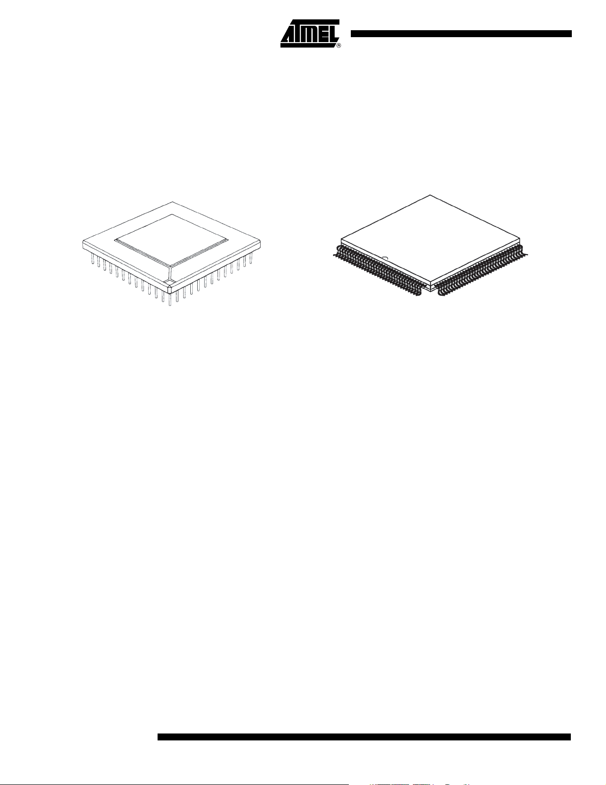
R suffix
PGA 132
(Ceramic Pin Grid Array)
(Ceramic Quad Flat Pack)
A suffix
CERQUAD 132
Introduction The TS68302 integrated multiprotocol processor (IMP) is a very large-scale integration
(VLSI) device incorporating the main building blocks needed for the design of a wide
variety of controllers. The device is especially suitable to applications in the communications industry. The IMP is the first device to offer the benefits of a closely coupled,
industry-standard TS68000 microprocessor core and a flexible communications architecture. The IMP may be configured to support a number of popular industry interfaces,
including those for the Integrated Services Digital Network (ISDN) basic rate and terminal adapter applications. Concurrent operation of different protocols is easily achieved
through a combination of architectural and programmable features. Data concentrators,
line cards, bridges, and gateways are examples of suitable applications for this device.
The IMP is a high-density complementary metal-oxide semiconductor (HCMOS) device
consisting of a TS68000 microprocessor core, a system integration block (SIB), and a
communications processor (CP).
Figure 1 is a block diagram of the TS68302. The processor can be divided into two main
sections: the bus controller and the micromachine. This division reflects the autonomy
with which the sections operate.
2
TS68302
2117A–HIREL–11/02
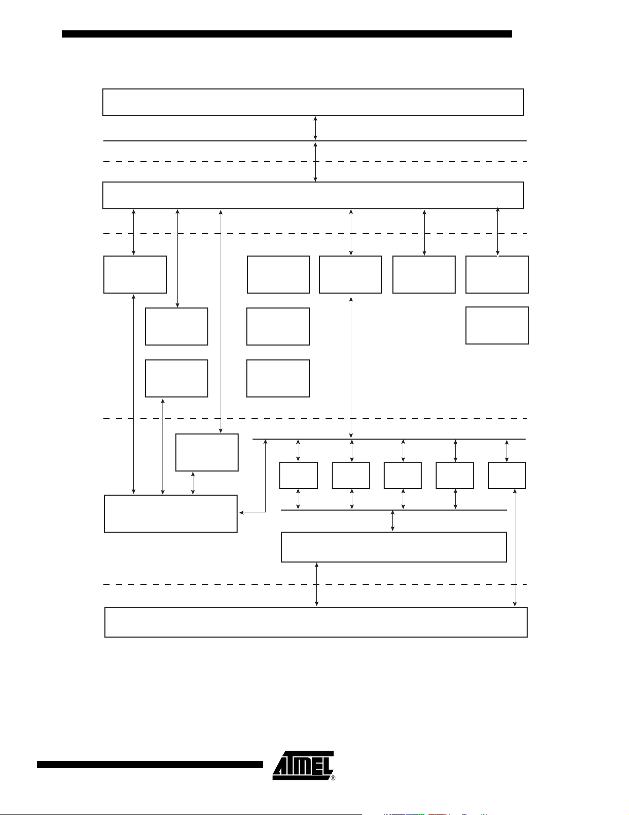
Figure 1. TS68302 Block Diagram
TS68000 BUS
TS68302
TS68000/TS68008 CORE
TS68000/TS68008 CORE
ON-CHIP PERIPHERALS BUS INTERFACE UNIT
INTERRUPT
CONTROLLER
(1 CHANNEL)
CONTROLLER
CONTROLLER
IDMA
DRAM
REFRESH
(6 CHANNELS)
MAIN
(RISC)
SDMA
BUS ARBITER
TIMERS (3)
PARALLEL I/O
PERIPHERAL BUS
SMC (2) SCC1 SCC2 SCC3 SCP
SERIAL CHANNELS PHYSICAL INTERFACE
1152 BYTES
DUAL-PORT
STATIC RAM
CHIP-SELECT
AND WAIT-
STATE LOGIC
SYSTEM INTEGRATION BLOCK
SYSTEM
CONTROL
CLOCK
GENERATOR
2117A–HIREL–11/02
COMMUNICATIONS PROCESSOR
I/O PORTS AND PIN ASSIGNEMENTS
3
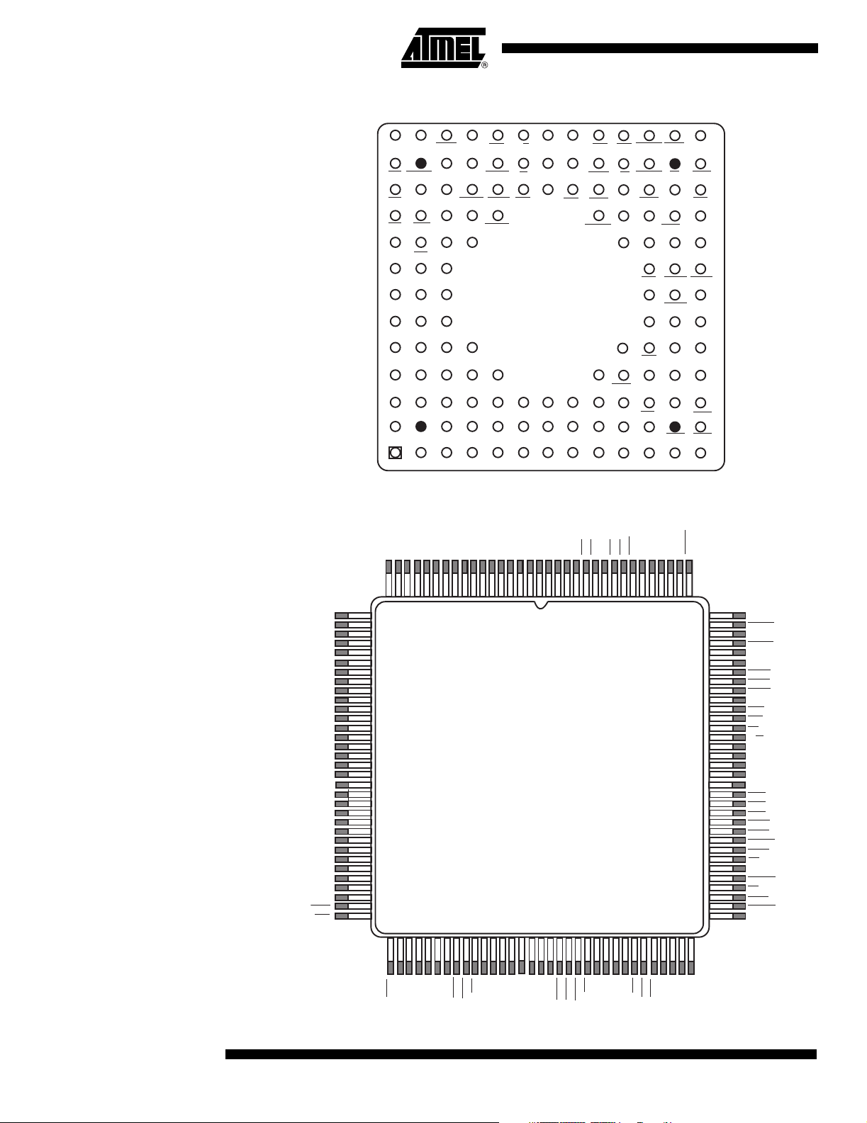
Pin Assignments Figure 2. PGA Terminal Designation
N
M
L
K
J
H
G
F
E
D
C
B
A
PB10 TIN1
CS3 TOUT2
CS2
CS0
FC2
FC0
A1
GND
A6
A7
A10
A11
A14
PB11
RMC
CS1
VDD
A3
A4
A8
GND
A13
A18
A21
IACK1
TIN2
GND
IAC
GND
FC1
A2
A5
A9
A12
A17
A19
A22
GND
VDD
TOUT1
PB9
PB8
VDD
A15
GND
A20
GND
UDS
R/W VDDEXTAL
IACK7
AS CLK0
LDS
IACK6
WDOG
TS68302
BOTTOM VIEW
A16
D14
A23
D13
VDD
D12
D15
12345678910111213
Figure 3. CERQUAD Terminal Designation
GND
XTAL
D11
D10
GND
IPL1 IPL2 RESET HALTRCLK1
IPL0
VDD
D8
D9
BERR BR
AVEC
DTACK
RXD2
TXD2
CTS1
D4 D1
D5
D7
BGACK
NC1
BCLR CD3
VDD
TXD1 BUSW
BRG1
GND
FRZ
PA12
TXD3
CD2
TCLK2 VDD
CD1
D2
D6
GND
BG
RTS3
TCLK1
RTS1
DISCPUNC3
DACK
DONE
GND
DREQ
TCLK3RCLK3
RXD3SDS2
GND
RCLK2
RTS2
CTS3
D0
CTS2
RXD1
D3
VDD
A16
A17
A18
A19
GND
A20
A21
A22
A23
VDD
GND
D15
D14
D13
D12
GND
D11
D10
VDD
GND
CTS3
CD1
A15
A14
A13
A12
GND
A11
A10A9A8A7A6A5A4
17
D9
D8
D7
D6
D5
D4
D3
D2
D1
D0
50
GNDA3A2A1FC0
VDD
FC1
FC2
CS0
CS1
1
68302
CERQUAD132
(window frame down)
Top VIEW
GND
CS2
CS3
RMC
IAC
PB11
PB10
PB9
PB8
117
83
WDOG
GND
TOUT2
TIN2
TOUT1
VDD
TIN1
IACK1
IACK6
IACK7
GND
UDS
LDS
AS
R/W
GND
XTAL
EXTAL
VDD
CLK0
IPL0
IPL1
IPL2
BERR
AVEC
RESET
HALT
BR
NC1
BGACK
BG
BCLR
DTACK
GND
CD2
CTS2
RTS2
VDD
SDS2
TXD3
RXD3
TCLK3
RCLK3
GND
TXD2
RXD2
TCLK2
RCLK2
GND
CTS1
RXD1
4
TS68302
PA12
DACK
DREQ
FRZ
DONE
NC3
BUSW
DISCPU
CD3
BRG1
RTS3
RTS1
TXD1
TCLK1
RCLK1
VDD
2117A–HIREL–11/02
Figure 4. Functional Signal Groups
NMSI1/ISDN I/F
RXD1/L1RXD
TXD1/L1TXD
RCLK1/L1CLK
TCLK1/L1SY0/SDS1
CD1/L1SY1
CTS1/L1RG
RTS1/L1RQ/GCIDCL
BRG2/SDS2/PA7
BRG1
RXD2/PA0
TXD2/PA1
RCLK2/PA2
TCLK2/PA3
CTS2/PA4
RTS2/PA5
CD2/PA6
RXD3/PA8
TXD3/PA9
RCLK3/PA10
TCLK3/PA11
CTS3/SPRXD
RTS3/SPTXD
CD3/SPCLK
BRG3/PA12
DREQ/PA13
DACK/PA14
DONE/PA15
IACK7/PB0
IACK6/PB1
IACK1/PB2
TIN/PB3
TOUT1/PB4
TIN2/PB5
TOUT2/ PB6
WDOG/PB7
PBIO (INTERRUPT)
PB8
PB9
PB10
PB11
NMSI2/PIO
NMSI3/SCP/PIO
IDMA/PAIO
IACK/PBIO
TIMER/PBIO
TS68302
IMP
CLOCKS
ADDRESS BUS
DATA BUS
BUS CONTROL
BUS ARBITRATON
SYSTEM CONTROL
INTERRUPT CONTROL
CHIP SELECT
TESTING
EXTAL
XTAL
CLKO
A23-A1
D15-D0
AS
R/W
UDS/A0
LDS/DS
DTACK
RMC/IOUT1
IAC
BCLR
BR
BG
BGACK
RESET
HALT
BERR
BUSW
DISCPU
IPL0/IRQ1
IPL1/IRQ6
IPL2/IRQ7
FC0
FC1
FC2
AVEC
CS0/IOUT2
CS3-CS1
FRZ
NC(2)
GND(13)
VDD(8)
TS68302
/ IOUT0
2117A–HIREL–11/02
5
Signal Descriptions The input and output signals of the TS68302 are organized into functional groups as
shown in Table 1. Refer to TS68302 Integrated Multiprotocol Processor User’s Manual,
for detailed information on the TS68302 signals.
Table 1. Signal Definitions
Functional Group Signals Number
Clocks XTAL, EXTAL, CLKO 3
System Control RESET
Address Bus A23-A1 23
Data Bus D15-D0 16
Bus Control AS
Bus Control RMC
Bus Arbitration BR
Interrupt Control IPL2-IPL0, FC2-FC0, AVEC 7
NMSI1/ISDN I/F RXD, TXD, RCLK, TCLK, CD
NMSI2/PIO RXD, TXD, RCLK, TCLK, CD
NMSI3/SCP/PIO RXD, TXD, RCLK, TCLK, CD, CTS, RTS, PA12 8
IDMA/PAIO DREQ
IACK/PBIO IACK7
Timer/PBIO TIN2, TIN1, TOUT2, TOUT1, WDOG 5
PBIO PB11-PB8 4
Chip Select CS3
Te st i n g F RZ (2 Spare) 3
V
DD
GND Ground connection 13
, HALT, BERR, BUSW, DISCPU 5
, R/W, UDS/A0, LDS/DS, DTACK 5
, IAC, BCLR 3
, BG, BGACK 3
, CTS, RTS, BRG1 8
, CTS, RTS, SDS2 8
, DACK, DONE 3
, IACK6, IACK1 3
-CS0 4
Power supply 8
Scope This drawing describes the specific requirements for the processor TS68302, 16.67
MHz, in compliance either with MIL-STD-883 class B or with Atmel standards.
Applicable Documents
MIL-STD-883 1. MIL-STD-883: test methods and procedures for electronics.
2. MIL-M-38535: general specifications for microcircuits.
3. Desc Drawing: 5962-93159 (planned).
Requirements
General The microcircuits are in accordance with the applicable document and as specified
herein.
6
TS68302
2117A–HIREL–11/02
TS68302
Design and Construction
Terminal Connections Depending on the package, the terminal connections shall be as shown in Figure 2 and
Figure 3.
Lead Material and Finish Lead material and finish shall be any option of MIL-M-38535.
Package The macrocircuits are packaged in hermetically sealed ceramic packages, which con-
form to case outlines of MIL-M-38535 appendix A (when defined):
• 132-pin Ceramic Pin Grid Array (PGA),
• 132-pin Ceramic Quad Flat Pack (CERQUAD).
The precise case outlines are described in Figure 2 and Figure 3.
Electrical Characteristics
Table 2. Absolute Maximum Ratings
Symbol Parameter Min Max Unit
P
P
LP
LP
LP
D
D
D
D
D
Power Dissipation (typical at 16.67 MHz)
Power Dissipation (typical at 8 MHz)
Low Power Mode Dissipation (typical at 16.67 MHz)
Lowest Power Mode Dissipation (typical at 16.67 MHz)
Lowest Power Mode Dissipation (typical at 50 MHz)
Notes: 1. The values shown are typical. The typical value varies as shown, based on how many IMP on-chip peripherals are enabled
and the rate at which they are clocked.
2. LPREC = 0. Divider = 2.
3. LPREC = 1. Divider = 1024.
4. The stated frequency must be externally applied to EXTAL only after the IMP has been placed in the lowest power mode
with LPREC = 1. The 68000 core is not specified to operate at this frequency, but the rest of the IMP is. In this configuration,
the user does not divide the clock internally using the LPCD4-LPCD0 bits in the system control register.
(1)
(1)
(2)
(3)
(4)
53 64 mA
26 31 mA
36 mA
32 mA
1mA
Unless otherwise stated, all voltages are referenced to the reference terminal (see Table 1).
Table 3. Recommended Condition of Use
Symbol Parameter Min Max Unit
V
CC
V
IL
V
IH
T
case
t
(c) Clock Rise Time - See Figure 5 5 ns
r
tf(c) Clock Fall Time Resistance - Figure 5 5 ns
f
c
t
cyc
2117A–HIREL–11/02
Supply Voltage 4.5 5.5 V
Low Level Input Voltage -0.3 +0.5 V
High Level Input Voltage 2.4 5.5 V
Operating Temperature -55 +125 °C
Clock Frequency - See Figure 5 8 16.67 MHz
Cycle Time - See Figure 5 60 125 ns
7
This device contains protective circuitry to protect the inputs against damage due to high
static voltages or electrical fields; however, it is advised that normal precautions be
taken to avoid application of any voltages higher than maximum-rated voltages to this
high-impedance circuit. Reliability of operation is enhanced if unused inputs are tied to
an appropriate logic voltage level (e.g., either GND or V
DD
).
Figure 5. Clock Input Timing Diagram
t
cyc
2.0V
0.8V
tr (C) tf (C)
Note: Timing measurements are referenced to and from a low voltage of 0.8V and a voltage of 2.0V, unless otherwise noted. The volt-
age swing through this range should start outside, and pass through, the range such that the rise or fall will be linear between
0.8V and 2.0V.
Table 4. Thermal Characteristics at 25°C
Package Symbol Parameter Value Unit
PGA 132 θ
CERQUAD 132 θ
JA
θ
JC
JA
θ
JC
Thermal Resistance - Ceramic Junction To Ambient
Thermal Resistance - Ceramic Junction To Case
Thermal Resistance - Ceramic Junction To Ambient
Thermal Resistance - Ceramic Junction To Case
Power Considerations The average chip-junction temperature, T
= TA + (PD ⋅ θJA) (1)
T
J
T
= Ambient Temperature, °C
A
θ
= Package Thermal Resistance, Junction-to-Ambient, °C/W
JA
P
= P
D
P
INT
P
I/O
Note: For TA = 70°C and PD = 0.5 W at 12.5 MHz Tj = 88°C.
For most applications P
An approximate relationship between P
Solving equations (1) and (2) for K gives:
where K is a constant pertaining to the particular part. K can be determined from equation (3) by measuring P
values of P
value of T
+ P
INT
I/O
= ICC ⋅ VCC, Watts - Chip Internal Power
= Power Dissipation on Input and Output pins - user determined
< 0,30 P
I/O
= K ÷ (TJ + 273) (2)
P
D
K = P
⋅ (TA + 273) + θJA ⋅ PD2 (3)
D
(at equilibrium) for a known TA. Using this value of K, the
and TJ can be obtained by solving equations (1) and (2) iteratively for any
D
.
A
D
and can be neglected.
INT
D
33
5
46
2
, in °C can be obtained from:
J
and TJ (if P
is neglected) is:
I/O
°C/W
°C/W
°C/W
°C/W
8
TS68302
2117A–HIREL–11/02

TS68302
The total thermal resistance of a package (θJA) can be separated into two components,
θ
and θCA, representing the barrier to heat flow from the semiconductor junction to the
JC
package (case), surface (
terms are related by the equation:
θ
= θJC + θCA (4)
JA
θ
is device-related and cannot be influenced by the user. However, θCA is user-depen-
JC
dent and can be minimized by such thermal management techniques as heat sinks,
ambient air cooling and thermal convection. Thus, good thermal management on the
part of the user can significantly reduce
θ
tution of
temperature.
for θJA in equation (1) will result in a lower semiconductor junction
JC
θ
) and from the case to the outside ambient (θCA). These
JC
θ
so that θJA approximately equals θJC. Substi-
CA
Mechanical and Environment
The microcircuits shall meet all mechanical environmental requirements of either MILSTD-883 for class B devices or Atmel standards.
Marking The document that defines the marking is identified in the related reference documents.
Each microcircuit is legible and permanently marked with the following information as
minimum:
• Atmel Logo
• Manufacturer’s part number
• Class B identification
• Date-code of inspection lot
• ESD identifier if available
• Country of manufacturing
Quality Conformance Inspection
DESC/MIL-STD-883 Those quality levels are in accordance with MIL-M-38535 and method 5005 of MIL-
STD-883. Groups A and B inspections are performed on each production lot. Groups C
and D inspection are performed on a periodical basis.
Electrical Characteristics
General Requirements All static and dynamic electrical characteristics specified. For inspection purposes, refer
to relevant specification:
• DESC see “DESC/MIL-STD-883” on page 9
Table 5 and Table 6: Static Electrical Characteristics for all electrical variants. Test
methods refer to IEC 748-2 method number, where existing.
Table 7 and Table 8: Dynamic Electrical Characteristics. Test methods refer to this
specification.
2117A–HIREL–11/02
9
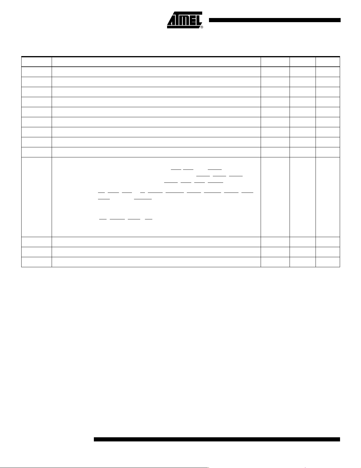
Table 5. DC Electrical Characteristics
= 5.0 Vdc ± 10%; GND = 0 Vdc; Tc = -55°C/+125°C or -40°C/+85°C
V
CC
Symbol Parameter Min Max Unit
V
IH
V
IL
V
CIH
V
CIL
I
IN
C
IN
I
TSI
I
OD
V
OH
V
OL
Input High Voltage (except EXTAL) 2.0 V
DD
V
Input Low Voltage (except EXTAL) VSS - 0.3 0.8 V
Input High Voltage (EXTAL) 4.0 V
DD
V
Input Low Voltage (EXTAL) VSS - 0.3 0.6 V
Input Leakage Current 20 µA
Input Capacitance All Pins 15 pF
Three-state Leakage Current (2.4V/0.5V) 20 µA
Open Drain Leakage Current (2.4V) 20 µA
Output High Voltage (IOH = 400 µA) VDD - 1.0 V
Output Low Voltage
(IOL = 3.2 mA) A1-A23, PB0-PB11, FC0-FC3, CS0-CS3, IAC, AVEC, BG, RCLK1,
RCLK2, RCLK3, TCLK1, TCLK2, TCLK3, RTS1
SDS2, PA12, RXD2, RXD3, CTS2
(I
= 5.3 mA) AS, UDS, LDS, R/W, BERR, BGACK, BCLR, DTACK, DACK, RMC,
OL
, D0-D15, RESET
RMC
, CD2, CD3, DREQ
, RTS2, RTS3,
0.5 V
0.5 V
(IOL = 7.0 mA) TXD1, TXD2, TXD3 0.5 V
(IOL = 8.9 mA) BR, DONE, HALT, (BR as output) 0.5 V
(I
= 3.2 mA) CLKO 0.4 V
OL
O
CLK
O
GCI
O
ALL
Output Drive CLKO 50 pF
Output Drive ISDN I/F (GCI mode) 150 pF
Output Drive All Other Pins 130 pF
10
TS68302
2117A–HIREL–11/02
TS68302
Table 6. DC Electrical Characteristics - NMSI1 in IDL mode
Symbol Parameter Condition Min Nom Max Unit
V
V
Power 4.5 5.0 5.5 V
DD
Common 0 0 0 V
SS
T Temperature Operating range -55 25 +125 °C
Input Pin Characteristics: L1CLK, L1SY1, L1R x D, L1GR
V
V
I
IH
I
IH
Input Low Level Voltage (% of VDD) -10% +20% V
IL
Input High Level Voltage VDD - 20% VDD + 10% V
IH
Input Low Level Current Vin = V
Input High Level Current Vin = V
SS
DD
±10 µA
±10 µA
Output Pin Characteristics: L1T x D, SDS1-SDS2, L1RQ
V
OL
V
OH
Output Low Level Voltage IOL = 2.0 mA 0 0.50 V
Output High Level Voltage IOH = 2.0 mA VDD - 0.5 V
DD
V
2117A–HIREL–11/02
11
Dynamic (Switching) Characteristics
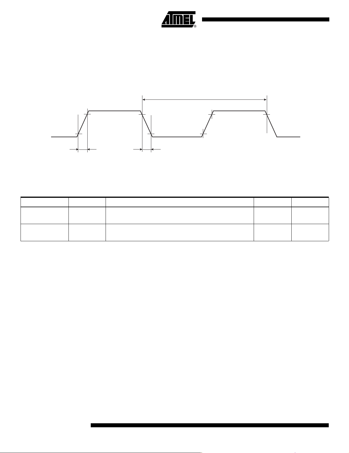
Figure 6. Clock Timing Diagram
V
= 4V
CIH
EXTAL
V
= 0.6V
CIL
The limits and values given in this section apply over the full case temperature range 55°C to +125°C or -40°C to +85°C depending on selection see “Ordering Information”
on page Reference 2 and VCC in the range 4.5V to 5.5V V
= 0.5V and VIH = 2.4V.
IL
The INTERVAL numbers (NUM) refer to the timing diagrams. See Figure 6 to Figure 25.
The AC specifications presented consist of output delays, input setup and hold times,
and signal skew times. All signals are specified relative to an appropriate edge of the
clock (CLKO pin) and possibly to one or more other signals.
1
2
3
5
4
5a
CLKO
5a
Table 7. AC Electrical Specifications - Clock Timing (see Figure 7)
Num. Symbol Parameter Min Max Unit
f Frequency of Operation 8 16.67 MHz
1t
2, 3 t
4, 5 t
5a t
Notes: 1. CLKO loading is 50 pF max.
2. CLKO skew from the rising and falling edges of EXTAL will not differ from each other more than 1 ns, if the EXTAL rise time
cyc
, t
CL
CH
, t
Cr
Cf
CD
equals the EXTAL fall time.
Clock Period (EXTAL) 60 125 ns
Clock Pulse Width (EXTAL) 25 62.5 ns
Clock Rise and Fall Times (EXTAL) 5 ns
EXTAL to CLKO delay
(1)(2)
211ns
12
TS68302
2117A–HIREL–11/02
TS68302
Table 8. AC Electrical Specifications
IMP Bus Master Cycles (see Figure 7, Figure 8 and Figure 9) f = 16.67 MHz
Num. Symbol Parameter Min Max Unit
6t
7t
8t
9t
11 t
12 t
13 t
14 t
14A t
15 t
16 t
17 t
18 t
20 t
20A t
21 t
22 t
23 t
25 t
26 t
27 t
28 t
29 t
30 t
31 t
32 t
33 t
34 t
35 t
36 t
37 t
37A t
38 t
39 t
CHFCADV
CHADZ
CHAFI
CHSL
AFCVSL
CLSH
SHAFI
SL
DSL
SH
CHCZ
SHRH
CHRH
CHRL
ASRV
AFCVRL
RLSL
CLDO
SHDOI
DOSL
DICL
SHDAH
SHDII
SHBEH
DALD I
, t
RHr
RHf
CHGL
CHGH
BRLGL
BRHGH
GALGH
GALBRH
GLZ
GH
Clock high to FC, address valid 45 ns
Clock high to address, data bus high impedance (maximum) 50 ns
Clock high to address, FC invalid (minimum) 0 ns
Clock high to AS, DS asserted
Address, FC valid to AS, DS asserted (read)/AS asserted
(2)
(write)
Clock low to AS, DS negated
AS, DS negated to address, FC invalid
AS (and DS read) width asserted
DS width asserted, write
AS, DS width negated
(2)
(1)
330ns
15 ns
(1)
(2)
(2)
(2)
15 ns
120 ns
60 ns
30 ns
60 ns
Clock high to control bus high impedance 50 ns
AS, DS negated to R/W invalid
Clock high to R/W high
Clock high to R/W low
(1)
(1)
AS asserted to R/W low (write)
Address FC valid to R/W low (write)
R/W low to DS asserted (write)
(2)
(2)(3)
(2)
15 ns
30 ns
30 ns
10 ns
(2)
15 ns
30 ns
Clock low to data-out valid 30 ns
AS, DS, negated to data-out invalid (write)
Data-out valid to DS asserted (write)
Data-in valid to clock low (Setup time on read)
AS, DS negated to DTACK negated (asynchronous hold)
(2)
(2)
(4)
(2)
15 ns
15 ns
7ns
0 110 ns
AS, DS negated to data-in invalid (hold time on read) 0 ns
AS, DS negated to BEER negated 0 ns
DTACK asserted to data-in valid (setup time)
(2)(4)
50 ns
HALT and RESET input transition time 150 ns
Clock high to BG asserted 30 ns
Clock high to BG negated 30 ns
BR asserted to BG asserted 2.5 4.5 clks
BR negated to BG negated
(5)
1.5 2.5 clks
BGACK asserted to BG negated 2.5 4.5 clks
BGACK asserted to BG negated
BG asserted to control, address, data bus high impedance
negated)
(AS
(6)
10 1.5 ns/clks
50 ns
BG width negated 1.5 clks
2117A–HIREL–11/02
13
Table 8. AC Electrical Specifications
IMP Bus Master Cycles (see Figure 7, Figure 8 and Figure 9) f = 16.67 MHz (Continued)
Num. Symbol Parameter Min Max Unit
44 t
46 t
47 t
48 t
53 t
55 t
56 t
57 t
57A t
58 f
58A t
60 t
61 t
62 t
63 t
64 t
SHVPH
GAL
ASI
BELDAL
CHDOI
RLDBD
HRPW
GASD
GAFD
RHSD
RHFD
CHBCL
CHBCH
CLRML
CHRMH
RMHGL
AS, DS negated to AVEC negated 0 50 ns
BGACK width low 1.5 clks
Asynchronous input setup time
BERR asserted to DTACK asserted
(4)
(2)(7)
10 ns
10 ns
Data-out hold from clock high 0 ns
R/W asserted to data bus impedance change 0 ns
HALT/RESET pulse width
(8)
10 clks
BGACK negated to AS, DS, R/W driven 1.5 clks
BGACK negated to FC 1 clks
BR negated to AS, DS, R/W driven
BR negated to FC
(5)
(5)
1.5 clks
1clks
Clock high to BCLR asserted 30 ns
Clock high to BCLR negated
(9)
30 ns
Clock low (S0 falling edge during read) to RMC asserted 30 ns
Clock high (S7 rising edge during write) to RMC negated 30 ns
RMC negated to BG asserted
(10)
30 ns
Notes: 1. For loading capacitance of less than or equal to 50 pF, subtract 4 ns from the value given in the maximum columns.
2. Actual value depends on clock period.
3. When AS and R/W are equally loaded (±20%), subtract 5 ns from the values given in these columns.
4. If the asynchronous input setup (#47) requirement is satisfied for DTACK
, the DTACK asserted to data setup time (#31)
requirement can be ignored. The data must only satisfy the data-in to clock low setup time (#27) for the following clock cycle.
5. The TS68302 will negate BG and begin driving the bus if external arbitration logic negates BR before asserting BGACK.
6. The minimum value must be met to guarantee proper operation. If the maximum value is exceeded, BG may be reasserted.
7. If #47 is satisfied for both DTACK
and BERR, #48 may be ignored. In the absence of DTACK, BERR is a synchronous input
using the asynchronous input setup time (#47).
8. For power-up, the TS68302 must be held in the reset state for 100 ms to allow stabilization of on-chip circuit. After the system is powered up #56 refers to the minimum pulse width required to reset the processor.
9. Occurs on S0 of SDMA read/write access when the SDMA becomes bus master.
10. This specification is valid only when the RMCST bit is set in the SCR register.
14
TS68302
2117A–HIREL–11/02
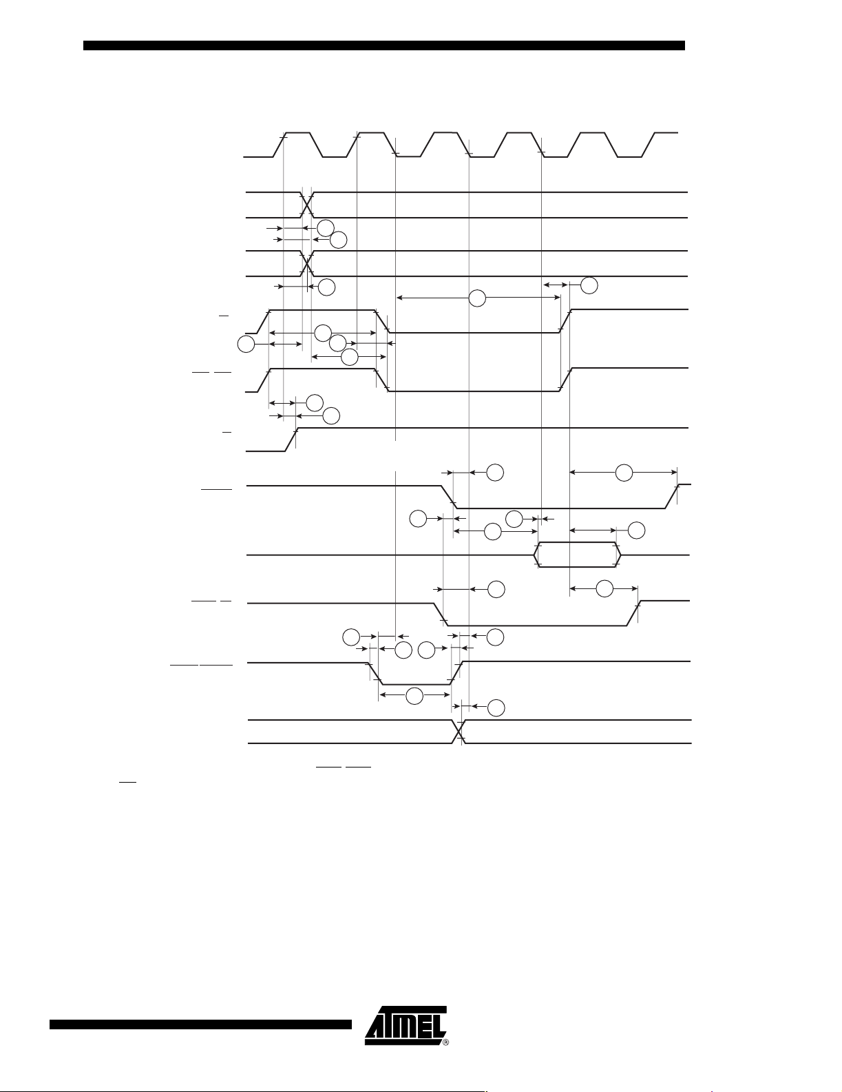
Figure 7. Read Cycle Timing Diagram
CLKO
FC2-FC0
A23-A1
S0 S1 S2 S3 S4 S5 S6
8
6
TS68302
S7
AS
LDS-UDS
R/W
DTACK
DATA IN
BERR/BR
(Note 2)
HALT / RESET
7
13
15
9
11
17
18
48
47 47
32
32
14
47
27
31
47
12
28
29
30
56
ASYNCHRONOUS
INPUTS (Note 1)
47
Notes: 1. Setup time for asynchronous inputs IPL2-IPL0 guarantees their recognition at the next falling edge of the clock.
needs to fall at this time only to ensure being recognized at the end of the bus cycle.
2. BR
3. Timing measurements are reinforced to and from a low voltage of 0.8V and a high voltage of 2.0V, unless otherwise noted.
The voltage swing through this range should start outside and pass through the range such that the rise or fall is linear
between 0.8V and 2.0V.
2117A–HIREL–11/02
15
Loading...