


ATMEL TS68020VF16, TS68020MRB-C25, TS68020MRB-C20, TS68020MRB-C16, TS68020MR25 Datasheet
...Features
•Object Code Compatible with Earlier TS68000 Microprocessors
•Addressing Mode Extensions for Enhanced Support of High Level Languages
•New Bit Field Data Type Accelerates Bit-oriented Application, i.e. Video Graphics
•Fast on-chip Instruction Cache Speed Instructions and Improves Bus Bandwidth
•Co-processor Interface to Companion 32-bit Peripherals: TS68881 and TS68882 Floating Point Co-processors
•Pipelined Architecture with High Degree of Internal Parallelism Allowing Multiple Instructions to be Executed Concurrently
•High Performance Asynchronous Bus in Non-multiplexed and Full 32 Bits
•Dynamic Bus Sizing Efficiently Supports 8-, 16-, 32-bit Memories and Peripherals
•Full Support of Virtual Memory and Virtual Machine
•Sixteen 32-bit General-purpose Data and Address Registers
•Two 32-bit Supervisor Stack Pointers and 5 Special Purpose Control Registers
•18 Addressing Modes and 7 Data Types
•4-Gbyte Direct Addressing Range
•Processor Speed: 16.67 MHz - 20 MHz - 25 MHz
•Power Supply: 5.0 VDC ± 10%
Description
The TS68020 is the first full 32-bit implementation of the TS68000 family of microprocessors. Using HCMOS technology, the TS68020 is implemented with 32-bit registers and data paths, 32-bit addresses, a rich instruction set, and versatile addressing modes.
Screening/Quality
This product is manufactured in full compliance with either:
•MIL-STD-883 (class B)
•DESC 5962 - 860320
•or according to Atmel standards See “Ordering Information” on page 43. Pin connection: see page 3.
R suffix |
F suffix |
|||
PGA 114 |
CQFP 132 |
|||
Ceramic Pin Grid Array |
Ceramic Quad Flat Pack |
|||
|
|
|
|
|
|
|
|
|
|
|
|
|
|
|
HCMOS 32-bit |
Virtual Memory |
Microprocessor |
TS68020 |
Rev. 2115A–HIREL–07/02 |
1 |
Introduction
The TS68020 is a high-performance 32-bit microprocessor. It is the first microprocessor to have evolved from a 16-bit machine to a full 32-bit machine that provides 32-bit address and data buses as well as 32-bit internal structures. Many techniques were utilized to improve performance and at the same time maintain compatibility with other processors of the TS68000 Family. Among the improvements are new addressing modes which better support high-level language structures, an expanded instruction set which provides 32-bit operations for the limited cases not supported by the TS68000 and several new instructions which support new data types. For special-purpose applications when a general-purpose processor alone is not adequate, a co-processor interface is provided.
The TS68020 is a high-performance microprocessor implemented in HCMOS, low power, small geometry process. This process allows CMOS and HMOS (high density NMOS) gates to be combined on the same device. CMOS structures are used where speed and low power is required, and HMOS structures are used where minimum silicon area is desired. This technology enables the TS68020 to be very fast while consuming less power (less than 1.5 watts) and still have a reasonably small die size. It utilizes about 190.000 transistors, 103.000 of which are actually implemented. The package is a pin-grid array (PGA) with 114 pins, arranged 13 pins on a side with a depopulated center and 132 pins ceramic quad flat pack.
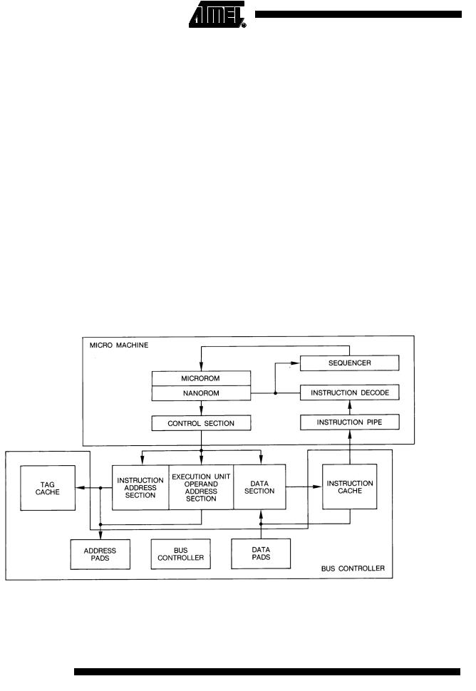
Figure 1 is a block diagram of the TS68020. The processor can be divided into two main sections: the bus controller and the micromachine. This division reflects the autonomy with which the sections operate.
Figure 1. TS68020 Block Diagram
The bus controller consists of the address and data pads and multiplexers required to support dynamic bus sizing, a macro bus controller which schedules the bus cycles on the basis of priority with two state machines (one to control the bus cycles for operated accesses and the other to control the bus cycles for instruction accesses), and the instruction cache with its associated control.
2 TS68020
2115A–HIREL–07/02

TS68020
The micromachine consists of an execution unit, nanorom and microrom storage, an instruction decoder, an instruction pipe, and associated control sections. The execution unit consists of an address section, an operand address section, and a data section. Microcode control is provided by a modified two-level store of microrom and nanorom. Programmed logical arrays (PLAs) are used to provide instruction decode and sequencing information. The instruction pipe and other individual control sections provide the secondary decode of instructions and generated the actual control signals that result in the decoding and interpretation of nanorom and micorom information.
Figure 2. PGA Terminal Designation
Figure 3. CQFP Terminal Designation
3
2115A–HIREL–07/02
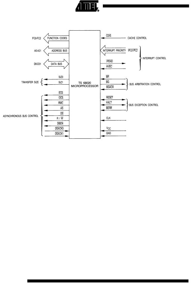
Figure 4. Functional Signal Groups
Signal Description
Figure 4 illustrates the functional signal groups and Table 1 lists the signals and their function.
The VCC and GND pins are separated into four groups to provide individual power supply connections for the address bus buffers, data bus buffers, and all other output buffers and internal logic.
Group |
VCC |
GND |
Address Bus |
A9, D3 |
A10, B9,C3, F12 |
|
|
|
Data Bus |
M8, N8, N13 |
L7, L11, N7, K3 |
|
|
|
Logic |
D1, D2, E3, G11, G13 |
G12, H13, J3, K1 |
|
|
|
Clock |
— |
B1 |
|
|
|
4 TS68020
2115A–HIREL–07/02

TS68020
Table 1. Signal Index
Signal Name |
|
|
|
|
Mnemonic |
|
Function |
|||||||||||||||||||
|
|
|
|
|
|
|
|
|||||||||||||||||||
Address Bus |
|
|
|
|
A0-A31 |
|
32-bit Address Bus Used to address any of 4, 294, 967, 296 bytes. |
|||||||||||||||||||
|
|
|
|
|
|
|
|
|||||||||||||||||||
Data Bus |
|
|
|
|
D0-D31 |
|
32-bit Data Bus Used to Transfer 8, 16, 24 or 32 bits of Data Per Bus Cycle. |
|||||||||||||||||||
|
|
|
|
|
|
|
||||||||||||||||||||
Function Codes |
|
|
|
FC0-FC2 |
|
3-bit Function Case Used to Identify the Address Space of Each Bus Cycle. |
||||||||||||||||||||
|
|
|
|
|
|
|
|
|||||||||||||||||||
Size |
|
|
|
|
SIZ0/SIZ1 |
|
Indicates the Number of Bytes Remaining to be Transferred for this Cycle. |
|||||||||||||||||||
|
|
|
|
|
|
|
|
|
|
|
|
|
|
|
|
|
|
|
|
|
|
|
|
|
|
These Signals, Together with A0 And A1, Define the Active Sections of the |
|
|
|
|
|
|
|
|
|
|
|
|
|
|
|
|
|
|
|
|
|
|
|
|
|
|
Data Bus. |
|
|
|
|
|
|
|
|
|
|
|
|
|
|
|
|
|
|
|
|
|
|
|
|
|
|
|
Read-Modify-Write Cycle |
|
|
|
|
|
|
|
|
|
|
|
|
|
|
|
|
|
|
|
|
|
|
|
|
|
Provides an Indicator that the Current Bus Cycle is Part of an Indivisibleread- |
RMC |
||||||||||||||||||||||||||
|
|
|
|
|
|
|
|
|
|
|
|
|
|
|
|
|
|
|
|
|
|
|
|
|
|
modify-write Operation. |
|
|
|
|
|
|
|
|
|
|
|
|
|
|
|
|
|
|
|
|
|
|
|
|
|
|
|
External Cycle Start |
|
|
|
|
|
|
|
|
|
|
|
|
|
|
|
|
|
|
|
|
|
|
|
|
Provides an Indication that a Bus Cycle is Beginning. |
|
ECS |
||||||||||||||||||||||||||
|
|
|
|
|
|
|
|
|
|
|
|
|
|
|
|
|
|
|
|
|
|
|
|
|||
Operand Cycle Start |
|
|
|
|
|
|
|
|
|
|
|
|
|
|
|
|
|
|
|
|
|
|
|
|
Identical Operation to that of ECS Except that OCS Is Asserted Only During |
|
|
OCS |
|||||||||||||||||||||||||
|
|
|
|
|
|
|
|
|
|
|
|
|
|
|
|
|
|
|
|
|
|
|
|
|
|
the First Bus Cycle of an Operand Transfer. |
|
|
|
|
|
|
|
|
|
|
|
|
|
|
|
|
|
|
|
|
|
|
|
|
|||
Address Strobe |
|
|
|
|
|
|
|
|
|
|
|
|
|
|
|
|
|
|
|
|
|
|
Indicates that a Valid Address is on The Bus. |
|||
|
AS |
|||||||||||||||||||||||||
|
|
|
|
|
|
|
|
|
|
|
|
|
|
|
|
|
|
|
|
|
|
|||||
Data Strobe |
|
|
|
|
|
|
|
|
|
|
|
|
|
|
|
|
|
|
|
|
|
|
Indicates that Valid Data is to be Placed on the Data Bus by an External |
|||
|
DS |
|||||||||||||||||||||||||
|
|
|
|
|
|
|
|
|
|
|
|
|
|
|
|
|
|
|
|
|
|
|
|
|
|
Device or has been Laced on the Data Bus by the TS68020. |
|
|
|
|
|
|
|
|
|
|
|
|
|
|
|
|
|
|
|
|
|||||||
Read/Write |
|
|
|
|
|
|
|
|
|
|
|
|
|
|
|
|
|
|
|
|
|
|
Defines the Bus Transfer as an MPU Read or Write. |
|||
|
|
|
R/W |
|||||||||||||||||||||||
|
|
|
|
|
|
|
|
|
|
|
|
|
|
|
|
|
||||||||||
Data Buffer Enable |
|
|
|
|
|
|
|
|
|
|
|
|
|
|
|
|
|
|
|
|
|
|
|
Provides an Enable Signal for External Data Buffers. |
||
DBEN |
||||||||||||||||||||||||||
|
|
|
|
|
|
|
|
|
|
|
|
|
|
|
|
|
||||||||||
Data Transfer and Size |
|
|
|
|
|
|
|
|
|
|
|
|
|
|
|
|
|
|
|
|
|
|
|
|
|
Bus Response Signals that Indicate the Requested Data Transfer Operation |
|
|
|
DSACK0/DSACK1 |
|||||||||||||||||||||||
Acknowledge |
|
|
|
|
|
|
|
|
|
|
|
|
|
|
|
|
|
|
|
|
|
|
|
|
|
is Completed. In Addition, these Two Lines Indicate the Size of the External |
|
|
|
|
|
|
|
|
|
|
|
|
|
|
|
|
|
|
|
|
|
|
|
|
|
|
Bus Port on a Cycle-by-cycle Basis. |
|
|
|
|
|
|
|
|
|
|
|
|
|
|
|
||||||||||||
Cache Disable |
|
|
|
|
|
|
|
|
|
|
|
|
|
|
|
|
|
|
|
|
Dynamically Disables the On-chip Cache to Assist Emulator Support. |
|||||
|
CDIS |
|||||||||||||||||||||||||
|
|
|
|
|
|
|
|
|
|
|
|
|
|
|
|
|||||||||||
Interrupt Priority Level |
|
|
|
|
|
|
|
|
|
|
- |
|
|
|
|
|
|
|
|
|
|
|
Provides an Encoded Interrupt Level to the Processor. |
|||
|
|
|
IPL0 |
IPL2 |
||||||||||||||||||||||
|
|
|
|
|
|
|
|
|
|
|
|
|
|
|||||||||||||
Autovector |
|
|
|
|
|
|
|
|
|
|
|
|
|
|
|
|
|
|
|
|
|
Requests an Autovector During an Interrupt Acknowledge Cycle. |
||||
|
|
|
|
AVEC |
||||||||||||||||||||||
|
|
|
|
|
|
|
|
|
|
|||||||||||||||||
Interrupt Pending |
|
|
|
|
|
|
|
|
|
|
|
|
|
|
|
|
|
|
|
Indicates that an Interrupt is Pending. |
||||||
IPEND |
||||||||||||||||||||||||||
|
|
|
|
|
|
|
|
|
|
|
|
|
||||||||||||||
Bus Request |
|
|
|
|
|
|
|
|
|
|
|
|
|
Indicates that an External Device Requires Bus Mastership. |
||||||||||||
|
|
|
|
BR |
||||||||||||||||||||||
|
|
|
|
|
|
|
|
|
|
|
||||||||||||||||
Bus Grant |
|
|
|
|
|
|
|
|
|
|
|
|
Indicates that an External Device may Assume Bus Mastership. |
|||||||||||||
|
|
BG |
||||||||||||||||||||||||
|
|
|
|
|
|
|
|
|||||||||||||||||||
Bus Grant Acknowledge |
|
|
|
|
|
|
|
|
|
|
|
|
|
|
|
|
|
|
|
|
|
Indicates that an External Device has Assumed Bus Mastership. |
||||
BGACK |
||||||||||||||||||||||||||
|
|
|
|
|
|
|
|
|||||||||||||||||||
Reset |
|
|
|
|
|
|
|
|
|
|
|
|
|
|
|
|
|
|
|
|
|
System Reset. |
||||
|
|
RESET |
||||||||||||||||||||||||
|
|
|
|
|
|
|
||||||||||||||||||||
Halt |
|
|
|
|
|
|
|
|
|
|
|
|
|
|
|
|
|
Indicates that the Processor Should Suspend Bus Activity. |
||||||||
|
|
HALT |
||||||||||||||||||||||||
|
|
|
|
|
|
|
||||||||||||||||||||
Bus Error |
|
|
|
|
|
|
|
|
|
|
|
|
|
|
|
|
|
|
|
Indicates an Invalid or Illegal Bus Operation is Being Attempted. |
||||||
|
BERR |
|||||||||||||||||||||||||
|
|
|
|
|
|
|
|
|||||||||||||||||||
Clock |
|
|
|
|
CLK |
|
Clock Input to the Processor. |
|||||||||||||||||||
|
|
|
|
|
|
|
|
|||||||||||||||||||
Power Supply |
|
|
|
|
VCC |
|
+5-volt ± 10% Power Supply. |
|||||||||||||||||||
Ground |
|
|
|
GND |
|
Ground Connection. |
||||||||||||||||||||
|
|
|
|
|
|
|
|
|
|
|
|
|
|
|
|
|
|
|
|
|
|
|
|
|
|
|
5
2115A–HIREL–07/02

Detailed
Specifications
Scope
Applicable
Documents
This drawing describes the specific requirements for the microprocessor 68020, 16.67 MHz, 20 MHz and 25 MHz, in compliance with the MIL-STD-883 class B.
MIL-STD-883
•MIL-STD-883: Test Methods and Procedures for Electronics
•MIL-PRF-38535 appendix A: General Specifications for Microcircuits
•Desc Drawing 5962 - 860320xxx
Requirements
General
Design and Construction
The microcircuits are in accordance with the applicable document and as specified herein.
Terminal Connections |
Depending on the package, the terminal connections shall be as shown in Figure 2 and |
|
Figure 3. |
Lead Material and Finish |
Lead material and finish shall be any option of MIL-STD-1835. |
Package |
The macrocircuits are packages in hermetically sealed ceramic packages which are |
|
conform to case outlines of MIL-STD-1835 (when defined): |
|
• 114-pin SQ.PGA UP PAE Outline |
|
• 132-pin Ceramic Quad Flat Pack CQFP |
|
The precise case outlines are described on Figure 23 and Figure 24. |
6 TS68020
2115A–HIREL–07/02

TS68020
Electrical Characteristics
Table 2. Absolute Maximum Ratings
Symbol |
Parameter |
Test Conditions |
Min |
Max |
Unit |
|
|
|
|
|
|
|
|
VCC |
Supply Voltage |
|
-0.3 |
+7.0 |
V |
|
VI |
Input Voltage |
|
-0.5 |
+7.0 |
V |
|
|
|
|
|
|
|
|
Pdmax |
Max Power Dissipation |
Tcase = -55°C |
|
2.0 |
W |
|
|
|
|
|
|||
Tcase = +125°C |
|
1.9 |
W |
|||
|
|
|
||||
Tcase |
Operating Temperature |
M Suffix |
-55 |
+125 |
°C |
|
|
|
|
|
|||
V Suffix |
-40 |
+85 |
°C |
|||
|
|
|||||
|
|
|
|
|
|
|
Tstg |
Storage Temperature |
|
-55 |
+150 |
°C |
|
Tleads |
Lead Temperature |
Max 5 Sec. Soldering |
|
+270 |
°C |
Table 3. Recommended Condition of Use
Unless otherwise stated, all voltages are referenced to the reference terminal (see Table 1).
Symbol |
|
Parameter |
|
Min |
|
Max |
Unit |
|
|
|
|
|
|
|
|
VCC |
|
Supply Voltage |
|
4.5 |
|
5.5 |
V |
VIL |
|
Low Level Input Voltage |
|
-0.3 |
|
0.5 |
V |
VIH |
|
High Level Input Voltage |
|
2.4 |
|
5.25 |
V |
Tcase |
|
Operating Temperature |
|
-55 |
|
+125 |
°C |
RL |
|
Value of Output Load Resistance |
|
(1) |
|
|
Ω |
|
|
|
|
|
|||
|
|
|
|
|
|
|
|
CL |
|
Output Loading Capacitance |
|
|
|
(1) |
pF |
|
|
|
|
|
|||
|
|
|
|
|
|
|
|
|
|
|
68020-16 |
|
|
5 |
|
tr(c)–tf(c) |
|
|
|
|
|
|
|
|
Clock Rise Time (See Figure 5) |
68020-20 |
|
|
5 |
ns |
|
|
|
|
|
|
|
|
|
|
|
|
68020-25 |
|
|
4 |
|
|
|
|
|
|
|
|
|
|
|
|
68020-16 |
8 |
|
16.67 |
|
fc |
|
|
|
|
|
|
|
|
Clock Frequency (See Figure 5) |
68020-20 |
12.5 |
|
20 |
MHz |
|
|
|
|
68020-25 |
12.5 |
|
25 |
|
|
|
|
|
|
|
|
|
|
|
|
68020-16 |
60 |
|
125 |
|
tcyc |
|
|
|
|
|
|
|
|
Cycle Time (see Figure 5) |
68020-20 |
50 |
|
80 |
ns |
|
|
|
|
68020-25 |
40 |
|
80 |
|
|
|
|
|
|
|
|
|
|
|
|
68020-16 |
24 |
|
95 |
|
tW(CL) |
|
|
|
|
|
|
|
|
Clock Pulse Width Low (See Figure 5) |
68020-20 |
20 |
|
54 |
ns |
|
|
|
|
|
|
|
|
|
|
|
|
68020-25 |
19 |
|
61 |
|
|
|
|
|
|
|
|
|
|
|
|
68020-16 |
24 |
|
95 |
|
tW(CH) |
|
|
|
|
|
|
|
|
Clock Pulse Width High (See Figure 5) |
68020-20 |
20 |
|
50 |
ns |
|
|
|
|
68020-25 |
19 |
|
61 |
|
|
|
|
|
|
|
|
|
Note: 1. |
Load network number 1 to 4 as specified (Table 7) gives the maximum loading of the relevant output. |
|
|
||||
7
2115A–HIREL–07/02
This device contains protective circuitry against damage due to high static voltages or electrical fields; however, it is advised that normal precautions be taken to avoid application of any voltages higher than maximum-rated voltages to this high-impedance circuit. Reliability of operation is enhanced if unused inputs are tied to an appropriate logic voltage level (e.g., either GND or VCC).
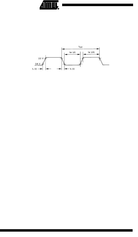
Figure 5. Clock Input Timing Diagram
Note: Timing measurements are referenced to and from a low voltage of 0.8V and a high voltage of 2.0V, unless otherwise noted. The voltage swing through this range should start outside and pass through the range such that the rise or fall will be linear between 0.8V and 2.0V.
Table 4. Thermal Characteristics at 25°C
Package |
Symbol |
Parameter |
Value |
Unit |
|
|
|
|
|
|
|
PGA 114 |
θJA |
Thermal Resistance - Ceramic Junction to Ambient |
26 |
°C/W |
|
θJC |
Thermal Resistance - Ceramic Junction to Case |
5 |
°C/W |
||
|
|||||
CQFP 132 |
θJA |
Thermal Resistance - Ceramic Junction to Ambient |
34 |
°C/W |
|
θJC |
Thermal Resistance - Ceramic Junction to Case |
2 |
°C/W |
||
|
Power Considerations
The average chip-junction temperature, TJ, in °C can be obtained from:
TJ |
= TA + (PD · θ JA) |
(1) |
TA = |
Ambient Temperature, °C |
|
θJA = Package Thermal Resistance, Junction-to-Ambient, °C/W
PD = PINT + PI/O
PINT = ICC · VCC, Watts — Chip Internal Power
PI/O = Power Dissipation on Input and Output Pins — User Determined
For most applications PI/O < PINT and can be neglected.
An approximate relationship between PD and TJ (if PI/O is neglected) is:
PD = K + (TJ + 273) |
|
|
|
(2) |
||
Solving equations (1) and (2) for K gives: |
|
|||||
K = P |
D |
· (T + 273) + θ |
JA |
· P |
2 |
(3) |
|
A |
|
D |
|
||
where K is a constant pertaining to the particular part K can be determined from equation (3) by measuring PD (at equilibrium) for a known TA. Using this value of K, the values of PD and TJ can be obtained by solving equations (1) and (2) iterativley for any value of TA.
8 TS68020
2115A–HIREL–07/02

 TS68020
The total thermal resistance of a package (θJA) can be separated into two components, θJC and θCA, representing the barrier to heat flow from the semiconductor junction to the package (case), surface (θJC) and from the case to the outside ambient (θCA). These terms are related by the equation:
θJA = θJC = θCA |
(4) |
Mechanical and
Environment
Marking
θJC is device related and cannot be influenced by the user. However, θCA is user dependent and can be minimized by such thermal management techniques as heat sinks, ambient air cooling and thermal convection. Thus, good thermal management on the part of the user can significantly reduce θCA so that θJA approximately equals θJC. Substitution of θJC for θJA in equation (1) will result in a lower semiconductor junction temperature.
The microcircuits shall meet all mechanical environmental requirements of MIL-STD- 883 for class B devices.
The document where are defined the marking are identified in the related reference documents. Each microcircuit are legible and permanently marked with the following information as minimum:
•ATMEL Logo
•Manufacturer’s Part Number
•Class B Identification
•Date-code of Inspection Lot
•ESD Identifier if Available
•Country of Manufacturing
Quality Conformance
Inspection
DESC/MIL-STD-883
Is in accordance with MIL-M-38510 and method 5005 of MIL-STD-883. Group A and B inspections are performed on each production lot. Group C and D inspections are performed on a periodical basis.
Electrical
Characteristics
General Requirements
All static and dynamic electrical characteristics specified and the relevant measurement conditions are given below.
(last issue on request to our marketing services).
Table 5: Static electrical characteristics for all electrical variants.
Table 6: Dynamic electrical characteristics for 68020-16 (16.67 MHz), 68020-20 (20 MHz) and 68020-25 (25 MHz).
For static characteristics, test methods refer to “Test Conditions Specific to the Device” on page 14 hereafter of this specification (Table 7).
9
2115A–HIREL–07/02

For dynamic characteristics (Table 6), test methods refer to IEC 748-2 method, where existing.
Indication of “min.” or “max.” in the column “test temperature” means minimum or maximum operating temperature.
.
Table 5. Static Characteristics. VCC = 5.0VDC ± 10%; GND = 0VDC; Tc = -55/+125°C or -40/+85°C (Figure 4 to Figure 8)
Symbol |
|
Parameter |
Condition |
Min |
Max |
Units |
|||||||||||||||||||||||||||||||||||||||
|
|
|
|
|
|
|
|||||||||||||||||||||||||||||||||||||||
ICC |
|
Maximum Supply Current |
VCC = 5.5V |
|
333 |
mA |
|||||||||||||||||||||||||||||||||||||||
|
|
|
|
|
|
|
|
|
|
|
|
|
|
|
|
|
|
|
|
|
|
|
|
|
|
|
|
|
|
|
|
|
|
|
|
|
|
|
|
|
|
Tcase -55°C to +25°C |
|
|
|
ICC |
|
Maximum Supply Current |
VCC = 5.5V |
|
207 |
mA |
|||||||||||||||||||||||||||||||||||||||
|
|
|
|
|
|
|
|
|
|
|
|
|
|
|
|
|
|
|
|
|
|
|
|
|
|
|
|
|
|
|
|
|
|
|
|
|
|
|
|
|
|
Tcase = 125°C |
|
|
|
VIH |
|
High Level Input Voltage |
VO = 0.5V or 2.5 |
2.0 |
VCC |
V |
|||||||||||||||||||||||||||||||||||||||
|
|
|
|
|
|
|
|
|
|
|
|
|
|
|
|
|
|
|
|
|
|
|
|
|
|
|
|
|
|
|
|
|
|
|
|
|
|
|
|
|
|
VCC = 4.5V to 5.5V |
|
|
|
VIL |
|
Low Level Input Voltage |
VO = 0.5V or 2.4V |
-0.5 |
0.8 |
V |
|||||||||||||||||||||||||||||||||||||||
|
|
|
|
|
|
|
|
|
|
|
|
|
|
|
|
|
|
|
|
|
|
|
|
|
|
|
|
|
|
|
|
|
|
|
|
|
|
|
|
|
|
VCC = 4.5V to 5.5V |
|
|
|
VOH |
|
High Level Output Voltage |
IOH = 400 µA |
2.4 |
|
V |
|||||||||||||||||||||||||||||||||||||||
|
|
All Outputs |
|
|
|
|
|||||||||||||||||||||||||||||||||||||||
|
|
|
|
|
|
|
|||||||||||||||||||||||||||||||||||||||
VOL |
|
Low Level Output Voltage |
IOL = 3.2 mA |
|
0.5 |
V |
|||||||||||||||||||||||||||||||||||||||
|
|
Outputs A0-A31, FC0-FC2, D0-D31, SIZ0-SIZ1, |
BG |
|
|
|
Load Circuit as Figure 8 |
|
|
|
|||||||||||||||||||||||||||||||||||
|
|
|
|
|
|
|
|
|
|
|
|
|
|
|
|
|
|
|
|
|
|
|
|
|
|
|
|
|
|
|
|
|
|
|
|
|
|
|
|
|
|
R = 1.22 kΩ |
|
|
|
|
|
|
|
|
|
|
|||||||||||||||||||||||||||||||||||||||
VOL |
|
Low Level Output Voltage |
IOL = 5.3 mA |
|
0.5 |
V |
|||||||||||||||||||||||||||||||||||||||
|
|
Outputs |
|
|
|
|
|
|
|
|
|
|
|
|
|
|
|
|
|
|
|
|
|
|
|
|
|
|
|
|
|
|
|
|
|
|
Load Circuit as Figure 8 |
|
|
|
|||||
|
|
AS, |
DS, |
RMC, |
|
R/W, |
|
|
DBEN, IPEND |
|
|
|
|||||||||||||||||||||||||||||||||
|
|
|
|
|
|
|
|
|
|
|
|
|
|
|
|
|
|
|
|
|
|
|
|
|
|
|
|
|
|
|
|
|
|
|
|
|
|
|
|
|
|
R = 740Ω |
|
|
|
|
|
|
|
|
|
|
|||||||||||||||||||||||||||||||||||||||
VOL |
|
Low Level Output Voltage |
IOL = 2.0 mA |
|
0.5 |
V |
|||||||||||||||||||||||||||||||||||||||
|
|
Outputs |
|
|
|
|
|
|
|
|
|
|
|
|
|
|
|
|
|
|
|
|
|
|
|
|
|
Load Circuit as Figure 8 |
|
|
|
||||||||||||||
|
|
ECS, |
OCS |
|
|
|
|||||||||||||||||||||||||||||||||||||||
|
|
|
|
|
|
|
|
|
|
|
|
|
|
|
|
|
|
|
|
|
|
|
|
|
|
|
|
|
|
|
|
|
|
|
|
|
|
|
|
|
|
R = 2 kΩ |
|
|
|
|
|
|
|
|
|
|
|||||||||||||||||||||||||||||||||||||||
VOL |
|
Low Level Output Voltage |
IOL = 10.7 mA |
|
0.5 |
V |
|||||||||||||||||||||||||||||||||||||||
|
|
Outputs |
HALT, |
|
RESET |
|
|
|
|
|
|
|
|
|
|
|
|
Load Circuit as Figure 6 |
|
|
|
||||||||||||||||||||||||
|
|
|
|
|
|
|
|
|
|
|
|
|
|
|
|
|
|
|
|
|
|
|
|
|
|
|
|
|
|
|
|
|
|
|
|
|
|
|
|
|
|
and Figure 7 |
|
|
|
|
|
|
|
|
|
|
|||||||||||||||||||||||||||||||||||||||
| IIN | |
|
Input Leakage Current (High and Low State) |
-0.5V ≤ VIN ≤ VCC (Max) |
|
2.5 |
µA |
|||||||||||||||||||||||||||||||||||||||
|
|
|
|
|
|
|
|||||||||||||||||||||||||||||||||||||||
| IOHZ | |
|
High level leakage current at three-state outputs |
VOH = 2.4V |
|
2.5 |
µA |
|||||||||||||||||||||||||||||||||||||||
|
|
Outputs A0-A31, |
|
|
|
|
|
|
|
|
|
|
|
|
|
FC0-FC2, |
|
|
|
|
|||||||||||||||||||||||||
|
|
AS, |
DBEN, |
DS, |
D0-D31, R/W, |
|
|
|
|
||||||||||||||||||||||||||||||||||||
|
|
RMC, |
SIZ0-SIZ1 |
|
|
|
|
||||||||||||||||||||||||||||||||||||||
|
|
|
|
|
|
|
|||||||||||||||||||||||||||||||||||||||
| IOLZ | |
|
Low Level Leakage Current at Three-state Outputs |
VOL = 0.5V |
|
2.5 |
µA |
|||||||||||||||||||||||||||||||||||||||
|
|
Outputs A0-A31, |
|
|
|
|
|
|
|
FC0-FC2, |
|
|
|
|
|
|
|||||||||||||||||||||||||||||
|
|
AS, |
DBEN, |
DS, |
D0-D31 R/W, |
RMC, |
|
|
|
|
|||||||||||||||||||||||||||||||||||
|
|
SIZ0-SIZ1 |
|
|
|
|
|||||||||||||||||||||||||||||||||||||||
|
|
|
|
|
|
|
|||||||||||||||||||||||||||||||||||||||
IOS |
|
Output Short-circuit Current |
VCC = 5.5V |
|
200 |
mA |
|||||||||||||||||||||||||||||||||||||||
|
|
(Any Output) |
VO = 0V |
|
|
|
|||||||||||||||||||||||||||||||||||||||
|
|
|
|
|
|
|
|
|
|
|
|
|
|
|
|
|
|
|
|
|
|
|
|
|
|
|
|
|
|
|
|
|
|
|
|
|
|
|
|
|
|
(Pulsed. Duration 1 ms |
|
|
|
|
|
|
|
|
|
|
|
|
|
|
|
|
|
|
|
|
|
|
|
|
|
|
|
|
|
|
|
|
|
|
|
|
|
|
|
|
|
|
|
|
|
Duty Cycle 10:1) |
|
|
|
|
|
|
|
|
|
|
|
|
|
|
|
|
|
|
|
|
|
|
|
|
|
|
|
|
|
|
|
|
|
|
|
|
|
|
|
|
|
|
|
|
|
|
|
|
|
10 TS68020
2115A–HIREL–07/02
 TS68020
Dynamic (Switching)
Characteristics
The limits and values given in this section apply over the full case temperature range - 55°C to +125°C and VCC in the range 4.5V to 5.5V VIL = 0.5V and VIH = 2.4V (See also note 12 and 13). The INTERVAL numbers refer to the timing diagrams. See Figure 5, Figure 9 and Figure 12.
Table 6. Dynamic Electrical Characteristics
|
|
|
|
|
|
|
|
|
|
|
|
|
|
|
|
|
|
|
|
|
|
|
|
|
|
|
|
|
|
|
|
|
|
|
|
|
|
|
|
|
|
|
|
|
|
|
|
|
|
|
Interval |
|
68020-16 |
68020-20 |
68020-25 |
|
|
|||
|
|
|
|
|
|
|
|
|
|
|
|
|
|
|
|
|
|
|
|
|
|
|
|
|
|
|
|
|
|
|
|
|
|
|
|
|
|
|
|
|
|
|
|
|
|
|
|
|
|
|
|
|
|
|
|
|
|
|
|
|
Symbol |
|
Parameter |
Number |
Min |
Max |
Min |
Max |
Min |
Max |
Unit |
Notes |
|||||||||||||||||||||||||||||||||||||||||||||||||
|
|
|
|
|
|
|
|
|
|
|
|
|
||||||||||||||||||||||||||||||||||||||||||||||||
tCPW |
|
Clock Pulse Width |
2 , 3 |
|
24 |
95 |
20 |
54 |
19 |
61 |
ns |
|
||||||||||||||||||||||||||||||||||||||||||||||||
tCHAV |
|
Clock High to Address/FC/Size/RMC |
|
|
|
|
|
|
6 |
|
0 |
30 |
0 |
25 |
0 |
25 |
ns |
|
||||||||||||||||||||||||||||||||||||||||||
|
|
|
|
|
||||||||||||||||||||||||||||||||||||||||||||||||||||||||
|
|
Valid |
|
|
|
|
|
|
|
|
|
|
||||||||||||||||||||||||||||||||||||||||||||||||
|
|
|
|
|
|
|
|
|
|
|
|
|
|
|
|
|
|
|
|
|
|
|
|
|
|
|
|
|
|
|
|
|||||||||||||||||||||||||||||
tCHEV |
|
Clock High to |
|
|
|
|
|
|
|
|
|
|
|
|
|
|
|
|
|
|
|
Asserted |
6A |
0 |
20 |
0 |
15 |
0 |
12 |
ns |
|
|||||||||||||||||||||||||||||
ECS, |
OCS |
|
||||||||||||||||||||||||||||||||||||||||||||||||||||||||||
tCHAZX |
|
|
|
|
|
|
|
|
|
|
|
|
|
|
|
|
|
|
|
|
|
|
|
|
|
|
|
|
|
|
|
|
|
|
|
|
|
|
|
|
|
|
|
|
|
|
|
|
|
|
|
|
|
|
|
|
|
|
|
(11) |
|
Clock High to Address/Data/FC/RMC/ |
7 |
|
0 |
60 |
0 |
50 |
0 |
40 |
ns |
||||||||||||||||||||||||||||||||||||||||||||||||||
|
|
|
||||||||||||||||||||||||||||||||||||||||||||||||||||||||||
|
|
Size High Impedance |
|
|
|
|
|
|
|
|
|
|
||||||||||||||||||||||||||||||||||||||||||||||||
|
|
|
|
|
|
|
|
|
|
|
|
|
|
|
|
|
||||||||||||||||||||||||||||||||||||||||||||
tCHAZn |
|
Clock High to Address/FC/Size/RMC |
|
|
|
|
|
8 |
|
0 |
|
0 |
|
0 |
|
ns |
|
|||||||||||||||||||||||||||||||||||||||||||
|
|
|
|
|
|
|
||||||||||||||||||||||||||||||||||||||||||||||||||||||
|
|
Invalid |
|
|
|
|
|
|
|
|
|
|
||||||||||||||||||||||||||||||||||||||||||||||||
|
|
|
|
|
|
|
|
|
|
|
|
|
|
|
|
|
|
|
|
|
|
|
|
|
|
|||||||||||||||||||||||||||||||||||
tCLSA |
|
Clock Low to |
|
|
|
|
|
|
|
|
|
|
|
|
|
|
|
Asserted |
9 |
|
3 |
30 |
3 |
25 |
3 |
18 |
ns |
|
||||||||||||||||||||||||||||||||
AS, |
|
|
DS |
|
||||||||||||||||||||||||||||||||||||||||||||||||||||||||
tSTSA |
|
|
|
|
|
|
|
|
|
|
|
|
|
|
|
|
|
|
|
|
|
|
|
|
|
|
|
|
|
|
|
|
|
|
|
|
|
|
|
|
|
|
|
|
|
|
|
|
|
|
|
|
|
|
|
|
|
|
|
(1) |
|
AS to DS Assertion (Read)(Skew) |
9A |
-15 |
15 |
-10 |
10 |
-10 |
10 |
ns |
|||||||||||||||||||||||||||||||||||||||||||||||||||
|
|
|||||||||||||||||||||||||||||||||||||||||||||||||||||||||||
tECSA |
|
|
|
|
|
|
|
|
|
Width Asserted |
10 |
|
20 |
|
15 |
|
15 |
|
ns |
|
||||||||||||||||||||||||||||||||||||||||
ECS |
|
|
|
|
||||||||||||||||||||||||||||||||||||||||||||||||||||||||
tOCSA |
|
|
|
|
|
|
|
|
|
Width Asserted |
10A |
20 |
|
15 |
|
15 |
|
ns |
|
|||||||||||||||||||||||||||||||||||||||||
OCS |
|
|
|
|
||||||||||||||||||||||||||||||||||||||||||||||||||||||||
tEOCSN |
|
|
|
|
|
|
|
|
|
|
|
|
|
|
|
|
|
|
|
|
|
|
|
|
|
|
|
|
|
|
|
|
|
|
|
|
|
|
|
|
|
|
|
|
|
|
|
|
|
|
|
|
|
|
|
|
|
|
|
(11) |
|
ECS, OCS Width Negated |
10B |
15 |
|
10 |
|
5 |
|
ns |
|||||||||||||||||||||||||||||||||||||||||||||||||||
|
|
|
|
|
||||||||||||||||||||||||||||||||||||||||||||||||||||||||
|
|
|
|
|
|
|
|
|
|
|
|
|
|
|
|
|
|
|
|
|
|
|
|
|
|
|
|
|
|
|
|
|
|
|
|
|
|
|
|
|
|
|
|
|
|
|
|
|
|
|
11 |
|
15 |
|
10 |
|
6 |
|
ns |
(6) |
tAVSA |
|
Address/FC/Size/RMC Valid to AS |
|
|
|
|
||||||||||||||||||||||||||||||||||||||||||||||||||||||
|
|
|
|
|
|
|||||||||||||||||||||||||||||||||||||||||||||||||||||||
|
|
Asserted (and |
DS |
|
Asserted, Read) |
|
|
|
|
|
|
|
|
|
|
|||||||||||||||||||||||||||||||||||||||||||||
|
|
|
|
|
|
|
|
|
|
|
|
|
|
|
|
|
|
|
|
|
|
|
|
|||||||||||||||||||||||||||||||||||||
tCLSN |
|
Clock Low to |
|
|
|
|
|
|
|
|
|
|
|
|
|
|
|
Negated |
12 |
|
0 |
30 |
0 |
25 |
0 |
15 |
ns |
|
||||||||||||||||||||||||||||||||
AS, |
DS |
|
||||||||||||||||||||||||||||||||||||||||||||||||||||||||||
tCLEN |
|
Clock Low to |
|
|
|
|
|
|
|
|
|
|
|
|
|
|
|
|
|
|
|
|
|
|
|
|
|
|
|
|
|
|
|
12A |
0 |
30 |
0 |
25 |
0 |
15 |
ns |
|
||||||||||||||||||
ECS/OCS Negated |
|
|||||||||||||||||||||||||||||||||||||||||||||||||||||||||||
tSNAI |
|
|
|
|
|
|
|
|
|
|
|
Negated to Address/FC/ |
13 |
|
15 |
|
10 |
|
10 |
|
ns |
|
||||||||||||||||||||||||||||||||||||||
AS, |
DS |
|
|
|
|
|||||||||||||||||||||||||||||||||||||||||||||||||||||||
|
|
|
|
|
|
|
|
|
Invalid |
|
|
|
|
|
|
|
|
|
|
|||||||||||||||||||||||||||||||||||||||||
|
|
Size/RMC |
|
|
|
|
|
|
|
|
|
|
||||||||||||||||||||||||||||||||||||||||||||||||
|
|
|
|
|
|
|
|
|
|
|
|
|
|
|
|
|
|
|
|
|||||||||||||||||||||||||||||||||||||||||
tSWA |
|
|
|
|
|
(and |
|
|
|
|
|
|
Read) Width Asserted |
14 |
|
100 |
|
85 |
|
70 |
|
ns |
|
|||||||||||||||||||||||||||||||||||||
AS |
DS, |
|
|
|
|
|||||||||||||||||||||||||||||||||||||||||||||||||||||||
tSWAW |
|
|
|
|
Width Asserted, Write |
14A |
40 |
|
38 |
|
30 |
|
ns |
|
||||||||||||||||||||||||||||||||||||||||||||||
DS |
|
|
|
|
||||||||||||||||||||||||||||||||||||||||||||||||||||||||
tSN |
|
|
|
|
|
|
|
|
|
|
|
|
|
|
|
|
|
|
|
|
|
|
|
|
|
|
|
|
|
|
|
|
|
|
|
|
|
|
|
|
|
|
|
|
|
|
|
|
|
|
|
|
|
|
|
|
|
|
|
(11) |
|
AS, DS Width Negated |
15 |
|
40 |
|
38 |
|
30 |
|
ns |
||||||||||||||||||||||||||||||||||||||||||||||||||
|
|
|
|
|
|
|||||||||||||||||||||||||||||||||||||||||||||||||||||||
|
|
|
|
|
|
|
|
|
|
|
|
|
|
|
|
|
|
|
|
|
|
|
|
|
|
|
|
|
|
|
|
|
|
|
|
|
|
|
|
|
|
|
|
|
|
|
|
|
|
|
|
|
|
|
|
|
|
|
|
(8) |
tSNSA |
|
DS Negated to AS Asserted |
15A |
35 |
|
30 |
|
25 |
|
ns |
||||||||||||||||||||||||||||||||||||||||||||||||||
|
|
|
|
|
||||||||||||||||||||||||||||||||||||||||||||||||||||||||
|
|
|
|
|
|
|
|
|
|
|
|
|
|
|
|
|
|
|
|
|
|
|
|
|
|
|
|
|
|
|
|
|
|
|
|
|
|
|
|
|
|
|
|
|
|
|
|
|
|
|
|
|
|
|
|
|
|
|
|
(11) |
tCSZ |
|
Clock High to AS/DS/R/W/DBEN High |
16 |
|
|
60 |
|
50 |
|
40 |
ns |
|||||||||||||||||||||||||||||||||||||||||||||||||
|
|
|
|
|
|
|||||||||||||||||||||||||||||||||||||||||||||||||||||||
|
|
Impedance |
|
|
|
|
|
|
|
|
|
|
||||||||||||||||||||||||||||||||||||||||||||||||
|
|
|
|
|
|
|
|
|
|
|
|
|
|
|
|
|
|
|
|
|
|
|
|
|
|
|
|
|
|
|
|
|
|
|
|
|
|
|
|
|
|
|
|
|
|
|
|
|
|
|
|
|
|
|
|
|
|
|
|
|
|
|
|
|
|
|
|
|
|
|
|
|
|
|
|
|
|
|
|
|
|
|
|
|
|
|
|
|
|
|
|
|
|
|
|
|
|
|
|
|
|
|
|
|
|
|
|
|
|
|
|
|
|
|
|
|
|
|
|
|
(6) |
tSNRN |
|
AS, DS Negated to R/W High |
17 |
|
15 |
|
10 |
|
10 |
|
ns |
|||||||||||||||||||||||||||||||||||||||||||||||||
|
|
|
|
|
|
|||||||||||||||||||||||||||||||||||||||||||||||||||||||
tCHRH |
|
|
|
|
|
|
|
|
|
|
|
|
|
|
|
|
|
|
|
|
|
|
|
|
|
|
|
|
|
|
|
High |
18 |
|
0 |
30 |
0 |
25 |
0 |
20 |
ns |
|
||||||||||||||||||
Clock High to R/W |
|
|||||||||||||||||||||||||||||||||||||||||||||||||||||||||||
tCHRL |
|
|
|
|
|
|
|
|
|
|
|
|
|
|
|
|
|
|
|
|
|
|
|
|
|
|
|
|
|
|
|
Low |
20 |
|
0 |
30 |
0 |
25 |
0 |
20 |
ns |
|
||||||||||||||||||
Clock High to R/W |
|
|||||||||||||||||||||||||||||||||||||||||||||||||||||||||||
tRAAA |
|
|
|
|
|
|
|
|
|
|
|
|
|
|
|
|
|
|
|
|
|
|
|
|
|
|
|
|
|
|
|
|
|
|
|
|
|
|
|
|
|
|
|
|
|
|
|
|
|
|
|
|
|
|
|
|
|
|
|
(6) |
|
R/W High to AS Asserted |
21 |
|
15 |
|
10 |
|
5 |
|
ns |
||||||||||||||||||||||||||||||||||||||||||||||||||
|
|
|
|
|
|
|||||||||||||||||||||||||||||||||||||||||||||||||||||||
|
|
|
|
|
|
|
|
|
|
|
|
|
|
|
|
|
|
|
|
|
|
|
|
|
|
|
|
|
|
|
|
|
|
|
|
|
|
|
|
|
|
|
|
|
|
|
|
|
|
|
|
|
|
|
|
|
|
|
|
(6) |
tRASA |
|
R/W Low to DS Asserted (Write) |
22 |
|
75 |
|
60 |
|
50 |
|
ns |
|||||||||||||||||||||||||||||||||||||||||||||||||
|
|
|
|
|
|
|||||||||||||||||||||||||||||||||||||||||||||||||||||||
tCHDO |
|
Clock High to Data Out Valid |
23 |
|
|
30 |
|
25 |
|
25 |
ns |
|
||||||||||||||||||||||||||||||||||||||||||||||||
tSNDI |
|
AS, DS Negated to Data Out Valid |
25 |
|
15 |
|
10 |
|
5 |
|
ns |
(6) |
||||||||||||||||||||||||||||||||||||||||||||||||
|
|
|
|
|
|
|||||||||||||||||||||||||||||||||||||||||||||||||||||||
|
|
|
|
|
|
|
|
|
|
|
|
|
|
|
|
|
|
|
|
|
|
|
|
|
|
|
|
|
|
|
|
|
|
|
|
|
|
|
|
|
|
|
|
|
|
|
|
|
|
|
|
|
|
|
|
|
|
|
|
(9) |
tDNDBN |
|
DS Negated to DBEN Negated (Write) |
25A |
15 |
|
10 |
|
5 |
|
ns |
||||||||||||||||||||||||||||||||||||||||||||||||||
|
|
|
|
|
||||||||||||||||||||||||||||||||||||||||||||||||||||||||
11
2115A–HIREL–07/02

Table 6. Dynamic Electrical Characteristics (Continued)
|
|
|
|
|
|
|
|
|
|
|
|
|
|
|
|
|
|
|
|
|
|
|
|
|
|
|
|
|
|
|
|
|
|
|
|
|
|
|
Interval |
|
68020-16 |
68020-20 |
68020-25 |
|
|
|||
|
|
|
|
|
|
|
|
|
|
|
|
|
|
|
|
|
|
|
|
|
|
|
|
|
|
|
|
|
|
|
|
|
|
|
|
|
|
|
|
|
|
|
|
|
|
|
|
|
Symbol |
|
Parameter |
Number |
Min |
Max |
Min |
Max |
Min |
Max |
Unit |
Notes |
|||||||||||||||||||||||||||||||||||||
|
|
|
|
|
|
|
|
|
|
|
|
|
|
|
|
|
|
|
|
|
|
|
|
|
|
|
|
|
|
|
|
|
|
|
|
|
|
|
|
|
|
|
|
|
|
|
|
|
|
|
|
|
|
|
|
|
|
|
|
|
|
|
|
|
|
|
|
|
|
|
|
|
|
|
|
|
|
|
|
|
|
|
|
|
|
|
|
|
|
|
|
|
|
|
|
|
(6) |
tDVSA |
|
Data Out Valid to DS Asserted (Write) |
26 |
|
15 |
|
10 |
|
5 |
|
ns |
|||||||||||||||||||||||||||||||||||||
|
|
|
|
|
|
|||||||||||||||||||||||||||||||||||||||||||
|
|
26 |
|
|
|
|
|
|
|
|
|
|
|
|
|
|
|
|
|
|
|
|
|
|
|
|
|
|
|
|
|
|
|
|
|
|
|
|
|
|
|
|
|
|
|
|
||
|
|
|
|
|
|
|
|
|
|
|
|
|
||||||||||||||||||||||||||||||||||||
tDICL |
|
Data in Valid to Clock Low (Data Setup) |
27 |
|
5 |
|
5 |
|
5 |
|
ns |
|
||||||||||||||||||||||||||||||||||||
tBELCL |
|
Late |
|
|
|
|
|
|
|
|
|
|
|
|
|
|
|
|
|
|
|
|
|
|
|
|
|
|
|
|
27A |
20 |
|
15 |
|
10 |
|
ns |
|
|||||||||
BERR/HALT Asserted to Clock |
|
|
|
|
||||||||||||||||||||||||||||||||||||||||||||
|
|
Low Setup Time |
|
|
|
|
|
|
|
|
|
|
||||||||||||||||||||||||||||||||||||
|
|
|
|
|
|
|
|
|
|
|
|
|
|
|
|
|
|
|
|
|
|
|
|
|||||||||||||||||||||||||
tSNDN |
|
|
|
|
|
|
|
|
|
|
|
|
|
Negated to |
28 |
|
0 |
80 |
0 |
65 |
0 |
50 |
ns |
|
||||||||||||||||||||||||
AS, |
DS |
|
||||||||||||||||||||||||||||||||||||||||||||||
|
|
|
|
|
|
|
|
|
|
|
|
|
|
|
|
|
|
|
|
|
|
|
|
|
|
|
|
|
|
|
|
|
|
|
|
|
|
|
|
|
||||||||
|
|
DSACKx/BERR/HALT/AVEC Negated |
|
|
|
|
|
|
|
|
|
|
||||||||||||||||||||||||||||||||||||
|
|
|
|
|
|
|
|
|
|
|
|
|
|
|
|
|
|
|
|
|
|
|
|
|
|
|
|
|
|
|
|
|
|
|
|
|
|
|
|
|
|
|
|
|
|
|
|
|
|
|
|
|
|
|
|
|
|
|
|
|
|
|
|
|
|
|
|
|
|
|
|
|
|
|
|
|
|
|
|
|
|
|
|
|
|
|
|
|
|
|
|
|
|
|
|
|
(6) |
tSNDI |
|
DS Negated to Data On Invalid (Data in |
29 |
|
0 |
|
0 |
|
0 |
|
ns |
|||||||||||||||||||||||||||||||||||||
|
|
|
|
|
|
|||||||||||||||||||||||||||||||||||||||||||
|
|
Hold Time) |
|
|
|
|
|
|
|
|
|
|
||||||||||||||||||||||||||||||||||||
|
|
|
|
|
|
|
|
|
|
|
|
|
|
|
|
|||||||||||||||||||||||||||||||||
tSNDIZ |
|
|
|
|
|
|
Negated to Data in High Impedance |
29A |
|
60 |
|
50 |
|
40 |
ns |
|
||||||||||||||||||||||||||||||||
DS |
|
|
|
|
||||||||||||||||||||||||||||||||||||||||||||
tDADI |
|
|
|
|
|
|
|
|
|
|
|
|
|
|
|
|
|
|
|
|
|
|
|
|
|
|
|
|
|
|
|
|
|
|
|
|
|
|
|
|
|
|
|
|
|
|
|
(2)(11) |
|
DSACKx Asserted to Data In Valid |
31 |
|
|
50 |
|
43 |
|
32 |
|
||||||||||||||||||||||||||||||||||||||
|
|
|
|
|
|
|
||||||||||||||||||||||||||||||||||||||||||
|
|
|
|
|
|
|
|
|
|
|
|
|
|
|
|
|
|
|
|
|
|
|
|
|
|
|
|
|
|
|
|
|
|
|
|
|
|
|
|
|
|
|
|
|
|
|
|
(3)(11) |
tDADV |
|
DSACK Asserted to DSACKx Valid |
31A |
|
15 |
|
10 |
|
10 |
ns |
||||||||||||||||||||||||||||||||||||||
|
|
|
|
|
||||||||||||||||||||||||||||||||||||||||||||
|
|
|
(DSACK |
Asserted Skew) |
|
|
|
|
|
|
|
|
|
|
||||||||||||||||||||||||||||||||||
|
|
|
|
|
|
|
|
|
|
|
|
|
|
|
|
|
|
|
||||||||||||||||||||||||||||||
tHRrf |
|
|
|
|
|
|
|
|
|
|
|
|
|
Input Transition Time |
32 |
|
|
1.5 |
|
1.5 |
|
1.5 |
Clks |
|
||||||||||||||||||||||||
RESET |
|
|
|
|
||||||||||||||||||||||||||||||||||||||||||||
tCLBA |
|
Clock Low to |
|
|
|
Asserted |
33 |
|
0 |
30 |
0 |
25 |
0 |
20 |
ns |
|
||||||||||||||||||||||||||||||||
BG |
|
|||||||||||||||||||||||||||||||||||||||||||||||
tCLBN |
|
Clock Low to |
|
|
|
|
Negated |
34 |
|
0 |
30 |
0 |
25 |
0 |
20 |
ns |
|
|||||||||||||||||||||||||||||||
BG |
|
|||||||||||||||||||||||||||||||||||||||||||||||
tBRAGA |
|
|
|
|
|
|
|
|
|
|
|
|
|
|
|
|
|
|
|
|
|
|
|
|
|
|
|
|
|
|
|
|
|
|
|
|
|
|
|
|
|
|
|
|
|
|
|
(11) |
|
BR Asserted to BG Asserted (RMC Not |
35 |
|
1.5 |
3.5 |
1.5 |
3.5 |
1.5 |
3.5 |
Clks |
||||||||||||||||||||||||||||||||||||||
|
|
|
||||||||||||||||||||||||||||||||||||||||||||||
|
|
Asserted) |
|
|
|
|
|
|
|
|
|
|
||||||||||||||||||||||||||||||||||||
|
|
|
|
|
|
|
|
|
|
|
|
|
|
|
|
|
|
|
|
|
|
|
|
|
|
|
|
|
|
|
|
|
|
|
|
|
|
|
|
|
|
|
|
|
|
|
|
|
|
|
|
|
|
|
|
|
|
|
|
|
|
|
|
|
|
|
|
|
|
|
|
|
|
|
|
|
|
|
|
|
|
|
|
|
|
|
|
|
|
|
|
|
|
|
|
|
(11) |
tGAGN |
|
BGACK Asserted to BG Negated |
37 |
|
1.5 |
3.5 |
1.5 |
3.5 |
1.5 |
3.5 |
Clks |
|||||||||||||||||||||||||||||||||||||
|
|
|
||||||||||||||||||||||||||||||||||||||||||||||
|
|
|
|
|
|
|
|
|
|
|
|
|
|
|
|
|
|
|
|
|
|
|
|
|
|
|
|
|
|
|
|
|
|
|
|
|
|
|
|
|
|
|
|
|
|
|
|
(11) |
tGABRN |
|
BGACK Asserted to BR Negated |
37A |
0 |
1.5 |
0 |
1.5 |
0 |
1.5 |
Clks |
||||||||||||||||||||||||||||||||||||||
|
|
|||||||||||||||||||||||||||||||||||||||||||||||
|
|
|
|
|
|
|
|
|
|
|
|
|
|
|
|
|
|
|
|
|
|
|
|
|
|
|
|
|
|
|
|
|
|
|
|
|
|
|
|
|
|
|
|
|
|
|
|
(11) |
tGN |
|
BG Width Negated |
39 |
|
90 |
|
75 |
|
60 |
|
ns |
|||||||||||||||||||||||||||||||||||||
|
|
|
|
|
|
|||||||||||||||||||||||||||||||||||||||||||
tGA |
|
|
|
|
|
|
|
Width Asserted |
39A |
90 |
|
75 |
|
60 |
|
ns |
|
|||||||||||||||||||||||||||||||
BG |
|
|
|
|
||||||||||||||||||||||||||||||||||||||||||||
tCHDAR |
|
Clock High to |
|
|
|
|
|
|
|
Asserted (Read) |
40 |
|
0 |
30 |
0 |
25 |
0 |
20 |
ns |
|
||||||||||||||||||||||||||||
DBEN |
|
|||||||||||||||||||||||||||||||||||||||||||||||
tCLDNR |
|
Clock Low to |
|
|
|
|
|
|
|
Negated (Read) |
41 |
|
0 |
30 |
0 |
25 |
0 |
20 |
ns |
|
||||||||||||||||||||||||||||
DBEN |
|
|||||||||||||||||||||||||||||||||||||||||||||||
tCLDAW |
|
Clock Low to |
|
|
|
|
|
|
|
|
Negated (Read) |
42 |
|
0 |
30 |
0 |
25 |
0 |
20 |
ns |
|
|||||||||||||||||||||||||||
DBEN |
|
|||||||||||||||||||||||||||||||||||||||||||||||
tCHDNW |
|
Clock High to |
|
|
|
|
|
|
|
Asserted (Read) |
43 |
|
0 |
30 |
0 |
25 |
0 |
20 |
ns |
|
||||||||||||||||||||||||||||
DBEN |
|
|||||||||||||||||||||||||||||||||||||||||||||||
|
|
|
|
|
|
|
|
|
|
|
|
|
|
|
|
|
|
|
|
|
|
|
|
|
|
|
|
|
|
|
|
|
|
|
|
|
|
|
|
|
|
|
|
|
|
|
|
(6) |
tRADA |
|
R/W Low to DBEN Asserted (Write) |
44 |
|
15 |
|
10 |
|
10 |
|
ns |
|||||||||||||||||||||||||||||||||||||
|
|
|
|
|
|
|||||||||||||||||||||||||||||||||||||||||||
tDA |
|
|
|
|
|
|
|
|
|
|
|
Width Asserted |
45 |
|
|
|
|
|
|
|
|
|
||||||||||||||||||||||||||
DBEN |
|
|
|
|
|
|
|
|
||||||||||||||||||||||||||||||||||||||||
|
|
|
|
|
|
|
READ |
|
|
60 |
|
50 |
|
40 |
|
ns |
(5) |
|||||||||||||||||||||||||||||||
|
|
|
|
|
|
|
|
|
|
|
|
|
||||||||||||||||||||||||||||||||||||
|
|
|
|
|
|
|
WRITE |
|
|
120 |
|
100 |
|
80 |
|
ns |
(5) |
|||||||||||||||||||||||||||||||
|
|
|
|
|
|
|
|
|
|
|
|
|
||||||||||||||||||||||||||||||||||||
|
|
|
|
|
|
|
|
|
|
|
|
|
|
|||||||||||||||||||||||||||||||||||
tRWA |
|
|
|
|
|
|
|
|
|
Width Asserted (Write or Read) |
46 |
|
150 |
|
125 |
|
100 |
|
ns |
|
||||||||||||||||||||||||||||
R/W |
|
|
|
|
||||||||||||||||||||||||||||||||||||||||||||
tAIST |
|
Asynchronous Input Setup Time |
47A |
5 |
|
5 |
|
5 |
|
ns |
(11) |
|||||||||||||||||||||||||||||||||||||
|
|
|
|
|
||||||||||||||||||||||||||||||||||||||||||||
tAIHT |
|
Asynchronous Input Hold Time |
47B |
15 |
|
15 |
|
10 |
|
ns |
(11) |
|||||||||||||||||||||||||||||||||||||
|
|
|
|
|
||||||||||||||||||||||||||||||||||||||||||||
|
|
|
|
|
|
|
|
|
|
|
|
|
|
|
|
|
|
|
|
|
|
|
|
|
|
|
|
|
|
|
|
|
|
|
|
|
|
|
|
|
|
|
|
|
|
|
|
(4)(11) |
tDABA |
|
DSACKx Asserted to BERR/HALT |
48 |
|
|
30 |
|
20 |
|
18 |
ns |
|||||||||||||||||||||||||||||||||||||
|
|
|
|
|
|
|||||||||||||||||||||||||||||||||||||||||||
|
|
Asserted |
|
|
|
|
|
|
|
|
|
|
||||||||||||||||||||||||||||||||||||
|
|
|
|
|
|
|
|
|
|
|
|
|
||||||||||||||||||||||||||||||||||||
tDOCH |
|
Data Out Hold from Clock High |
53 |
|
0 |
|
0 |
|
0 |
|
ns |
|
||||||||||||||||||||||||||||||||||||
tBNHN |
|
|
|
|
|
|
|
|
|
|
|
Negated to |
|
|
|
|
|
|
|
|
Negated |
|
|
0 |
|
0 |
|
0 |
|
ns |
|
|||||||||||||||||
BERR |
HALT |
|
|
|
|
|
|
|||||||||||||||||||||||||||||||||||||||||
|
|
(Rerun) |
|
|
|
|
|
|
|
|
|
|
||||||||||||||||||||||||||||||||||||
|
|
|
|
|
|
|
|
|
|
|
|
|
|
|
|
|
|
|
|
|
|
|
|
|
|
|
|
|
|
|
|
|
|
|
|
|
|
|
|
|
|
|
|
|
|
|
|
|
12 TS68020
2115A–HIREL–07/02
 TS68020
Table 6. Dynamic Electrical Characteristics (Continued)
|
|
|
|
|
|
|
|
|
Interval |
|
68020-16 |
68020-20 |
68020-25 |
|
|
|||
|
|
|
|
|
|
|
|
|
|
|
|
|
|
|
|
|
|
|
Symbol |
|
Parameter |
Number |
Min |
Max |
Min |
Max |
Min |
Max |
Unit |
Notes |
|||||||
|
|
|
|
|
|
|
|
|
|
|
|
|
||||||
f |
|
Frequency of Operation |
|
|
8.0 |
16.67 |
12.5 |
20.0 |
12.5 |
25 |
MHz |
|
||||||
|
|
|
|
|
|
|
|
|
|
|
|
|
|
|
|
|
|
|
tRADC |
|
R/W Asserted to Data Bus Impedance |
55 |
|
30 |
|
25 |
|
20 |
|
|
(11) |
||||||
|
|
|
|
|
|
|
||||||||||||
|
|
Change |
|
|
|
|
|
|
|
|
|
|
||||||
|
|
|
|
|
|
|
|
|
|
|
|
|
|
|
|
|
|
|
|
|
|
|
|
|
|
|
|
|
|
|
|
|
|
|
|
|
(11) |
tHRPW |
|
RESET Pulse Width (Reset Instruction) |
56 |
|
512 |
|
512 |
|
512 |
|
Clks |
|||||||
|
|
|
|
|
|
|||||||||||||
|
|
|
|
|
|
|
|
|
|
|
|
|
|
|
|
|
|
(11) |
tBNHN |
|
BERR Negated to HALT Negated |
57 |
|
0 |
|
0 |
|
0 |
|
ns |
|||||||
|
|
|
|
|
|
|||||||||||||
|
|
(Rerun) |
|
|
|
|
|
|
|
|
|
|
||||||
|
|
|
|
|
|
|
|
|
|
|
|
|
|
|
|
|
|
|
|
|
|
|
|
|
|
|
|
|
|
|
|
|
|
|
|
|
(10)(11) |
tGANBD |
|
BGACK Negated to Bus Driven |
58 |
|
1 |
|
1 |
|
1 |
|
Clks |
|||||||
|
|
|
|
|
|
|||||||||||||
|
|
|
|
|
|
|
|
|
|
|
|
|
|
|
|
|
|
(10)(11) |
tGNBD |
|
BG Negated to Bus Driven |
59 |
|
1 |
|
1 |
|
1 |
|
Clks |
|||||||
|
|
|
|
|
|
|||||||||||||
Notes: 1. This number can be reduced to 5 nanoseconds if the strobes have equal loads.
2.If the asynchronous setup time (= 47) requirements are satisfied, the DSACKx low to data setup time (= 31) and DSACKx low to BERR low setup time (= 48) can be ignored. The data must only satisfy the data in to clock low setup time (= 27) for the following clock cycle, BERR must only satisfy the late BERR low to clock setup time (= 27) for the following clock cycle.
3.This parameter specifies the maximum allowable skew between DSACK0 to DSACK1 asserted or DSACK1 to DSACK0 asserted pattern = 47 must be met by DSACK0 and DSACK1.
4.In the absence of DSACKx, BERR is an asynchronous input using the asynchronous input setup time (= 47).
5.DBEN may stay asserted on consecutive write cycles.
6.Actual value depends on the clock input waveform.
7.This pattern indicates the minimum high time for ECS and OCS in the event of an internal cache hit followed immediately by a cache miss or operand cycle.
8.This specification guarantees operations with the 68881 co-processor, and defines a minimum time for DS negated to AS asserted (= 13A). Without this parameter, incorrect interpretation of = 9A and = 15 would indicate that the 68020 does not meet 68881 requirements.
9.This pattern allows the systems designer to guarantee data hold times on the output side of data buffers that have output enable signals generated with DBEN.
10.Guarantees that an alternate bus master has stopped driving the bus when the 68020 regains control of the bus after an arbitration sequence.
11.Cannot be tested. Provided for system design purposes only.
12.Tcase = -55°C and +130°C in a Power off condition under Thermal soak for 4 minutes or until thermal equilibrium. Electrical parameters are tested “instant on” 100 m sec. after power is applied.
13.All outputs unload except for load capacitance. Clock = fmax, LOW: HALT, RESET
HIGH: DSACK0, DSACK1, CDIS, IPL0-IPL2, DBEN, AVEC, BERR.
13
2115A–HIREL–07/02
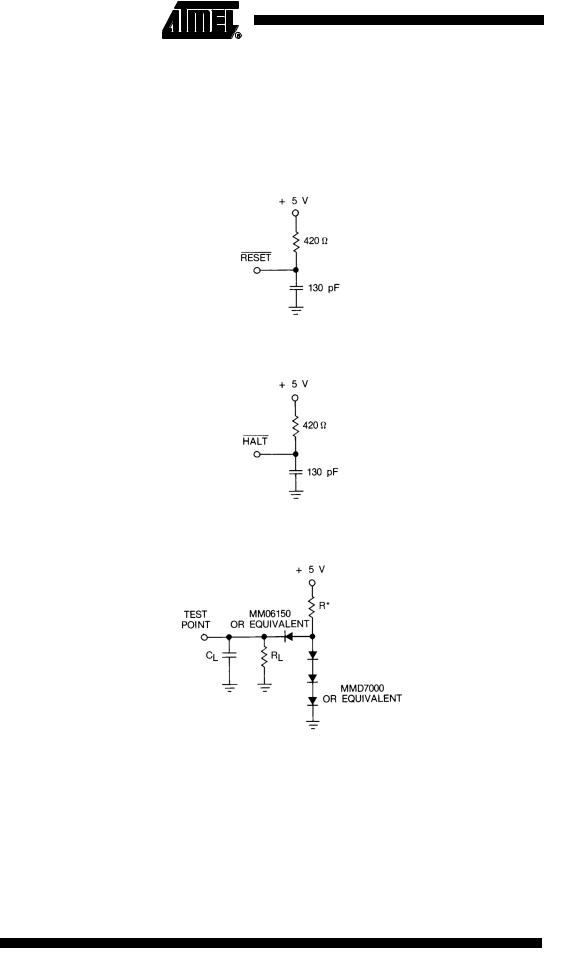
Test Conditions Specific to the Device
Loading Network |
The applicable loading network shall be defined in column “Test conditions” of Table 6, |
|
referring to the loading network number as shown in Figure 6, Figure 7, Figure 8 below. |
|
Figure 6. RESET Test Loads |
Figure 7. HALT Test Load
Figure 8. Test Load
Table 7. Load Network
Load NBR |
Figure |
R |
RL |
CL |
|
Output Application |
|||||||||||||||||
1 |
7 |
2 k |
6.0 k |
50 pF |
|
|
|
|
|
|
|
|
|
|
|
|
|
|
|
|
|
|
|
|
OCS, |
ECS |
|||||||||||||||||||||
|
|
|
|
|
|
|
|
|
|
||||||||||||||
2 |
7 |
1.22 k |
6.0 k |
130 pF |
A0-A31, D0-D31, |
|
|
|
FC0-FC2, SIZ0-SIZ1 |
||||||||||||||
BG, |
|||||||||||||||||||||||
|
|
|
|
|
|
|
|
|
|
|
|
|
|
|
|
|
|||||||
3 |
7 |
0.74 k |
6.0 k |
130 pF |
|
|
|
|
|
|
|
|
|
|
|
|
|
|
|
|
|
|
|
AS, |
DS, |
R/W, |
|
RMC, DBEN, IPEND |
|||||||||||||||||||
|
|
|
|
|
|
|
|
|
|
|
|
|
|
|
|
|
|
|
|
|
|
|
|
Note: 1. Equivalent loading may be simulated by the tester.
14 TS68020
2115A–HIREL–07/02
 Loading...