


ATMEL ATV2500L-35PI, ATV2500L-35PC, ATV2500L-35LI, ATV2500L-35LC, ATV2500L-35KI Datasheet
...Features
•Third Generation Programmable Logic Structure
–Easily Achieves Gate Utilization Factors of 80 Percent
•Increased Logic Flexibility
–86 Inputs and 72 Sum Terms
•Flexible Output Macrocell
–48 Flip-Flops - 2 per Macrocell
–3 Sum Terms - Can Be OR'ed and Shared
•High-Speed
•Low-Power — Less than 0.5 mA Typical (ATV2500L)
•Multiple Feedback Paths Provide for Buried State Machines and I/O Bus Compatibility
•Asynchronous Clocks and Resets
–Multiple Synchronous Presets - One per Four or Eight Flip-Flops
•Proven and Reliable High Speed CMOS EPROM Process
–2000V ESD Protection
–200 mA Latchup Immunity
•Reprogrammable - Tested 100% for Programmability
•40-pin Dual-In-line and 44-Lead Surface Mount Packages
Block Diagram
Description
The ATV2500H/L is the most powerful programmable logic device available in a 40pin package. Increased product terms, sum terms, and flip-flops translate into many more usable gates. High gate utilization is easily obtainable.
The ATV2500H/L is organized around a global bus. All pin and feedback terms are always available to every logic cell. Each of the 38 logic pins and their complements are array inputs, as well as the true and false outputs of each of the 48 flip-flops.
(continued)
Pin Configurations
Pin Name |
Function |
|
|
IN |
Logic Inputs |
|
|
I/O |
Bidirectional Buffers |
|
|
I/O, 0,2,4.. |
“Even” I/O Buffers |
|
|
I/O, 1,3,5.. |
“Odd” I/O Buffers |
|
|
* |
No Internal Connection |
|
|
VCC |
+5V Supply |
|
|
DIP
IN |
|
|
1 |
40 |
|
|
IN |
IN |
|
|
2 |
39 |
|
|
IN |
IN |
|
|
3 |
38 |
|
|
IN |
I/O0 |
|
|
4 |
37 |
|
|
IN |
I/O1 |
|
|
5 |
36 |
|
|
I/O6 |
I/O2 |
|
6 |
35 |
|
|
I/O7 |
|
I/O3 |
|
7 |
34 |
|
|
I/O8 |
|
I/O4 |
|
8 |
33 |
|
|
I/O9 |
|
I/O5 |
|
9 |
32 |
|
|
I/O10 |
|
VCC |
|
10 |
31 |
|
|
I/O11 |
|
I/O17 |
|
11 |
30 |
|
|
GND |
|
I/O16 |
|
12 |
29 |
|
|
I/O23 |
|
I/O15 |
|
13 |
28 |
|
|
I/O22 |
|
I/O14 |
|
14 |
27 |
|
|
I/O21 |
|
I/O13 |
|
15 |
26 |
|
|
I/O20 |
|
I/O12 |
|
16 |
25 |
|
|
I/O19 |
|
IN |
|
17 |
24 |
|
|
I/O18 |
|
IN |
|
18 |
23 |
|
|
IN |
|
IN |
|
19 |
22 |
|
|
IN |
|
IN |
|
20 |
21 |
|
|
IN |
|
|
|
|
|
|
|
|
|
PLCC/LCC
|
I/O1 |
I/O0 |
* |
IN |
IN |
IN |
IN |
IN |
IN |
IN |
I/O06 |
|
I/O2 |
6 |
5 |
4 |
3 |
2 |
1 |
44 |
43 |
42 |
41 |
40 |
I/O7 |
7 |
|
|
|
|
|
|
|
|
|
39 |
||
I/O3 |
8 |
|
|
|
|
|
|
|
|
|
38 |
I/O8 |
I/O4 |
9 |
|
|
|
|
|
|
|
|
|
37 |
I/O9 |
I/O5 |
10 |
|
|
|
|
|
|
|
|
|
36 |
I/O10 |
VCC |
11 |
|
|
|
|
|
|
|
|
|
35 |
I/O11 |
VCC |
12 |
|
|
|
|
|
|
|
|
|
34 |
GND |
I/O17 |
13 |
|
|
|
|
|
|
|
|
|
33 |
GND |
I/O16 |
14 |
|
|
|
|
|
|
|
|
|
32 |
I/O23 |
I/O15 |
15 |
|
|
|
|
|
|
|
|
|
31 |
I/O22 |
I/O14 |
16 |
|
|
|
|
|
|
|
|
|
30 |
I/O21 |
I/O13 |
17 |
19 |
20 |
21 |
22 |
23 |
24 |
25 |
26 |
27 |
29 |
I/O20 |
|
18 |
28 |
|
|||||||||
|
I/O12 |
IN |
IN |
IN |
IN |
IN |
IN |
IN |
* |
I/O18 |
I/O19 |
|
* = No Connect
High-Density |
UV-Erasable |
Programmable |
Logic Device |
ATV2500H |
ATV2500L |
Rev. 0025E–05/98 |
1 |

There are 416 product terms available. Four product terms are input to each sum term. The three sum terms per logic cell can be combined to provide up to twelve product terms, combinatorial and registered. Independent of output configuration, the two flip-flops are always usable, and always have at least four product term inputs.
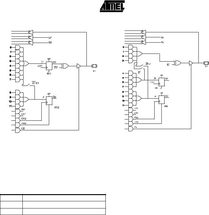
Functional Logic Diagram ATV2500H/L
Product terms are available providing asynchronous resets, flip-flop clocks, and output enables. One reset and one clock term are provided per flip-flop, with one enable term per output. Eight product terms provide local synchronous presets, divided up into banks of four and eight flipflops. Register preload and buried register observability simplify testing. The device has an internal power up clear function.
2 |
ATV2500H/L |
|
|
||
|

Functional Logic Diagram Description
The ATV2500H/L Functional Logic Diagram describes the interconnections between the input, feedback pins and logic cells. All interconnections are routed through the global bus.
The ATV2500H/L is a straightforward and uniform PLD. The twenty-four macrocells are numbered 0 through 23. Each macrocell contains 17 AND gates. All AND gates have 172 inputs. The five lower product terms provide AR1, CK1, CK2, AR2, and OE. These are: one asynchronous reset and clock per flip-flop, and an output enable. The top
Absolute Maximum Ratings*
...............................Temperature Under Bias |
-55°C to + 125°C |
|
Storage Temperature .................................... |
-65°C to + 150°C |
|
Voltage on Any Pin with |
-2.0V to +7.0V(1) |
|
Respect to Ground ......................................... |
||
Voltage on Input Pins |
|
|
with Respect to Ground |
-2.0V to +14.0V(1) |
|
During Programming..................................... |
||
Programming Voltage with |
-2.0V to +14.0V(1) |
|
Respect to Ground ....................................... |
||
Integrated UV Erase Dose.............................. |
7258 W.sec/cm2 |
|
|
|
|
|
|
|
|
|
|
ATV2500H/L
twelve product terms are grouped into three sum terms, which are used as shown in the macrocell diagrams.
Eight synchronous preset terms are distributed in a 2/4 pattern. The first four macrocells share Preset 0, the next two share Preset 1, and so on, ending with the last two macrocells sharing Preset 7.
The fourteen dedicated inputs and their complements use the numbered positions in the global bus as shown. Each macrocell provides six inputs to the global bus: (left to right) flip-flop Q2 true and false, flip-flop Q1 true and false, and the pin true and false. The positions occupied by these signals in the global bus are the six numbers in the bus diagram next to each macrocell.
*NOTICE: Stresses beyond those listed under “Absolute Maximum Ratings” may cause permanent damage to the device. This is a stress rating only and functional operation of the device at these or any other conditions beyond those indicated in the operational sections of this specification is not implied. Exposure to absolute maximum rating conditions for extended periods may affect device reliability.
Note: 1. Minimum voltage is -0.6V dc, which may undershoot to -2.0V for pulses of less than 20 ns. Maximum output pin voltage is Vcc + 0.75V dc, which may overshoot to 7.0V for pulses of less than 20 ns.
3
|
|
|
|
|
|
|
|
|
|
|
|
|
|
|
|
|
|
Output Logic, Registered |
Output Logic, Combinatorial |
||||
These diagrams show equivalent logic functions, not necessarily the actual circuit implementation.
|
|
|
|
Terms In |
|
|
|
|
|
|
|
|
|
S2 |
S1 |
|
S0 |
D1 |
D2 |
Output Configuration |
|
|
|
|
|
|
|
0 |
0 |
|
0 |
8 |
4 |
Registered (Q1) |
|
|
|
|
|
|
|
0 |
1 |
|
0 |
12 |
4(1) |
Registered (Q1) |
Note: |
1. |
These 4 terms are shared with D1. |
||||
S3 Output Configuration
0Active Low
1Active High
|
|
|
|
Terms In |
|
|
|
|
|
|
|
|
|
S2 |
S1 |
|
S0 |
D1 |
D2 |
Output Configuration |
|
|
|
|
|
|
|
1 |
0 |
|
0 |
4(1) |
4 |
Combinatorial (8 Terms) |
1 |
0 |
|
1 |
4 |
4 |
Combinatorial (4 Terms) |
|
|
|
|
|
|
|
1 |
1 |
|
0 |
4(1) |
4(1) |
Combinatorial (12 Terms) |
Note: |
1. |
These 4 terms are shared with D1. |
||||
S3 |
Output Configuration |
|
|
0 |
Active Low |
|
|
1 |
Active High |
|
|
DC and AC Operating
|
|
ATV2500H-25 |
ATV2500H/L-30 |
ATV2500H/L-35 |
|
|
|
|
|
|
|
Operating |
Com. |
0°C - 70°C |
0°C - 70°C |
0°C - 70°C |
|
Temperature |
|
|
|
|
|
Ind. |
-40°C - 85°C |
-40°C - 85°C |
-40°C - 85°C |
||
(Case) |
|||||
|
|
|
|
||
|
Mil. |
-55°C - 125°C |
-55°C - 125°C |
-55°C - 125°C |
|
|
|
|
|
|
|
VCC Power Supply |
|
5V ± 10% |
5V ± 10% |
5V ± 10% |
|
|
|
|
|
|
4 |
ATV2500H/L |
|
|
||
|

ATV2500H/L
DC Characteristics
Symbol |
Parameter |
Condition |
|
|
Min |
Typ |
Max |
Units |
|
|
|
|
|
|
|
|
|
ILI |
Input Load Current |
VIN = -0.1V to VCC + 1V |
|
|
|
10 |
μA |
|
ILO |
Output Leakage |
VOUT = -0.1V to VCC + 0.1V |
|
|
|
10 |
μA |
|
|
Current |
|
|
|
|
|
|
|
|
|
|
|
|
|
|
|
|
ICC |
Power Supply |
VCC = MAX, |
ATV2500L |
Com. |
|
0.5 |
5 |
mA |
|
Current |
VIN = GND or VCC |
|
|
|
|
|
|
|
|
Ind.,Mil. |
|
0.5 |
10 |
mA |
||
|
|
Outputs Open |
|
|
||||
|
|
|
|
|
|
|
|
|
|
|
|
ATV2500H |
Com. |
|
80 |
160 |
mA |
|
|
|
|
|
|
|
|
|
|
|
|
|
Ind.,Mil. |
|
80 |
180 |
mA |
|
|
|
|
|
|
|
|
|
(1) |
Output Short |
VOUT = 0.5V |
|
|
|
|
-120 |
mA |
IOS |
|
|
|
|
||||
|
Circuit Current |
|
|
|
|
|
|
|
|
|
|
|
|
|
|
|
|
VIL |
Input Low Voltage |
|
|
|
-0.6 |
|
0.8 |
V |
VIH |
Input High Voltage |
|
|
|
2.0 |
|
VCC + 0.75 |
V |
VOL |
Output Low Voltage |
VIN = VIH or VIL, |
|
|
|
|
0.5 |
V |
|
|
IOL = 8 mA Com,Ind; 6 mA Mil. |
|
|
|
|
|
|
VOH |
Output High Voltage |
IOH = -100 μA |
|
|
VCC - 0.3 |
|
|
V |
|
|
IOH = -4.0 mA |
|
|
2.4 |
|
|
V |
Note: |
1. |
Not more than one output at a time should be shorted. Duration of short circuit test should not exceed 30 sec. This parame- |
||||
|
|
ter is only sampled and is not 100% tested. See Absolute Maximum Ratings. |
|
|||
Pin Capacitance (f = MHz, T = 25°C)(1) |
|
|
||||
|
|
|
Typ |
Max |
Units |
Conditions |
|
|
|
|
|
|
|
CIN |
|
|
4 |
6 |
pF |
VIN = OV |
COUT |
|
|
8 |
12 |
pF |
VOUT = OV |
Note: |
1. |
Typical values for nominal supply voltage. This parameter is only sampled and is not 100% tested. |
||||
5
 Loading...