


 Loading...
ATMEL ATmega163L-4PI, ATmega163L-4PC, ATmega163L-4AI, ATmega163L-4AC, ATmega163-8PI Datasheet
...Features
•High-performance, Low-power AVR® 8-bit Microcontroller
–130 Powerful Instructions – Most Single Clock Cycle Execution
–32 x 8 General Purpose Working Registers
–Fully Static Operation
–Up to 8 MIPS Throughput at 8 MHz
–On-chip 2-cycle Multiplier
•Nonvolatile Program and Data Memories
•Self-programming In-System Programmable Flash Memory
–16K Bytes with Optional Boot Block (256 - 2K Bytes) Endurance: 1,000 Write/Erase Cycles
–Boot Section Allows Reprogramming of Program Code without External Programmer
–Optional Boot Code Section with Independent Lock Bits
–512 Bytes EEPROM
Endurance: 100,000 Write/Erase Cycles
–1024 Bytes Internal SRAM
–Programming Lock for Software Security
•Peripheral Features
–Two 8-bit Timer/Counters with Separate Prescaler and Compare Mode
–One 16-bit Timer/Counter with Separate Prescaler, Compare Mode, and Capture Mode
–Real Time Clock with Separate Oscillator and Counter Mode
–Three PWM Channels
–8-channel, 10-bit ADC
–Byte-oriented Two-wire Serial Interface
–Programmable Serial UART
–Master/Slave SPI Serial Interface
–Programmable Watchdog Timer with Separate On-chip Oscillator
–Analog Comparator
•Special Microcontroller Features
–Power-on Reset and Programmable Brown-out Detection
–Internal Calibrated RC Oscillator
–External and Internal Interrupt Sources
–Four Sleep Modes: Idle, ADC Noise Reduction, Power-save, and Power-down
•Power Consumption at 4 MHz, 3.0V, 25°C
–Active 5.0 mA
–Idle Mode 1.9 mA
–Power-down Mode < 1 µA
•I/O and Packages
–32 Programmable I/O Lines
–40-pin PDIP and 44-pin TQFP
•Operating Voltages
–2.7 - 5.5V for ATmega163L
–4.0 - 5.5V for ATmega163
•Speed Grades
–0 - 4 MHz for ATmega163L
–0 - 8 MHz for ATmega163
8-bit |
Microcontroller |
with 16K Bytes |
In-System |
Programmable |
Flash |
ATmega163 |
ATmega163L |
Not Recommend for |
New Designs. Use |
ATmega16. |
Rev. 1142E–AVR–02/03 |
1 |
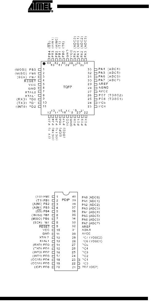
Pin Configurations
(SCL) |
(SDA) |
|
|
|
|
|
|
|
|
|
|
|
|
|
|
|
|
|
|
|
|
|
|
|
|
|
|
|
|
|
|
|
|
|
|
|
|
|
|
|
|
|
|
|
|
|
|
|
|
|
|
|
|
|
|
|
|
|
|
|
|
|
|
|
|
|
|
|
|
(SDA)
(SCL)
2 ATmega163(L)
1142E–AVR–02/03

 ATmega163(L)
Description
Block Diagram
The ATmega163 is a low-power CMOS 8-bit microcontroller based on the AVR architecture. By executing powerful instructions in a single clock cycle, the ATmega163 achieves throughputs approaching 1 MIPS per MHz allowing the system designer to optimize power consumption versus processing speed.
Figure 1. |
Block Diagram |
|
|
|
|
|
PA0 - PA7 |
PC0 - PC7 |
|
||
VCC |
|
|
|
|
|
|
PORTA DRIVERS |
PORTC DRIVERS |
|
||
GND |
|
|
|
|
|
|
DATA REGISTER |
DATA DIR. |
DATA REGISTER |
DATA DIR. |
|
|
PORTA |
REG. PORTA |
PORTC |
REG. PORTC |
|
|
|
8-BIT DATA BUS |
|
|
|
AVCC |
|
|
|
|
|
|
ANALOG MUX |
ADC |
|
|
|
AGND |
|
|
2-WIRE SERIAL |
OSCILLATOR |
|
|
|
|
XTAL1 |
||
AREF |
|
|
INTERFACE |
|
|
|
|
|
|
||
|
INTERNAL |
|
INTERNAL |
|
|
|
REFERENCE |
|
OSCILLATOR |
|
|
|
|
OSCILLATOR |
|
||
|
|
|
|
|
|
|
PROGRAM |
STACK |
WATCHDOG |
TIMING AND |
XTAL2 |
|
RESET |
||||
|
COUNTER |
POINTER |
TIMER |
CONTROL |
|
|
|
||||
|
PROGRAM |
SRAM |
MCU CONTROL |
|
|
|
FLASH |
REGISTER |
|
|
|
|
|
|
|
||
|
INSTRUCTION |
GENERAL |
TIMER/ |
|
|
|
REGISTER |
PURPOSE |
COUNTERS |
|
|
|
REGISTERS |
|
|
|
|
|
INSTRUCTION |
X |
INTERRUPT |
|
|
|
Y |
|
|
||
|
UNIT |
|
|
||
|
DECODER |
Z |
|
|
|
|
|
|
|
||
|
CONTROL |
ALU |
EEPROM |
|
|
|
LINES |
|
|
||
|
|
|
|
|
|
|
|
|
INTERNAL |
|
|
|
|
STATUS |
CALIBRATED |
|
|
|
|
REGISTER |
OSCILLATOR |
|
|
|
PROGRAMMING |
SPI |
UART |
|
|
|
LOGIC |
|
|
||
|
|
|
|
|
|
+ - |
ANALOG COMPARATOR |
DATA REGISTER |
|
|
|
DATA DIR. |
||||||||||||||
|
|
|
PORTB |
|
|
REG. PORTB |
||||||||||||
|
|
|
|
|
|
|
|
|
|
|
|
|
|
|
|
|
|
|
PORTB DRIVERS
PB0 - PB7
|
|
|
|
|
|
|
|
|
|
|
|
|
|
|
|
|
|
|
|
|
|
|
|
|
|
|
|
|
|
|
|
|
|
|
|
|
|
|
|
|
|
|
|
|
|
|
|
|
|
|
|
|
|
|
|
|
DATA REGISTER |
|
|
|
DATA DIR. |
||||||||||||||
|
|
|
PORTD |
|
|
REG. PORTD |
||||||||||||
|
|
|
|
|
|
|
|
|
|
|
|
|
|
|
|
|
|
|
PORTD DRIVERS
PD0 - PD7
The AVR core combines a rich instruction set with 32 general purpose working registers. All the 32 registers are directly connected to the Arithmetic Logic Unit (ALU), allowing two independent registers to be accessed in one single instruction executed in one clock
3
1142E–AVR–02/03

|
|
|
|
|
|
|
|
|
|
|
|
|
cycle. The resulting architecture is more code efficient while achieving throughputs up to |
||||
|
ten times faster than conventional CISC microcontrollers. |
||||
|
The ATmega163 provides the following features: 16K bytes of In-System Self-Program- |
||||
|
mable Flash, 512 bytes EEPROM, 1024 bytes SRAM, 32 general purpose I/O lines, 32 |
||||
|
general purpose working registers, three flexible Timer/Counters with compare modes, |
||||
|
internal and external interrupts, a byte oriented Two-wire Serial Interface, an 8-channel, |
||||
|
10-bit ADC, a programmable Watchdog Timer with internal Oscillator, a programmable |
||||
|
serial UART, an SPI serial port, and four software selectable power saving modes. The |
||||
|
Idle mode stops the CPU while allowing the SRAM, Timer/Counters, SPI port, and inter- |
||||
|
rupt system to continue functioning. The Power-down mode saves the register contents |
||||
|
but freezes the Oscillator, disabling all other chip functions until the next interrupt or |
||||
|
Hardware Reset. In Power-save mode, the asynchronous Timer Oscillator continues to |
||||
|
run, allowing the user to maintain a timer base while the rest of the device is sleeping. |
||||
|
The ADC Noise Reduction mode stops the CPU and all I/O modules except asynchro- |
||||
|
nous timer and ADC, to minimize switching noise during ADC conversions. |
||||
|
The On-chip ISP Flash can be programmed through an SPI serial interface or a conven- |
||||
|
tional programmer. By installing a Self-Programming Boot Loader, the microcontroller |
||||
|
can be updated within the application without any external components. The Boot Pro- |
||||
|
gram can use any interface to download the application program in the Application Flash |
||||
|
memory. By combining an 8-bit CPU with In-System Self-Programmable Flash on a |
||||
|
monolithic chip, the Atmel ATmega163 is a powerful microcontroller that provides a |
||||
|
highly flexible and cost effective solution to many embedded control applications. |
||||
|
The ATmega163 AVR is supported with a full suite of program and system development |
||||
|
tools including: C compilers, macro assemblers, program debugger/simulators, In-Cir- |
||||
|
cuit Emulators, and evaluation kits. |
||||
Pin Descriptions |
|
|
|
|
|
VCC |
Digital supply voltage. |
||||
GND |
Digital ground. |
||||
Port A (PA7..PA0) |
Port A serves as the analog inputs to the A/D Converter. |
||||
|
Port A also serves as an 8-bit bi-directional I/O port, if the A/D Converter is not used. |
||||
|
Port pins can provide internal pull-up resistors (selected for each bit). The Port A output |
||||
|
buffers can sink 20mA and can drive LED displays directly. When pins PA0 to PA7 are |
||||
|
used as inputs and are externally pulled low, they will source current if the internal pull- |
||||
|
up resistors are activated. The Port A pins are tristated when a reset condition becomes |
||||
|
active, even if the clock is not running. |
||||
Port B (PB7..PB0) |
Port B is an 8-bit bi-directional I/O port with internal pull-up resistors (selected for each |
||||
|
bit). The Port B output buffers can sink 20 mA. As inputs, Port B pins that are externally |
||||
|
pulled low will source current if the pull-up resistors are activated. Port B also serves the |
||||
|
functions of various special features of the ATmega83/163 as listed on page 117. The |
||||
|
Port B pins are tristated when a reset condition becomes active, even if the clock is not |
||||
|
running. |
||||
Port C (PC7..PC0) |
Port C is an 8-bit bi-directional I/O port with internal pull-up resistors (selected for each |
||||
|
bit). The Port C output buffers can sink 20 mA. As inputs, Port C pins that are externally |
||||
|
pulled low will source current if the pull-up resistors are activated. The Port C pins are |
||||
|
tristated when a reset condition becomes active, even if the clock is not running. |
||||
4 ATmega163(L)
1142E–AVR–02/03

|
|
|
|
ATmega163(L) |
||
|
|
|
|
|||
|
|
|
|
|||
|
|
|
Port C also serves the functions of various special features of the ATmega163 as listed |
|||
|
|
|
||||
|
|
|
on page 124. |
|
|
|
|
Port D (PD7..PD0) |
Port D is an 8-bit bidirectional I/O port with internal pull-up resistors (selected for each |
||||
|
|
|
bit). The Port D output buffers can sink 20 mA. As inputs, Port D pins that are externally |
|||
|
|
|
pulled low will source current if the pull-up resistors are activated. Port D also serves the |
|||
|
|
|
functions of various special features of the ATmega163 as listed on page 128. The Port |
|||
|
|
|
D pins are tristated when a reset condition becomes active, even if the clock is not |
|||
|
|
|
running. |
|
|
|
|
|
|
|
|
|
|
|
RESET |
Reset input. A low level on this pin for more than 500 ns will generate a Reset, even if |
||||
|
|
|
the clock is not running. Shorter pulses are not guaranteed to generate a Reset. |
|||
|
XTAL1 |
Input to the inverting Oscillator amplifier and input to the internal clock operating circuit. |
||||
|
XTAL2 |
Output from the inverting Oscillator amplifier. |
|
|
||
|
AVCC |
This is the supply voltage pin for Port A and the A/D Converter. It should be externally |
||||
|
|
|
connected to VCC, even if the ADC is not used. If the ADC is used, it should be con- |
|||
|
|
|
nected to VCC through a low-pass filter. See page 105 for details on operation of the |
|||
|
|
|
ADC. |
|
|
|
|
AREF |
AREF is the analog reference input pin for the A/D Converter. For ADC operations, a |
||||
|
|
|
voltage in the range 2.5V to AVCC can be applied to this pin. |
|
|
|
|
AGND |
Analog ground. If the board has a separate analog ground plane, this pin should be con- |
||||
|
|
|
nected to this ground plane. Otherwise, connect to GND. |
|
|
|
|
Clock Options |
The device has the following clock source options, selectable by Flash Fuse bits as |
||||
|
|
|
shown: |
|
|
|
|
|
|
Table 1. Device Clocking Options Select(1) |
|
|
|
|
|
|
Device Clocking Option |
CKSEL3..0 |
|
|
|
|
|
|
|
|
|
|
|
|
External Crystal/Ceramic Resonator |
1111 - 1010 |
|
|
|
|
|
|
|
|
|
|
|
|
External Low-frequency Crystal |
1001 - 1000 |
|
|
|
|
|
|
|
|
|
|
|
|
External RC Oscillator |
0111 - 0101 |
|
|
|
|
|
|
|
|
|
|
|
|
Internal RC Oscillator |
0100 - 0010 |
|
|
|
|
|
|
|
|
|
|
|
|
External Clock |
0001 - 0000 |
|
|
|
|
|
|
|
|
|
|
|
|
Note: 1. “1” means unprogrammed, “0” means programmed. |
|
|
|
|
|
|
The various choices for each clocking option give different start-up times as shown in |
|||
|
|
|
Table 5 on page 25. |
|
|
|
|
Internal RC Oscillator |
The internal RC Oscillator option is an On-chip Oscillator running at a fixed frequency of |
||||
|
|
|
nominally 1 MHz. If selected, the device can operate with no external components. The |
|||
|
|
|
device is shipped with this option selected. See “EEPROM Read/Write Access” on page |
|||
|
|
|
62 for information on calibrating this Oscillator. |
|
|
|
5
1142E–AVR–02/03

Crystal Oscillator |
|
|
|
|
|
|
|
|
|
|
|
|
|
|
|
|
|
|
|
|
|
|
|
|
|
XTAL1 and XTAL2 are input and output, respectively, of an inverting amplifier which can |
||||||||||||
|
be configured for use as an On-chip Oscillator, as shown in Figure 2. Either a quartz |
|||||||||||
|
crystal or a ceramic resonator may be used. |
|||||||||||
|
Figure 2. Oscillator Connections |
|||||||||||
|
|
|
|
|
|
|
|
|
|
|
|
|
|
|
|
|
|
|
|
|
|
|
|
|
|
|
|
|
|
|
|
|
|
|
|
|
|
|
|
|
|
|
|
|
|
|
|
|
|
|
|
|
|
|
|
|
|
|
|
|
|
|
|
|
|
|
|
|
|
|
|
|
|
|
|
|
|
|
|
|
|
|
|
|
|
|
|
|
|
|
|
|
|
|
|
|
|
|
|
|
|
|
|
|
|
|
|
|
|
|
|
|
|
|
|
|
External Clock |
To drive the device from an external clock source, XTAL1 should be driven as shown in |
||||||||||
|
Figure 3. |
||||||||||
|
Figure 3. External Clock Drive Configuration |
||||||||||
|
|
|
|
|
|
|
|
|
|
|
|
|
|
|
|
|
|
|
|
|
|
|
|
|
|
|
|
|
|
|
|
|
|
|
|
|
|
|
|
|
|
|
|
|
|
|
|
|
|
|
|
|
|
|
|
|
|
|
|
|
|
|
|
|
|
|
|
|
|
|
|
|
|
|
|
|
|
|
|
|
|
|
|
|
|
|
|
|
|
|
|
|
|
|
|
External RC Oscillator |
For timing insensitive applications, the external RC configuration shown in Figure 4 can |
|
be used. For details on how to choose R and C, see Table 64 on page 162. |
|
Figure 4. External RC Configuration |
Timer Oscillator
|
VCC |
|
R |
NC |
XTAL2 |
|
|
|
|
|
XTAL1 |
C |
|
GND |
|
|
For the Timer Oscillator pins, TOSC1 and TOSC2, the crystal is connected directly between the pins. No external capacitors are needed. The Oscillator is optimized for use with a 32,768 Hz watch crystal. Applying an external clock source to the TOSC1 pin is not recommended.
6 ATmega163(L)
1142E–AVR–02/03

Architectural
Overview
1142E–AVR–02/03
ATmega163(L)
The fast-access Register File concept contains 32 x 8-bit general purpose working registers with a single clock cycle access time. This means that during one single clock cycle, one Arithmetic Logic Unit (ALU) operation is executed. Two operands are output from the Register File, the operation is executed, and the result is stored back in the Register File – in one clock cycle.
Six of the 32 registers can be used as three 16-bits indirect address register pointers for Data Space addressing – enabling efficient address calculations. One of the three address pointers is also used as the address pointer for look-up tables in Flash Program memory. These added function registers are the 16-bits X-, Y-, and Z-register.
The ALU supports arithmetic and logic operations between registers or between a constant and a register. Single register operations are also executed in the ALU. Figure 5 shows the ATmega163 AVR Enhanced RISC microcontroller architecture.
In addition to the register operation, the conventional Memory Addressing modes can be used on the Register File as well. This is enabled by the fact that the Register File is assigned the 32 lowest Data Space addresses ($00 - $1F), allowing them to be accessed as though they were ordinary memory locations.
The I/O Memory space contains 64 addresses for CPU peripheral functions as Control Registers, Timer/Counters, A/D-converters, and other I/O functions. The I/O Memory can be accessed directly, or as the Data Space locations following those of the Register File, $20 - $5F.
7
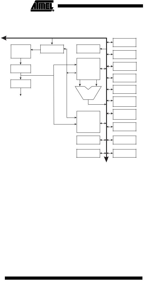
Figure 5. The ATmega163 AVR RISC Architecture
Data Bus 8-bit
|
|
|
|
Interrupt |
|
Program |
|
Status |
Unit |
8K X 16 |
|
|
||
Counter |
|
and Control |
|
|
Program |
|
SPI |
||
|
|
|
||
Memory |
|
|
|
Unit |
|
|
|
32 x 8 |
Serial |
Instruction |
|
|
General |
|
|
|
UART |
||
Register |
|
|
Purpose |
|
|
|
|
||
|
|
|
Registrers |
Two-wire Serial |
|
|
|
|
|
Instruction |
|
|
|
Interface |
|
|
|
|
|
Decoder |
|
IndirectAddressing |
|
8-bit |
|
DirectAddressing |
|
||
|
ALU |
Timer/Counter |
||
|
|
|||
Control Lines |
|
16-bit |
||
|
|
Timer/Counter |
||
|
|
with PWM |
||
|
|
8-bit |
||
|
|
|
|
|
|
|
|
|
Timer/Counter |
|
|
|
1024 x 8 |
with PWM |
|
|
|
|
|
|
|
|
Data |
Watchdog |
|
|
|
SRAM |
|
|
|
|
|
Timer |
|
|
|
512 x 8 |
A/D Converter |
|
|
|
EEPROM |
|
|
|
|
|
|
|
|
|
32 |
Analog |
|
|
|
I/O Lines |
Comparator |
The AVR uses a Harvard architecture concept – with separate memories and buses for program and data. The Program memory is executed with a two stage pipeline. While one instruction is being executed, the next instruction is pre-fetched from the Program memory. This concept enables instructions to be executed in every clock cycle. The Program memory is In-System Re-programmable Flash memory.
With the jump and call instructions, the whole 8K word address space is directly accessed. Most AVR instructions have a single 16-bit word format. Every program memory address contains a 16or 32-bit instruction.
Program Flash memory space is divided in two sections, the Boot Program section (256 to 2,048 bytes, see page 134) and the Application Program section. Both sections have dedicated Lock bits for write and read/write protection. The SPM instruction that writes into the Application Flash memory section is allowed only in the Boot Program section.
During interrupts and subroutine calls, the return address Program Counter (PC) is stored on the Stack. The Stack is effectively allocated in the general data SRAM, and consequently the Stack size is only limited by the total SRAM size and the usage of the SRAM. All user programs must initialize the SP in the reset routine (before subroutines or interrupts are executed). The 11-bit Stack Pointer SP is read/write accessible in the I/O space.
8 ATmega163(L)
1142E–AVR–02/03
 ATmega163(L)
The 1,024 bytes data SRAM can be easily accessed through the five different addressing modes supported in the AVR architecture.
The memory spaces in the AVR architecture are all linear and regular memory maps.
A flexible interrupt module has its Control Registers in the I/O space with an additional Global Interrupt Enable bit in the Status Register. All interrupts have a separate Interrupt Vector in the Interrupt Vector table at the beginning of the Program memory. The interrupts have priority in accordance with their Interrupt Vector position. The lower the Interrupt Vector address, the higher the priority.
Figure 6. Memory Maps
Program Memory
$0000
Application Flash Section
Boot Flash Section
$1FFF
9
1142E–AVR–02/03

The General Purpose
Register File
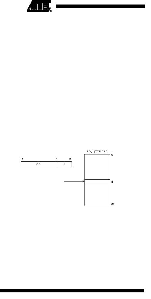
Figure 7 shows the structure of the 32 general purpose working registers in the CPU.
Figure 7. AVR CPU General Purpose Working Registers
7 |
0 |
Addr. |
|
|
|
|
R0 |
$00 |
|
|
|
|
|
|
|
|
R1 |
$01 |
|
|
|
|
|
|
|
|
R2 |
$02 |
|
|
|
|
|
|
|
|
… |
|
|
|
|
|
|
|
|
|
R13 |
$0D |
|
|
|
|
|
|
General |
|
R14 |
$0E |
|
|
|
|
|
|
Purpose |
|
R15 |
$0F |
|
|
|
|
|
|
Working |
|
R16 |
$10 |
|
|
|
|
|
|
Registers |
|
R17 |
$11 |
|
|
|
|
|
|
|
|
… |
|
|
|
|
|
|
|
|
|
R26 |
$1A |
X-register Low Byte |
|
|
|
|
|
|
|
R27 |
$1B |
X-register High Byte |
|
|
|
|
|
|
|
R28 |
$1C |
Y-register Low Byte |
|
|
|
|
|
|
|
R29 |
$1D |
Y-register High Byte |
|
|
|
|
|
|
|
R30 |
$1E |
Z-register Low Byte |
|
|
|
|
|
|
|
R31 |
$1F |
Z-register High Byte |
|
|
|
|
|
All the register operating instructions in the instruction set have direct and single cycle access to all registers. The only exception is the five constant arithmetic and logic instructions SBCI, SUBI, CPI, ANDI, and ORI between a constant and a register, and the LDI instruction for load immediate constant data. These instructions apply to the second half of the registers in the Register File – R16..R31. The general SBC, SUB, CP, AND, and OR and all other operations between two registers or on a single register apply to the entire Register File.
As shown in Figure 7, each register is also assigned a data memory address, mapping them directly into the first 32 locations of the user Data Space. Although not being physically implemented as SRAM locations, this memory organization provides great flexibility in access of the registers, as the X-, Y-, and Z-registers can be set to index any register in the file.
The X-register, Y-register, and The registers R26..R31 have some added functions to their general purpose usage. Z-register These registers are address pointers for indirect addressing of the Data Space. The
three indirect address registers X, Y, and Z are defined as:
Figure 8. The X-, Y-, and Z-registers
|
15 |
XH |
|
XL |
0 |
X - register |
7 |
|
0 |
7 |
0 |
|
|
|
|
|
|
|
R27 ($1B) |
|
|
R26 ($1A) |
|
|
15 |
YH |
|
YL |
0 |
|
|
|
|
|
|
Y - register |
7 |
|
0 |
7 |
0 |
|
|
|
|
|
|
|
R29 ($1D) |
|
|
R28 ($1C) |
|
|
15 |
ZH |
|
ZL |
0 |
|
|
|
|
|
|
Z - register |
7 |
|
0 |
7 |
0 |
|
|
|
|
|
|
|
R31 ($1F) |
|
|
R30 ($1E) |
|
10 ATmega163(L)
1142E–AVR–02/03
 ATmega163(L)
The ALU – Arithmetic
Logic Unit
In the different addressing modes these address registers have functions as fixed displacement, automatic increment and decrement (see the descriptions for the different instructions).
The high-performance AVR ALU operates in direct connection with all the 32 general purpose working registers. Within a single clock cycle, ALU operations between registers in the Register File are executed. The ALU operations are divided into three main categories – arithmetic, logical, and bit-functions. ATmega163 also provides a powerful multiplier supporting both signed/unsigned multiplication and fractional format. See the Instruction Set section for a detailed description.
The In-System Self-
Programmable Flash
Program Memory
The SRAM Data Memory
1142E–AVR–02/03
The ATmega163 contains 16K bytes On-chip In-System Self-Programmable Flash memory for program storage. Since all instructions are 16or 32-bit words, the Flash is organized as 8K x 16. The Flash Program memory space is divided in two sections, Boot Program section and Application Program section.
The Flash memory has an endurance of at least 1,000 write/erase cycles. The ATmega163 Program Counter (PC) is 13 bits wide, thus addressing the 8,192 Program Memory locations. The operation of Boot Program section and associated Boot Lock bits for software protection are described in detail on page 134. See also page 154 for a detailed description on Flash data serial downloading.
Constant tables can be allocated within the entire Program Memory address space (see the LPM – Load Program Memory instruction description).
See also page 12 for the different Program Memory Addressing modes.
Figure 9 shows how the ATmega163 SRAM Memory is organized.
Figure 9. SRAM Organization
Register File
R0
R1
R2
...
R29
R30
R31
I/O Registers
$00
$01
$02
...
$3D
$3E
$3F
Data Address Space
$0000
$0001
$0002
...
$001D
$001E
$001F
$0020
$0021
$0022
...
$005D
$005E
$005F
Internal SRAM
$0060
$0061
...
$045E
$045F
11
The Program and Data
Addressing Modes
Register Direct, Single
Register Rd
The lower 1,120 Data Memory locations address the Register File, the I/O Memory, and the internal data SRAM. The first 96 locations address the Register File + I/O Memory, and the next 1,024 locations address the internal data SRAM.
The five different addressing modes for the data memory cover: Direct, Indirect with Displacement, Indirect, Indirect with Pre-decrement, and Indirect with Post-increment. In the Register File, registers R26 to R31 feature the indirect Addressing Pointer Registers.
The direct addressing reaches the entire data space.
The Indirect with Displacement mode features a 63 address locations reach from the base address given by the Y- or Z-register.
When using register indirect addressing modes with automatic pre-decrement and postincrement, the address registers X, Y, and Z are decremented and incremented.
The 32 general purpose working registers, 64 I/O Registers, and the 1,024 bytes of internal data SRAM in the ATmega163 are all accessible through all these addressing modes.
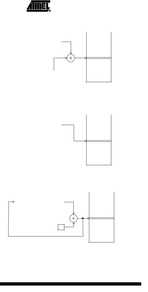
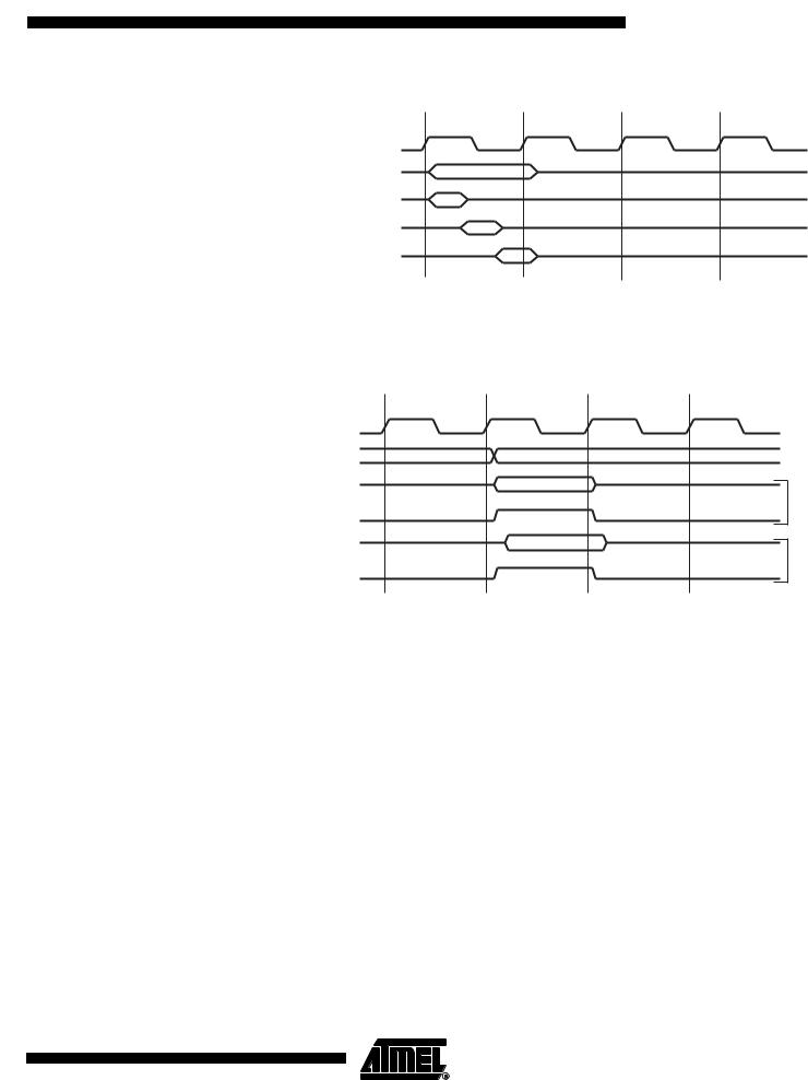
The ATmega163 AVR Enhanced RISC microcontroller supports powerful and efficient addressing modes for access to the Program Memory (Flash) and Data Memory (SRAM, Register File, and I/O Memory). This section describes the different addressing modes supported by the AVR architecture. In the figures, OP means the operation code part of the instruction word. To simplify, not all figures show the exact location of the addressing bits.
Figure 10. Direct Single Register Addressing
The operand is contained in register d (Rd).
12 ATmega163(L)
1142E–AVR–02/03

ATmega163(L)
Register Direct, Two Registers Figure 11. Direct Register Addressing, Two Registers
Rd And Rr
|
Operands are contained in register r (Rr) and d (Rd). The result is stored in register d |
|
(Rd). |
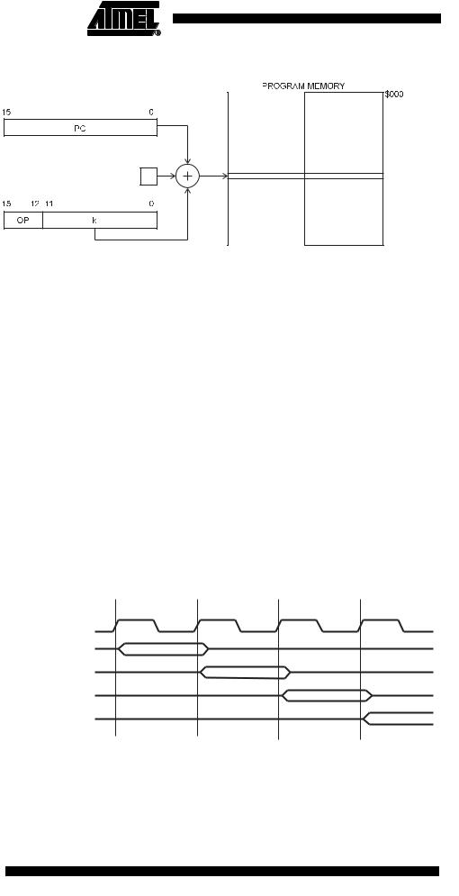
I/O Direct |
Figure 12. I/O Direct Addressing |
Operand address is contained in 6 bits of the instruction word. n is the destination or source register address.
Data Direct |
Figure 13. Direct Data Addressing |
|
|
|
|
|||
|
|
|
|
|
|
|
Data Space |
|
|
31 |
20 19 |
16 |
|
||||
|
|
|
$0000 |
|||||
|
|
OP |
|
Rr/Rd |
|
|
|
|
|
|
|
|
|
|
|
|
|
|
|
16 LSBs |
|
|
|
|
|
|
|
|
|
|
|
|
|
|
|
|
15 |
|
|
0 |
|
|
|
|
$045F
A 16-bit Data Address is contained in the 16 LSBs of a two-word instruction. Rd/Rr specify the destination or source register.
13
1142E–AVR–02/03
|
|
|
|
|
|
|
|
|
|
|
|
|
|
|
|
|
|
|
|
|
|
Data Indirect with |
Figure 14. Data Indirect with Displacement |
|||||||||
Displacement |
|
|
|
|
|
|
|
|
Data Space |
|
|
|
|
|
|
|
|
|
|
||
|
15 |
0 |
|
|
$0000 |
|||||
|
|
|||||||||
|
|
|
|
|||||||
|
|
|
|
|
||||||
|
|
|
Y OR Z - REGISTER |
|
|
|
||||
|
|
|
|
|
|
|
|
|
|
|
15 |
10 |
6 |
5 |
0 |
|
|
OP |
n |
|
|
a |
|
|
|
|
|
|
$045F
Operand address is the result of the Y- or Z-register contents added to the address contained in 6 bits of the instruction word.
Data Indirect |
Figure 15. Data Indirect Addressing |
|
|
|
|
|
|
|
|
|
|
Data Space |
|
|
15 |
0 |
|
|
$0000 |
|
|
|
|||||
|
|
|
|
|||
|
|
X, Y OR Z - REGISTER |
|
|
|
|
$045F
|
Operand address is the contents of the X-, Y-, or the Z-register. |
|||||
Data Indirect with Pre- |
Figure 16. Data Indirect Addressing with Pre-decrement |
|||||
decrement |
|
|
|
|
Data Space |
|
|
|
|
|
|
||
|
15 |
0 |
|
|
$0000 |
|
|
|
|||||
|
|
|
|
|||
|
|
|
X, Y OR Z - REGISTER |
|
|
|
-1
$045F
The X-, Y-, or the Z-register is decremented before the operation. Operand address is the decremented contents of the X-, Y-, or the Z-register.
14 ATmega163(L)
1142E–AVR–02/03

|
|
|
|
|
|
|
ATmega163(L) |
|
|
|
|
|
|
|
|
||
|
|
|
|
|
|
|
||
|
Data Indirect with Post- |
Figure 17. Data Indirect Addressing with Post-increment |
||||||
|
||||||||
|
increment |
|
|
|
|
|
Data Space |
|
|
|
15 |
0 |
|
|
$0000 |
||
|
|
|
||||||
|
|
|
|
|
|
|||
|
|
|
|
X, Y OR Z - REGISTER |
|
|
|
|
|
|
|
|
|
1 |
|
|
|
|
|
|
$045F |
|
|
|
|
|
|
|
|
|
|
|
|
|||
|
|
|
|
|
|||||||||
|
|
|
|
|
|
|
|
|
|
|
|
||
|
|
|
|
|
|
|
|
|
|
|
|
||
|
The X-, Y-, or the Z-register is incremented after the operation. Operand address is the |
||||||||||||
|
content of the X-, Y-, or the Z-register prior to incrementing. |
||||||||||||
Constant Addressing Using |
Figure 18. Code Memory Constant Addressing |
||||||||||||
The LPM and SPM |
|
|
|
|
|
|
|
|
|
|
|
|
|
Instructions |
|
|
|
|
|
|
|
|
|
|
|
|
|
|
|
|
|
|
|
|
|
|
|
|
|
|
|
|
|
|
|
|
|
|
|
|
|
|
|
|
|
|
|
|
|
|
|
|
|
|
|
|
|
|
|
|
|
|
|
|
|
|
|
|
|
|
|
|
|
|
|
|
|
|
|
|
|
|
|
|
|
|
|
$1FFF
Constant byte address is specified by the Z-register contents. The 15 MSBs select word address (0 - 8K). For LPM, the LSB selects Low Byte if cleared (LSB = 0) or High Byte if set (LSB = 1). For SPM, the LSB should be cleared.
Indirect Program Addressing, Figure 19. Indirect Program Memory Addressing
IJMP and ICALL
$1FFF
Program execution continues at address contained by the Z-register (i.e., the PC is loaded with the contents of the Z-register).
15
1142E–AVR–02/03
Relative Program Addressing, Figure 20. Relative Program Memory Addressing
RJMP and RCALL
The EEPROM Data
Memory
Memory Access Times
and Instruction
Execution Timing
1 |
$1FFF
Program execution continues at address PC + k + 1.
The relative address k is from -2,048 to 2,047.
The ATmega163 contains 512 bytes of data EEPROM memory. It is organized as a separate data space, in which single bytes can be read and written. The EEPROM has an endurance of at least 100,000 write/erase cycles. The access between the EEPROM and the CPU is described on page 62 specifying the EEPROM Address Registers, the EEPROM Data Register, and the EEPROM Control Register.
For the SPI data downloading, see page 154 for a detailed description.
This section describes the general access timing concepts for instruction execution and internal memory access.
The AVR CPU is driven by the System Clock Ø, directly generated from the main Oscillator for the chip. No internal clock division is used.
Figure 21 shows the parallel instruction fetches and instruction executions enabled by the Harvard architecture and the fast-access Register File concept. This is the basic pipelining concept to obtain up to 1 MIPS per MHz with the corresponding unique results for functions per cost, functions per clocks, and functions per power-unit.
Figure 21. The Parallel Instruction Fetches and Instruction Executions
T1 |
T2 |
T3 |
T4 |
System Clock Ø
1st Instruction Fetch
1st Instruction Execute 2nd Instruction Fetch 2nd Instruction Execute 3rd Instruction Fetch 3rd Instruction Execute 4th Instruction Fetch
Figure 22 shows the internal timing concept for the Register File. In a single clock cycle an ALU operation using two register operands is executed, and the result is stored back to the destination register.
16 ATmega163(L)
1142E–AVR–02/03
ATmega163(L)
Figure 22. Single Cycle ALU Operation
T1 |
T2 |
T3 |
T4 |
System Clock Ø
Total Execution Time
Register Operands Fetch
ALU Operation Execute
Result Write Back
The internal data SRAM access is performed in two System Clock cycles as described in Figure 23.
Figure 23. On-chip Data SRAM Access Cycles
T1 |
T2 |
T3 |
T4 |
System Clock Ø
Address |
Prev. Address |
Address |
Data
WR
Data
RD
Read Write
I/O Memory
The I/O space definition of the ATmega163 is shown in the following table:
Table 2. |
ATmega163 I/O Space (1) |
||
I/O Address |
|
|
|
(SRAM Address) |
Name |
Function |
|
|
|
|
|
$3F |
($5F) |
SREG |
Status REGister |
|
|
|
|
$3E |
($5E) |
SPH |
Stack Pointer High |
|
|
|
|
$3D |
($5D) |
SPL |
Stack Pointer Low |
|
|
|
|
$3B |
($5B) |
GIMSK |
General Interrupt MaSK Register |
|
|
|
|
$3A |
($5A) |
GIFR |
General Interrupt Flag Register |
|
|
|
|
$39 |
($59) |
TIMSK |
Timer/Counter Interrupt MaSK Register |
|
|
|
|
$38 |
($58) |
TIFR |
Timer/Counter Interrupt Flag Register |
|
|
|
|
$37 |
($57) |
SPMCR |
SPM Control Register |
|
|
|
|
$36 |
($56) |
TWCR |
Two-wire Serial Interface Control Register |
|
|
|
|
$35 |
($55) |
MCUCR |
MCU general Control Register |
|
|
|
|
$34 |
($54) |
MCUSR |
MCU general Status Register |
|
|
|
|
$33 |
($53) |
TCCR0 |
Timer/Counter0 Control Register |
|
|
|
|
17
1142E–AVR–02/03

|
|
|
|
|
|
|
|
|
|
|
|
|
|
Table 2. |
ATmega163 I/O Space (Continued)(1) |
|||||
I/O Address |
|
|
|
|
|
|
(SRAM Address) |
Name |
Function |
||||
|
|
|
|
|||
$32 |
($52) |
TCNT0 |
Timer/Counter0 (8-bit) |
|||
|
|
|
|
|||
$31 |
($51) |
OSCCAL |
Oscillator Calibration Register |
|||
|
|
|
|
|||
$30 |
($50) |
SFIOR |
Special Function I/O Register |
|||
|
|
|
|
|||
$2F |
($4F) |
TCCR1A |
Timer/Counter1 Control Register A |
|||
|
|
|
|
|||
$2E |
($4E) |
TCCR1B |
Timer/Counter1 Control Register B |
|||
|
|
|
|
|||
$2D |
($4D) |
TCNT1H |
Timer/Counter1 High-byte |
|||
|
|
|
|
|||
$2C |
($4C) |
TCNT1L |
Timer/Counter1 Low-byte |
|||
|
|
|
|
|||
$2B |
($4B) |
OCR1AH |
Timer/Counter1 Output Compare Register A High-byte |
|||
|
|
|
|
|||
$2A |
($4A) |
OCR1AL |
Timer/Counter1 Output Compare Register A Low-byte |
|||
|
|
|
|
|||
$29 |
($49) |
OCR1BH |
Timer/Counter1 Output Compare Register B High-byte |
|||
|
|
|
|
|||
$28 |
($48) |
OCR1BL |
Timer/Counter1 Output Compare Register B Low-byte |
|||
|
|
|
|
|||
$27 |
($47) |
ICR1H |
T/C 1 Input Capture Register High-byte |
|||
|
|
|
|
|||
$26 |
($46) |
ICR1L |
T/C 1 Input Capture Register Low-byte |
|||
|
|
|
|
|||
$25 |
($45) |
TCCR2 |
Timer/Counter2 Control Register |
|||
|
|
|
|
|||
$24 |
($44) |
TCNT2 |
Timer/Counter2 (8-bit) |
|||
|
|
|
|
|||
$23 |
($43) |
OCR2 |
Timer/Counter2 Output Compare Register |
|||
|
|
|
|
|||
$22 |
($42) |
ASSR |
Asynchronous Mode Status Register |
|||
|
|
|
|
|||
$21 |
($41) |
WDTCR |
Watchdog Timer Control Register |
|||
|
|
|
|
|||
$20 |
($40) |
UBRRHI |
UART Baud Rate Register High-byte |
|||
|
|
|
|
|||
$1F |
($3F) |
EEARH |
EEPROM Address Register High-byte |
|||
|
|
|
|
|||
$1E |
($3E) |
EEARL |
EEPROM Address Register Low-byte |
|||
|
|
|
|
|||
$1D |
($3D) |
EEDR |
EEPROM Data Register |
|||
|
|
|
|
|||
$1C |
($3C) |
EECR |
EEPROM Control Register |
|||
|
|
|
|
|||
$1B |
($3B) |
PORTA |
Data Register, Port A |
|||
|
|
|
|
|||
$1A |
($3A) |
DDRA |
Data Direction Register, Port A |
|||
|
|
|
|
|||
$19 |
($39) |
PINA |
Input Pins, Port A |
|||
|
|
|
|
|||
$18 |
($38) |
PORTB |
Data Register, Port B |
|||
|
|
|
|
|||
$17 |
($37) |
DDRB |
Data Direction Register, Port B |
|||
|
|
|
|
|||
$16 |
($36) |
PINB |
Input Pins, Port B |
|||
|
|
|
|
|||
$15 |
($35) |
PORTC |
Data Register, Port C |
|||
|
|
|
|
|||
$14 |
($34) |
DDRC |
Data Direction Register, Port C |
|||
|
|
|
|
|||
$13 |
($33) |
PINC |
Input Pins, Port C |
|||
|
|
|
|
|||
$12 |
($32) |
PORTD |
Data Register, Port D |
|||
|
|
|
|
|||
$11 |
($31) |
DDRD |
Data Direction Register, Port D |
|||
|
|
|
|
|||
$10 |
($30) |
PIND |
Input Pins, Port D |
|||
|
|
|
|
|
|
|
18 ATmega163(L)
1142E–AVR–02/03

 ATmega163(L)
Table 2. |
ATmega163 I/O Space (Continued)(1) |
||
I/O Address |
|
|
|
(SRAM Address) |
Name |
Function |
|
|
|
|
|
$0F |
($2F) |
SPDR |
SPI I/O Data Register |
|
|
|
|
$0E |
($2E) |
SPSR |
SPI Status Register |
|
|
|
|
$0D |
($2D) |
SPCR |
SPI Control Register |
|
|
|
|
$0C |
($2C) |
UDR |
UART I/O Data Register |
|
|
|
|
$0B |
($2B) |
UCSRA |
UART Control and Status Register A |
|
|
|
|
$0A |
($2A) |
UCSRB |
UART Control and Status Register B |
|
|
|
|
$09 |
($29) |
UBRR |
UART Baud Rate Register |
|
|
|
|
$08 |
($28) |
ACSR |
Analog Comparator Control and Status Register |
|
|
|
|
$07 |
($27) |
ADMUX |
ADC Multiplexer Select Register |
|
|
|
|
$06 |
($26) |
ADCSR |
ADC Control and Status Register |
|
|
|
|
$05 |
($25) |
ADCH |
ADC Data Register High |
|
|
|
|
$04 |
($24) |
ADCL |
ADC Data Register Low |
|
|
|
|
$03 |
($23) |
TWDR |
Two-wire Serial Interface Data Register |
|
|
|
|
$02 |
($22) |
TWAR |
Two-wire Serial Interface (Slave) Address Register |
|
|
|
|
$01 |
($21) |
TWSR |
Two-wire Serial Interface Status Register |
|
|
|
|
$00 |
($20) |
TWBR |
Two-wire Serial Interface Bit Rate Register |
|
|
|
|
Note: 1. Reserved and unused locations are not shown in the table.
All ATmega163 I/Os and peripherals are placed in the I/O space. The I/O locations are accessed by the IN and OUT instructions, transferring data between the 32 general purpose working registers and the I/O space. I/O Registers within the address range $00 - $1F are directly bit-accessible using the SBI and CBI instructions. In these registers, the value of single bits can be checked by using the SBIS and SBIC instructions. Refer to the instruction set chapter for more details. When using the I/O specific commands IN and OUT, the I/O addresses $00 - $3F must be used. When addressing I/O Registers as SRAM, $20 must be added to these addresses. All I/O Register addresses throughout this document are shown with the SRAM address in parentheses.
For compatibility with future devices, reserved bits should be written to zero if accessed.
Reserved I/O memory addresses should never be written.
Some of the Status Flags are cleared by writing a logical one to them. Note that the CBI and SBI instructions will operate on all bits in the I/O Register, writing a one back into any Flag read as set, thus clearing the Flag. The CBI and SBI instructions work with registers $00 to $1F only.
The I/O and Peripherals Control Registers are explained in the following sections.
19
1142E–AVR–02/03

The Status Register – SREG The AVR Status Register – SREG – at I/O space location $3F ($5F) is defined as:
Bit |
7 |
6 |
5 |
4 |
3 |
2 |
1 |
0 |
|
$3F ($5F) |
I |
T |
H |
S |
V |
N |
Z |
C |
SREG |
|
|
|
|
|
|
|
|
|
|
Read/Write |
R/W |
R/W |
R/W |
R/W |
R/W |
R/W |
R/W |
R/W |
|
Initial Value |
0 |
0 |
0 |
0 |
0 |
0 |
0 |
0 |
|
• Bit 7 – I: Global Interrupt Enable
The Global Interrupt Enable bit must be set (one) for the interrupts to be enabled. The individual interrupt enable control is then performed in the Interrupt Mask Registers. If the Global Interrupt Enable Register is cleared (zero), none of the interrupts are enabled independent of the values of the Interrupt Mask Registers. The I-bit is cleared by hardware after an interrupt has occurred, and is set by the RETI instruction to enable subsequent interrupts.
• Bit 6 – T: Bit Copy Storage
The Bit Copy instructions BLD (Bit LoaD) and BST (Bit STore) use the T-bit as source and destination for the operated bit. A bit from a register in the Register File can be copied into T by the BST instruction, and a bit in T can be copied into a bit in a register in the Register File by the BLD instruction.
• Bit 5 – H: Half Carry Flag
The Half Carry Flag H indicates a half carry in some arithmetic operations. See the
Instruction Set Description for detailed information.
• Bit 4 – S: Sign Bit, S = N V
The S-bit is always an exclusive or between the Negative Flag N and the Two’s Complement Overflow Flag V. See the Instruction Set Description for detailed information.
• Bit 3 – V: Two’s Complement Overflow Flag
The Two’s Complement Overflow Flag V supports two’s complement arithmetics. See the Instruction Set Description for detailed information.
• Bit 2 – N: Negative Flag
The Negative Flag N indicates a negative result in an arithmetic or logic operation. See the Instruction Set Description for detailed information.
• Bit 1 – Z: Zero Flag
The Zero Flag Z indicates a zero result in an arithmetic or logic operation. See the
Instruction Set Description for detailed information.
• Bit 0 – C: Carry Flag
The Carry Flag C indicates a carry in an arithmetic or logic operation. See the Instruction
Set Description for detailed information.
Note that the Status Register is not automatically stored when entering an interrupt routine and restored when returning from an interrupt routine. This must be handled by software.
20 ATmega163(L)
1142E–AVR–02/03
The Stack Pointer – SP
Reset and Interrupt
Handling
1142E–AVR–02/03
ATmega163(L)
The ATmega163 Stack Pointer is implemented as two 8-bit registers in the I/O space locations $3E ($5E) and $3D ($5D). As the ATmega163 data memory has $460 locations, 11 bits are used.
Bit |
15 |
14 |
13 |
12 |
11 |
10 |
9 |
8 |
|
$3E ($5E) |
– |
– |
– |
– |
– |
SP10 |
SP9 |
SP8 |
SPH |
|
|
|
|
|
|
|
|
|
|
$3D ($5D) |
SP7 |
SP6 |
SP5 |
SP4 |
SP3 |
SP2 |
SP1 |
SP0 |
SPL |
|
|
|
|
|
|
|
|
|
|
|
7 |
6 |
5 |
4 |
3 |
2 |
1 |
0 |
|
Read/Write |
R |
R |
R |
R |
R |
R/W |
R/W |
R/W |
|
|
R/W |
R/W |
R/W |
R/W |
R/W |
R/W |
R/W |
R/W |
|
Initial Value |
0 |
0 |
0 |
0 |
0 |
0 |
0 |
0 |
|
|
0 |
0 |
0 |
0 |
0 |
0 |
0 |
0 |
|
The Stack Pointer points to the data SRAM Stack area where the Subroutine and Interrupt Stacks are located. This Stack space in the data SRAM must be defined by the program before any subroutine calls are executed or interrupts are enabled. The Stack Pointer must be set to point above $60. The Stack Pointer is decremented by one when data is pushed onto the Stack with the PUSH instruction, and it is decremented by two when the return address is pushed onto the Stack with subroutine call and interrupt. The Stack Pointer is incremented by one when data is popped from the Stack with the POP instruction, and it is incremented by two when data is popped from the Stack with return from subroutine RET or return from interrupt RETI.
The ATmega163 provides 17 different interrupt sources. These interrupts and the separate Reset Vector, each have a separate Program Vector in the Program Memory space. All interrupts are assigned individual enable bits which must be set (one) together with the I-bit in the Status Register in order to enable the interrupt.
The lowest addresses in the Program Memory space are automatically defined as the Reset and Interrupt Vectors. The complete list of vectors is shown in Table 3. The list also determines the priority levels of the different interrupts. The lower the address the higher is the priority level. RESET has the highest priority, and next is INT0 – the External Interrupt Request 0, etc.
Table 3. Reset and Interrupt Vectors
|
Program |
|
|
Vector No. |
Address |
Source |
Interrupt Definition |
|
|
|
|
|
$000(1) |
|
External Pin, Power-on Reset, Brown-out |
1 |
RESET |
Reset and Watchdog Reset |
|
2 |
$002 |
INT0 |
External Interrupt Request 0 |
|
|
|
|
3 |
$004 |
INT1 |
External Interrupt Request 1 |
|
|
|
|
4 |
$006 |
TIMER2 COMP |
Timer/Counter2 Compare Match |
|
|
|
|
5 |
$008 |
TIMER2 OVF |
Timer/Counter2 Overflow |
|
|
|
|
6 |
$00A |
TIMER1 CAPT |
Timer/Counter1 Capture Event |
|
|
|
|
7 |
$00C |
TIMER1 COMPA |
Timer/Counter1 Compare Match A |
|
|
|
|
8 |
$00E |
TIMER1 COMPB |
Timer/Counter1 Compare Match B |
|
|
|
|
9 |
$010 |
TIMER1 OVF |
Timer/Counter1 Overflow |
|
|
|
|
10 |
$012 |
TIMER0 OVF |
Timer/Counter0 Overflow |
|
|
|
|
11 |
$014 |
SPI, STC |
Serial Transfer Complete |
|
|
|
|
12 |
$016 |
UART, RXC |
UART, Rx Complete |
|
|
|
|
21

|
|
|
|
|
|
|
|
|
|
|
|
|
|
|
|
|
|
Table 3. Reset and Interrupt Vectors |
(Continued) |
|||||||
|
|
|
|
|
|
|
|
|
|
Program |
|
|
|
|
|
|
|
Vector No. |
Address |
Source |
|
Interrupt Definition |
||||
13 |
$018 |
UART, UDRE |
|
UART Data Register Empty |
||||
|
||||||||
|
|
|
|
|
||||
14 |
$01A |
UART, TXC |
|
UART, Tx Complete |
||||
|
|
|
|
|
||||
15 |
$01C |
ADC |
|
ADC Conversion Complete |
||||
|
|
|
|
|
||||
16 |
$01E |
EE_RDY |
|
EEPROM Ready |
||||
|
|
|
|
|
||||
17 |
$020 |
ANA_COMP |
|
Analog Comparator |
||||
|
|
|
|
|
||||
18 |
$022 |
TWI |
|
Two-wire Serial Interface |
||||
|
|
|
|
|
|
|
|
|
Note: 1. When the BOOTRST Fuse is programmed, the device will jump to the Boot Loader address at reset, see “Boot Loader Support” on page 134.
The most typical and general program setup for the Reset and Interrupt Vector
Addresses in ATmega163 is:
Address |
Labels |
Code |
|
|
Comments |
|
$000 |
|
jmp |
RESET |
|
; Reset Handler |
|
$002 |
|
jmp |
EXT_INT0 |
; IRQ0 Handler |
||
$004 |
|
jmp |
EXT_INT1 |
; IRQ1 Handler |
||
$006 |
|
jmp |
TIM2_COMP |
; Timer2 |
Compare Handler |
|
$008 |
|
jmp |
TIM2_OVF |
; Timer2 |
Overflow Handler |
|
$00a |
|
jmp |
TIM1_CAPT |
; Timer1 |
Capture Handler |
|
$00c |
|
jmp |
TIM1_COMPA |
; Timer1 |
Compare A Handler |
|
$00e |
|
jmp |
TIM1_COMPB |
; Timer1 |
Compare B Handler |
|
$010 |
|
jmp |
TIM1_OVF |
; Timer1 |
Overflow Handler |
|
$012 |
|
jmp |
TIM0_OVF |
; Timer0 |
Overflow Handler |
|
$014 |
|
jmp |
SPI_STC |
|
; SPI Transfer Complete Handler |
|
$016 |
|
jmp |
UART_RXC |
; UART RX Complete Handler |
||
$018 |
|
jmp |
UART_DRE |
; UDR Empty Handler |
||
$01a |
|
jmp |
UART_TXC |
; UART TX Complete Handler |
||
$01c |
|
jmp |
ADC |
; ADC Conversion Complete Interrupt Handler |
||
$01e |
|
jmp |
EE_RDY |
|
; EEPROM |
Ready Handler |
$020 |
|
jmp |
ANA_COMP |
; Analog |
Comparator Handler |
|
$022 |
|
jmp |
TWI |
; Two-wire Serial Interface Interrupt Handler |
||
; |
|
|
|
|
|
|
$024 |
MAIN: |
ldi |
r16,high(RAMEND) ; Main program start |
|||
$025 |
|
out |
SPH,r16 |
|
; Set stack pointer to top of RAM |
|
$026 |
|
ldi |
r16,low(RAMEND) |
|
||
$027 |
|
out |
SPL,r16 |
|
|
|
... |
... |
... |
|
|
|
|
22 ATmega163(L)
1142E–AVR–02/03

 ATmega163(L)
When the BOOTRST Fuse is programmed and the Boot section size set to 512 bytes, the most typical and general program setup for the Reset and Interrupt Vector Addresses in ATmega163 is:
Address |
Labels |
Code |
|
|
Comments |
$002 |
|
jmp |
EXT_INT0 |
; IRQ0 Handler |
|
... |
... |
... |
|
|
|
$022 |
|
jmp |
TWI |
; Two-wire Serial Interface Interrupt Handler |
|
; |
|
|
|
|
|
$024 |
MAIN: |
ldi |
r16,high(RAMEND) ; Main program start |
||
$025 |
|
out |
SPH,r16 |
|
; Set stack pointer to top of RAM |
$026 |
|
ldi |
r16,low(RAMEND) |
||
$027 |
|
out |
SPL,r16 |
|
|
$028 |
|
<instr> xxx |
|
|
|
; |
|
|
|
|
|
.org $1f00 |
|
|
|
|
|
$1f00 |
|
jmp |
RESET |
|
; Reset Handler |
Reset Sources The ATmega163 has four sources of reset:
•Power-on Reset. The MCU is reset when the supply voltage is below the Power-on Reset threshold (VPOT).
•External Reset. The MCU is reset when a low level is present on the RESET pin for more than 500 ns.
•Watchdog Reset. The MCU is reset when the Watchdog Timer period expires and the Watchdog is enabled.
•Brown-out Reset. The MCU is reset when the supply voltage VCC is below the Brown-out Reset threshold (VBOT).
During Reset, all I/O Registers are set to their initial values, and the program starts execution from address $000 (unless the BOOTRST Fuse is programmed, as explained above). The instruction placed in this address location must be a JMP – absolute jump – instruction to the reset handling routine. If the program never enables an interrupt source, the Interrupt Vectors are not used, and regular program code can be placed at these locations. The circuit diagram in Figure 24 shows the Reset Logic. Table 4 and Table 5 define the timing and electrical parameters of the reset circuitry.
23
1142E–AVR–02/03

Figure 24. Reset Logic
VCC
BODEN
BODLEVEL
100-500kW
SPIKE
RESET  FILTER
|
|
|
|
|
|
|
|
|
|
|
|
|
|
|
|
|
|
|
|
|
|
|
|
|
|
|
|
|
|
|
|
|
|
|
|
DATA BUS |
|
|
|
|
|
||||||||||
|
|
|
|
|
|
|
|
|
|
|
|
|
|
|
|||||||||||
|
|
|
|
|
|
|
|
|
|
|
|
|
|
|
|
|
|
|
|
|
|
|
|
|
|
|
|
|
|
|
|
|
|
|
|
|
|
|
|
|
|
|
|
|
|
|
|
|
|||
|
|
|
|
|
|
|
|
|
|
|
|
|
|
|
|
|
|
|
|
||||||
|
|
|
|
|
|
|
|
|
|
MCU Status |
|
|
|
|
|
|
|
|
|
||||||
|
|
|
|
|
|
|
|
Register (MCUSR) |
|
|
|
|
|
|
|||||||||||
|
|
|
|
|
|
|
|
|
|
|
|
|
|
|
|
|
|
|
|
|
|
|
|
|
|
|
|
|
|
|
|
|
|
|
|
PORF |
BORF |
EXTRF |
WDRF |
|
|
|
|
|
|
|
|
|
|
|
|
|
|
|
Power-on |
|
|
|
|
|
|
|
|
|
|
|
|||||||||||
|
|
Reset Circuit |
|
|
|
|
|
|
|
|
|
|
|
|
|
|
|
|
|
|
|
||||
|
|
|
|
|
|
|
|
|
|
|
|
|
|
|
|
|
|
|
|
|
|
|
|
||
|
|
|
|
|
|
|
|
|
|
|
|
|
|
|
|
|
|
|
|
|
|
|
|
||
|
|
Brown-out |
|
|
|
|
|
|
|
|
|
|
|
|
|
|
|
|
|
|
|
||||
|
|
Reset Circuit |
|
|
|
|
|
|
|
|
|
|
|
|
|
|
|
|
|
|
Reset |
||||
|
|
|
|
|
|
|
|
|
|
|
|
|
|
|
|
|
|
|
|
|
|
|
|
|
|
|
|
|
|
|
|
|
|
|
|
|
|
|
|
|
|
|
|
|
|
|
|
|
|
|
|
|
|
Reset Circuit |
|
|
|
|
|
|
|
|
|
|
|
|
|
|
|
|
|
|
|||||
|
|
|
|
|
|
|
|
|
|
|
|
|
|
|
|
|
|
|
|
Internal |
|||||
|
|
|
|
|
|
|
|
|
|
|
|
|
|
|
|
|
|
|
|
Reset |
|
|
|
|
|
|
|
|
|
|
|
|
|
|
|
|
|
|
|
|
|
|
|
|
|
||||||
|
|
|
|
|
|
|
|
|
|
|
|
|
|
|
|
|
|
|
|
|
|
||||
|
|
|
|
|
|
|
|
|
|
|
|
|
|
|
|
|
|
|
|
|
|
|
|
||
|
|
Watchdog |
|
|
|
|
|
|
|
|
|
|
|
|
|
|
|
|
|
||||||
|
|
|
|
|
|
|
|
|
|
|
|
|
|
|
Counter |
|
|
|
|
|
|||||
|
|
|
Timer |
|
|
|
|
|
|
|
|
|
|
|
|
|
|
|
|
|
|
||||
|
|
|
|
|
|
|
|
|
|
|
|
|
|
|
|
|
|
|
|
|
|
||||
|
|
|
|
|
|
|
|
|
|
|
|
|
|
|
|
|
|
|
|
|
|
|
|
|
|
|
|
|
|
|
|
|
|
|
|
|
|
|
|
|
|
|
|
|
|
|
|
|
|
|
|
|
|
|
|
|
|
|
|
|
|
|
|
|
|
|
|
|
|
|
|
|
|
|
|
|
|
|
|
|
On-chip |
|
|
|
|
|
|
|
|
|
|
|
|
|
|
|
|
|
|
|
|||
|
|
RC Oscillator |
|
|
|
|
|
|
|
|
|
|
|
|
|
|
|
|
|
|
|
||||
|
|
|
|
|
|
|
|
|
|
|
Delay Counters |
|
|
|
|
|
|||||||||
|
|
|
|
|
|
|
|
|
|
|
|
|
|
||||||||||||
|
|
|
|
|
|
|
|
|
|
||||||||||||||||
|
|
|
Clock |
CK |
|
|
|
|
|
||||||||||||||||
|
|
|
TIMEOUT |
||||||||||||||||||||||
|
|
Generator |
|
|
|
|
|
|
|
|
|
|
|
|
|
|
|||||||||
|
|
|
|
|
|
|
|
|
|
|
|
|
|
|
|
|
|
|
|
|
|
|
|
|
|
CKSEL[3:0]
Table 4. Reset Characteristics (VCC = 5.0V)
Symbol |
|
Parameter |
Condition |
Min |
Typ |
Max |
Units |
|||
|
|
|
|
|
|
|
|
|
|
|
VPOT |
|
Power-on Reset Threshold |
|
1.0 |
1.4 |
1.8 |
V |
|||
|
|
|
Voltage (rising) |
|
|
|
|
|
||
|
|
|
Power-on Reset Threshold |
|
0.4 |
0.6 |
0.8 |
V |
||
|
|
|
Voltage (falling)(1) |
|
||||||
|
|
|
|
|
|
|
|
|||
|
|
|
|
|
|
|
|
|
|
|
VRST |
|
RESET Pin Threshold |
|
– |
– |
0.85 VCC |
V |
|||
|
Voltage |
|
||||||||
VBOT |
|
Brown-out Reset Threshold |
(BODLEVEL = 1) |
2.4 |
2.7 |
3.2 |
V |
|||
|
Voltage |
|
|
|
|
|
||||
|
|
(BODLEVEL = 0) |
3.5 |
4.0 |
4.5 |
|||||
|
|
|
|
|
|
|
||||
|
|
|
|
|
|
|
|
|
|
|
Notes: 1. The Power-on Reset will not work unless the supply voltage has been below VPOT (falling).
24 ATmega163(L)
1142E–AVR–02/03

|
|
|
|
|
|
|
ATmega163(L) |
|
|
|
|
|
|
|
|
|
|
Table 5. Reset Delay Selections(1) |
|
||||
|
|
|
|
||||
|
|
|
|
||||
|
|
|
|
Start-up Time, |
Start-up Time, |
|
|
|
|
|
|
VCC = 2.7V, |
VCC = 4.0V, |
|
|
|
|
CKSEL(2) |
|
BODLEVEL |
BODLEVEL |
Recommended Usage(3) |
|
|
|
|
Unprogrammed |
Programmed |
|||
|
|
0000 |
|
4.2 ms + 6 CK |
5.8 ms + 6 CK |
Ext. Clock, fast rising power |
|
|
|
|
|
|
|
||
|
|
0001 |
|
30 µs + 6 CK(4) |
10 µs + 6 CK(5) |
Ext. Clock, BOD enabled |
|
|
|
0010(6) |
|
67 ms + 6 CK |
92 ms + 6 CK |
Int. RC Oscillator, slowly rising power |
|
|
|
0011 |
|
4.2 ms + 6 CK |
5.8 ms + 6 CK |
Int. RC Oscillator, fast rising power |
|
|
|
|
|
|
|
||
|
|
0100 |
|
30 µs + 6 CK(4) |
10 µs + 6 CK(5) |
Int. RC Oscillator, BOD enabled |
|
|
|
0101 |
|
67 ms + 6 CK |
92 ms + 6 CK |
Ext. RC Oscillator, slowly rising power |
|
|
|
|
|
|
|
||
|
|
0110 |
|
4.2 ms + 6 CK |
5.8 ms + 6 CK |
Ext. RC Oscillator, fast rising power |
|
|
|
|
|
|
|
||
|
|
0111 |
|
30 µs + 6 CK(4) |
10 µs + 6 CK(5) |
Ext. RC Oscillator, BOD enabled |
|
|
|
1000 |
|
67ms + 32K CK |
92 ms + 32K CK |
Ext. Low-frequency Crystal |
|
|
|
|
|
|
|
||
|
|
1001 |
|
67 ms + 1K CK |
92 ms + 1K CK |
Ext. Low-frequency Crystal |
|
|
|
|
|
|
|
||
|
|
1010 |
|
67 ms + 16K CK |
92 ms + 16K CK |
Crystal Oscillator, slowly rising power |
|
|
|
|
|
|
|
||
|
|
1011 |
|
4.2 ms + 16K CK |
5.8 ms + 16K CK |
Crystal Oscillator, fast rising power |
|
|
|
|
|
|
|
||
|
|
1100 |
|
30 µs + 16K CK(4) |
10 µs + 16K CK(5) |
Crystal Oscillator, BOD enabled |
|
|
|
1101 |
|
67 ms + 1K CK |
92 ms + 1K CK |
Ceramic Resonator/Ext. Clock, slowly |
|
|
|
rising power |
|||||
|
|
|
|
|
|
||
|
|
|
|
|
|
||
|
|
1110 |
|
4.2 ms + 1K CK |
5.8 ms + 1K CK |
Ceramic Resonator, fast rising power |
|
|
|
|
|
|
|
||
|
|
1111 |
|
30 µs + 1K CK(4) |
10 µs + 1K CK(5) |
Ceramic Resonator, BOD enabled |
|
|
|
Notes: 1. |
On power-up, the start-up time is increased with typ. 0.6 ms. |
||||
2.“1” means unprogrammed, “0” means programmed.
3.For possible clock selections, see “Clock Options” on page 5.
4.When BODEN is programmed, add 100 µs.
5.When BODEN is programmed, add 25 µs.
6.Default value.
Table 5 shows the Start-up Times from Reset. When the CPU wakes up from Powerdown or Power-save, only the clock counting part of the start-up time is used. The Watchdog Oscillator is used for timing the real time part of the start-up time. The number of WDT Oscillator cycles used for each time-out is shown in Table 6.
The frequency of the Watchdog Oscillator is voltage dependent as shown in the Electrical Characteristics section. The device is shipped with CKSEL = “0010” (Int. RC Oscillator, slowly rising power).
25
1142E–AVR–02/03
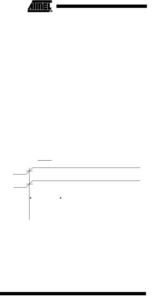
Table 6. Number of Watchdog Oscillator Cycles(1)
BODLEVEL |
VCC Condition |
Time-out |
Number of Cycles |
Unprogrammed |
2.7V |
30 µs |
8 |
|
|
|
|
Unprogrammed |
2.7V |
130 µs |
32 |
|
|
|
|
Unprogrammed |
2.7V |
4.2 ms |
1K |
|
|
|
|
Unprogrammed |
2.7V |
67 ms |
16K |
|
|
|
|
Programmed |
4.0V |
10 µs |
8 |
|
|
|
|
Programmed |
4.0V |
35 µs |
32 |
|
|
|
|
Programmed |
4.0V |
5.8 ms |
4K |
|
|
|
|
Programmed |
4.0V |
92 ms |
64K |
|
|
|
|
|
Note: 1. The Bodlevel Fuse can be used to select start-up times even if the Brown-out Detec- |
|
tion is disabled (BODEN Fuse unprogrammed). |
Power-on Reset |
A Power-on Reset (POR) pulse is generated by an On-chip detection circuit. The detec- |
|
tion level is defined in Table 4. The POR is activated whenever VCC is below the |
|
detection level. The POR circuit can be used to trigger the Start-up Reset, as well as to |
|
detect a failure in supply voltage. |
|
A Power-on Reset (POR) circuit ensures that the device is reset from Power-on. Reach- |
|
ing the Power-on Reset threshold voltage invokes a delay counter, which determines |
|
the delay, for which the device is kept in RESET after VCC rise. The Time-out Period of |
|
the delay counter can be defined by the user through the CKSEL Fuses. The different |
|
selections for the delay period are presented in Table 5. The RESET signal is activated |
|
again, without any delay, when the VCC decreases below detection level. |
Figure 25. MCU Start-up, RESET Tied to VCC.
|
VCC |
|
|
VPOT |
|
|||||
|
|
|
|
|
|
|
|
|||
|
|
|
|
|
|
VRST |
|
|||
|
RESET |
|
|
|||||||
|
|
|
|
|
|
|
|
|||
TIME-OUT |
|
|
|
tTOUT |
|
|
|
|||
|
|
|
|
|
|
|||||
|
|
|
||||||||
INTERNAL |
|
|
|
|
|
|
|
|||
|
|
|
|
|
|
|
||||
RESET |
|
|
|
|
|
|
|
|
||
26 ATmega163(L)
1142E–AVR–02/03
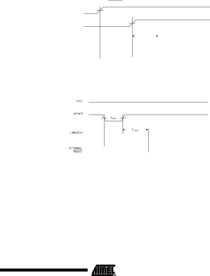
 ATmega163(L)
Figure 26. MCU Start-up, RESET Extended Externally
|
|
|
|
|
|
|
|
|
|
VPOT |
||||||||||||||
|
|
|
|
VCC |
||||||||||||||||||||
|
|
|
|
|
|
|
|
|
|
|
|
|
VRST |
|||||||||||
|
|
|
|
|
|
|
|
|
||||||||||||||||
|
|
|
RESET |
|||||||||||||||||||||
|
|
|
|
|
|
|
|
|
|
|
|
|
|
|
tTOUT |
|
|
|
|
|
||||
|
|
|
|
|
|
|
|
|
|
|
|
|
|
|
|
|
|
|
||||||
|
|
|
|
|
|
|
|
|
|
|
|
|
|
|
||||||||||
|
TIME-OUT |
|
|
|
||||||||||||||||||||
|
|
|
|
|
|
|
|
|
|
|
|
|
|
|
|
|
|
|
||||||
|
INTERNAL |
|
|
|
|
|
|
|
|
|
|
|
|
|
|
|
|
|||||||
External Reset |
|
RESET |
|
|
|
|
|
|
|
|
|
|
|
|
|
|
|
|
||||||
|
|
|
|
|
|
|
|
|
|
|
|
|
|
|
|
|
|
|
|
|
|
|
|
|
An External Reset is generated by a low level on the RESET pin. Reset pulses longer |
||||||||||||||||||||||||
|
than 500 ns will generate a Reset, even if the clock is not running. Shorter pulses are |
|||||||||||||||||||||||
|
not guaranteed to generate a Reset. When the applied signal reaches the Reset |
|||||||||||||||||||||||
|
Threshold Voltage – VRST on its positive edge, the delay timer starts the MCU after the |
|||||||||||||||||||||||
|
Time-out Period tTOUT has expired. |
|||||||||||||||||||||||
|
Figure 27. External Reset During Operation |
|||||||||||||||||||||||
|
|
|
|
|
|
|
|
|
|
|
|
|
|
|
|
|
|
|
|
|
|
|
|
|
|
|
|
|
|
|
|
|
|
|
|
|
|
|
|
|
|
|
|
|
|
|
|
|
|
|
|
|
|
|
|
|
|
|
|
|
|
|
|
|
|
|
|
|
|
|
|
|
|
|
|
|
|
|
|
|
|
|
|
|
|
|
|
|
|
|
|
|
|
|
|
|
|
|
|
|
|
|
|
|
|
|
|
|
|
|
|
|
|
|
|
|
|
|
|
|
|
|
|
|
|
|
|
|
|
|
|
|
|
|
|
|
|
|
|
|
|
|
|
|
|
|
|
|
|
|
|
|
|
|
|
|
|
|
|
|
|
|
|
|
|
|
|
|
|
|
|
|
|
|
|
|
|
|
|
|
|
|
|
|
|
|
|
|
|
|
|
|
|
|
|
|
|
|
|
Brown-out Detection |
ATmega163 has an On-chip Brown-out Detection (BOD) circuit for monitoring the VCC |
|
level during the operation. The BOD circuit can be enabled/disabled by the fuse |
|
BODEN. When the BOD is enabled (BODEN programmed), and VCC decreases to a |
|
value below the trigger level, the Brown-out Reset is immediately activated. When VCC |
|
increases above the trigger level, the Brown-out Reset is deactivated after a delay. The |
|
delay is defined by the user in the same way as the delay of POR signal, in Table 5. The |
|
trigger level for the BOD can be selected by the fuse BODLEVEL to be 2.7V |
|
(BODLEVEL unprogrammed), or 4.0V (BODLEVEL programmed). The trigger level has |
|
a hysteresis of 50 mV to ensure spike free Brown-out Detection. |
|
The BOD circuit will only detect a drop in VCC if the voltage stays below the trigger level |
|
for longer than 9 µs for trigger level 4.0V, 21 µs for trigger level 2.7V (typical values). |
27
1142E–AVR–02/03
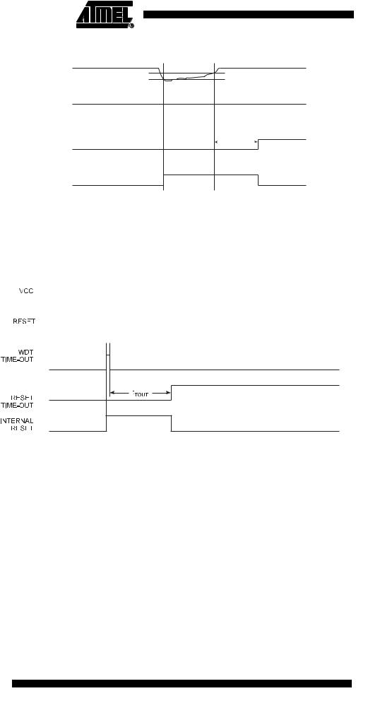
Figure 28. Brown-out Reset During Operation
VCC |
VBOT+ |
|
VBOT- |
RESET |
|
TIME-OUT |
tTOUT |
INTERNAL |
|
RESET |
|
|
The hysteresis on VBOT: VBOT+ = VBOT + 25 mV, VBOT- = VBOT - 25 mV |
||||
Watchdog Reset |
When the Watchdog times out, it will generate a short reset pulse of 1 XTAL cycle dura- |
||||
|
tion. On the falling edge of this pulse, the delay timer starts counting the Time-out Period |
||||
|
tTOUT. Refer to page 60 for details on operation of the Watchdog Timer. |
||||
|
Figure 29. Watchdog Reset During Operation |
||||
|
|
|
|
|
|
|
|
|
|
|
|
|
|
|
|
|
|

 1 CK Cycle
MCU Status Register – |
The MCU Status Register provides information on which reset source caused an MCU |
|||||||||
MCUSR |
Reset. |
|
|
|
|
|
|
|
|
|
|
Bit |
7 |
6 |
5 |
4 |
3 |
2 |
1 |
0 |
|
|
|
|
|
|
|
|
|
|
|
|
|
$34 ($54) |
– |
– |
– |
– |
WDRF |
BORF |
EXTRF |
PORF |
MCUSR |
|
|
|
|
|
|
|
|
|
|
|
|
Read/Write |
R |
R |
R |
R |
R/W |
R/W |
R/W |
R/W |
|
|
Initial Value |
0 |
0 |
0 |
0 |
|
See Bit Description |
|||
• Bits 7..4 – Res: Reserved Bits
These bits are reserved bits in the ATmega163 and always read as zero.
• Bit 3 – WDRF: Watchdog Reset Flag
This bit is set if a Watchdog Reset occurs. The bit is reset by a Power-on Reset, or by writing a logic zero to the Flag.
28 ATmega163(L)
1142E–AVR–02/03

 ATmega163(L)
|
• Bit 2 – BORF: Brown-out Reset Flag |
|
This bit is set if a Brown-out Reset occurs. The bit is reset by a Power-on Reset, or by |
|
writing a logic zero to the Flag. |
|
• Bit 1 – EXTRF: External Reset Flag |
|
This bit is set if an External Reset occurs. The bit is reset by a Power-on Reset, or by |
|
writing a logic zero to the flag. |
|
• Bit 0 – PORF: Power-on Reset Flag |
|
This bit is set if a Power-on Reset occurs. The bit is reset only by writing a logic zero to |
|
the flag. |
|
To make use of the Reset Flags to identify a reset condition, the user should read and |
|
then reset the MCUSR as early as possible in the program. If the register is cleared |
|
before another reset occurs, the source of the reset can be found by examining the |
|
Reset Flags. |
Internal Voltage Reference |
ATmega163 features an internal bandgap reference with a nominal voltage of 1.22V. |
|
This reference is used for Brown-out Detection, and it can be used as an input to the |
|
Analog Comparator and ADC. The 2.56V reference to the ADC is also generated from |
|
the internal bandgap reference. |
Voltage Reference Enable |
To save power, the reference is not always turned on. The reference is on during the fol- |
Signals and Start-up Time |
lowing situations: |
|
1. When the BOD is enabled (by programming the BODEN Fuse) |
|
2. When the bandgap reference is connected to the Analog Comparator (by setting |
|
the ACBG bit in ACSR). |
|
3. When the ADC is enabled. |
|
Thus, when the BOD is not enabled, after setting the ACBG bit, the user must always |
|
allow the reference to start up before the output from the Analog Comparator is used. |
|
The bandgap reference uses typically 10 µA, and to reduce power consumption in |
|
Power-down mode, the user can avoid the three conditions above to ensure that the ref- |
|
erence is turned off before entering Power-down mode. |
Interrupt Handling |
The ATmega163 has two 8-bit Interrupt Mask Control Registers: GIMSK – General |
|
Interrupt Mask Register and TIMSK – Timer/Counter Interrupt Mask Register. |
|
When an interrupt occurs, the Global Interrupt Enable I-bit is cleared (zero) and all inter- |
|
rupts are disabled. The user software must set (one) the I-bit to enable nested |
|
interrupts. The I-bit is set (one) when a Return from Interrupt instruction – RETI – is |
|
executed. |
|
When the Program Counter is vectored to the actual Interrupt Vector in order to execute |
|
the interrupt handling routine, hardware clears the corresponding flag that generated the |
|
interrupt. Some of the interrupt flags can also be cleared by writing a logic one to the flag |
|
bit position(s) to be cleared. |
|
If an interrupt condition occurs when the corresponding interrupt enable bit is cleared |
|
(zero), the Interrupt Flag will be set and remembered until the interrupt is enabled, or the |
|
flag is cleared by software. |
29
1142E–AVR–02/03

Interrupt Response Time
The General Interrupt Mask
Register – GIMSK
If one or more interrupt conditions occur when the Global Interrupt Enable bit is cleared (zero), the corresponding interrupt flag(s) will be set and remembered until the Global Interrupt Enable bit is set (one), and will be executed by order of priority.
Note that external level interrupt does not have a flag, and will only be remembered for as long as the interrupt condition is present.
Note that the Status Register is not automatically stored when entering an interrupt routine and restored when returning from an interrupt routine. This must be handled by software.
The interrupt execution response for all the enabled AVR interrupts is four clock cycles minimum. After four clock cycles the Program Vector address for the actual interrupt handling routine is executed. During this four clock cycle period, the Program Counter (13 bits) is pushed onto the Stack. The vector is normally a jump to the interrupt routine, and this jump takes three clock cycles. If an interrupt occurs during execution of a multicycle instruction, this instruction is completed before the interrupt is served. If an interrupt occurs when the MCU is in sleep mode, the interrupt execution response time is increased by four clock cycles.
A return from an interrupt handling routine takes four clock cycles. During these four clock cycles, the Program Counter (two bytes) is popped back from the Stack, the Stack Pointer is incremented by two, and the I Flag in SREG is set. When AVR exits from an interrupt, it will always return to the main program and execute one more instruction before any pending interrupt is served.
Bit |
7 |
6 |
5 |
4 |
3 |
2 |
1 |
0 |
|
$3B ($5B) |
INT1 |
INT0 |
– |
– |
– |
– |
– |
– |
GIMSK |
|
|
|
|
|
|
|
|
|
|
Read/Write |
R/W |
R/W |
R |
R |
R |
R |
R |
R |
|
Initial Value |
0 |
0 |
x |
0 |
0 |
0 |
0 |
0 |
|
• Bit 7 – INT1: External Interrupt Request 1 Enable
When the INT1 bit is set (one) and the I-bit in the Status Register (SREG) is set (one), the external pin interrupt is activated. The Interrupt Sense Control1 bits 1/0 (ISC11 and ISC10) in the MCU general Control Register (MCUCR) define whether the external interrupt is activated on rising and/or falling edge of the INT1 pin or level sensed. Activity on the pin will cause an interrupt request even if INT1 is configured as an output. The corresponding interrupt of External Interrupt Request 1 is executed from program memory address $004. See also “External Interrupts”.
• Bit 6 – INT0: External Interrupt Request 0 Enable
When the INT0 bit is set (one) and the I-bit in the Status Register (SREG) is set (one), the external pin interrupt is activated. The Interrupt Sense Control0 bits 1/0 (ISC01 and ISC00) in the MCU General Control Register (MCUCR) define whether the external interrupt is activated on rising or falling edge of the INT0 pin or level sensed. Activity on the pin will cause an interrupt request even if INT0 is configured as an output. The corresponding interrupt of External Interrupt Request 0 is executed from Program Memory address $002. See also “External Interrupts.”
• Bits 5 – Res: Reserved Bits
This bit is reserved in the ATmega163 and the read value is undefined.
30 ATmega163(L)
1142E–AVR–02/03
Loading...