


ATmega161-4JI
Table of contents
 Loading...
ATMEL ATmega161-4JI, ATmega161-4JC, ATmega161-4AI, ATmega161-4AC, ATmega161-8PI Datasheet
...
Features
• High-performance, Low-power AVR
• Advanced RISC Architecture
– 130 Powerful Instructions - Most Single Clock Cycle Execution
– 32 x 8 General Purpose Working Registers
– Fully Static Operation
– Up to 8 MIPS Throughput at 8 MHz
– On-chip 2-cycle Multiplier
• Program and Data Memories
– 16K Bytes of Nonvolatile In-System Programmable Flash
Endurance: 1,000 Write/Erase Cycles
– Optional Boot Code Memory with Independent Lock Bits
Self-programming of Program and Data Memories
– 512 Bytes Nonvolatile In-System Programmable EEPROM
Endurance: 100,000 Write/Erase Cycles
– 1K Bytes Internal SRAM
– Programming Lock for Software Security
• Peripheral Features
– Two 8-bit Timer/Counters with Separate Prescaler and PWM
– Expanded 16-bit Timer/Counter System with Separate Prescaler, Compare,
Capture Modes and Dual 8-, 9- or 10-bit PWM
– Dual Programmable Serial UARTs
– Master/Slave SPI Serial Interface
– Real Time Counter with Separate Oscillator
– Programmable Watchdog Timer with Separate On-chip Oscillator
– On-chip Analog Comparator
• Special Microcontroller Features
– Power-on Reset and Programmable Brown-out Detection
– External and Internal Interrupt Sources
– Three Sleep Modes: Idle, Power Save and Power-down
• I/O and Packages
– 35 Programmable I/O Lines
– 40-pin PDIP, 44-pin PLCC and TQFP
• Operating Voltages
– 2.7V - 5.5V (ATmega161L), 4.0V - 5.5V (ATmega161)
• Speed Grades
– 0 - 4 MHz (ATmega161L), 0 - 8 MHz (ATmega161)
• Commercial and Industrial Temperature Ranges
®
8-bit Microcontroller
8-bit
Microcontroller
with 16K Bytes
In-System
Programmable
Flash
ATmega161
ATmega161L
Advance
Information
Rev. 1228A–08/99
1
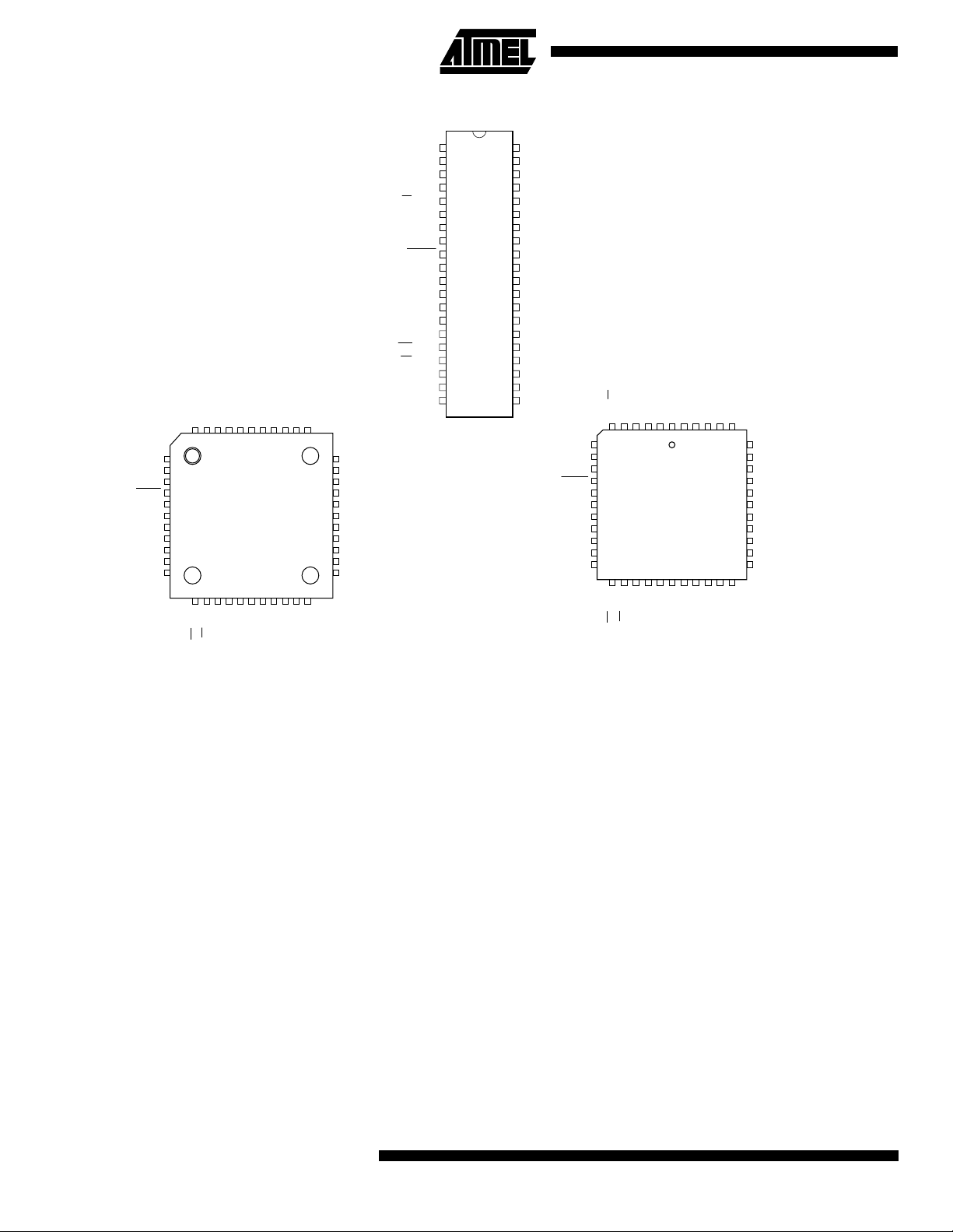
Pin Configurations
1
2
3
4
5
6
7
8
9
10
11
33
32
31
30
29
28
27
26
25
24
23
(MOSI) PB5
(MISO) PB6
(SCK) PB7
RESET
(RXD0) PD0
NC*
(TXD0) PD1
(INT0) PD2
(INT1) PD3
(TOSC1) PD4
(OCIA/TOSC2) PD5
PA4 (AD4)
PA5 (AD5)
PA6 (AD6)
PA7 (AD7)
PE0 (ICP/INT2)
NC*
PE1 (ALE)
PE2 (OC1B)
PC7 (A15)
PC6 (A14)
PC5 (A13)
4443424140393837363534
1213141516171819202122
(WR) PD6
(RD) PD7
XTAL2
XTAL1
GND
NC*
(A8) PC0
(A9) PC1
(A10) PC2
(A11) PC3
(A12) PC4
PB4 (SS)
PB3 (TXD1/AIN1)
PB2 (RXD1/AIN0)
PB1 (OC2/T1)
PB0 (OC0/T0)
NC*
VCC
PA0 (AD0)
PA1 (AD1)
PA2 (AD2)
PA3 (AD3)
* NC = Do not connect
(Can be used in future devices)
PDIP
TQFP
(OC0/T0) PB0
(OC2/T1) PB1
(RXD1/AIN0) PB2
(TXD1/AIN1) PB3
(SS) PB4
(MOSI) PB5
(MISO) PB6
(SCK) PB7
RESET
(RXD0) PD0
(TXD0) PD1
(INT0) PD2
(INT1) PD3
(TOSC1) PD4
(OC1A/TOSC2) PD5
(WR) PD6
(RD) PD7
XTAL2
XTAL1
GND
1
2
3
4
5
6
7
8
9
10
11
12
13
14
15
16
17
18
19
20
40
VCC
39
PA0 (AD0)
38
PA1 (AD1)
37
PA2 (AD2)
36
PA3 (AD3)
35
PA4 (AD4)
34
PA5 (AD5)
33
PA6 (AD6)
32
PA7 (AD7)
31
PE0 (ICP/INT2)
30
PE1 (ALE)
29
PE2 (OC1B)
28
PC7 (A15)
27
PC6 (A14)
26
PC5 (A13)
25
PC4 (A12)
24
PC3 (A11)
23
PC2 (A10)
22
PC1 (A9)
21
PC0 (A8)
(MOSI) PB5
(MISO) PB6
(SCK) PB7
(RXD0) PD0
(TXD0) PD1
(INT0) PD2
(INT1) PD3
(TOSC1) PD4
(OC1A/TOSC2) PD5
RESET
NC*
PLCC
PB4 (SS)
PB3 (TXD1/AIN1)
PB2 (RXD1/AIN0)
PB1 (OC2/T1)
PB0 (OC0/T0)
NC*
VCC
PA0 (AD0)
65432
7
8
9
10
11
12
13
14
15
16
17
1819202122232425262728
(RD) PD7
(WR) PD6
XTAL2
XTAL1
GND
1
NC*
4443424140
(A8) PC0
(A9) PC1
PA1 (AD1)
PA2 (AD2)
PA3 (AD3)
39
PA4 (AD4)
38
PA5 (AD5)
37
PA6 (AD6)
36
PA7 (AD7)
35
PE0 (ICP/INT2)
34
NC*
33
PE1 (ALE)
32
PE2 (OC1B)
31
PC7 (A15)
30
PC6 (A14)
PC5 (A13)
29
* NC = Do not connect
(Can be used in future devices)
(A10) PC2
(A11) PC3
(A12) PC4
Description
The ATmega161 is a low-power CMOS 8-bit microcontroller based on the AVR RISC architec ture. B y execu ting po werful
instructions in a single clock cycl e, the ATme ga161 achi eves throu ghputs ap proach ing 1 MIP S per MHz allo wing the system designer to op timi ze p ower c ons umption ve rsu s pro cessi ng s peed .The A VR
32 general purpose workin g registers. All the 32 registers are directl y connected to the Arithm etic Logic Unit (ALU),
allowing two independent registers to be accessed in one single instruction executed in one clock cycle. The resulting
architecture is more code efficient while achieving throughputs up to ten times faster than conventional CISC
microcontrollers.
The ATmega161 provides the followi ng features: 16K bytes of In-System- or Self-programmable Flash, 512 bytes
EEPROM, 1K bytes SR AM , 35 general purpose I/O l ine s, 32 g ener a l pu rpos e wor king registers, Real Time Cou nter , th re e
flexible timer/counters with compare modes, internal and external interrupts, two programmable serial UARTs, programmable Watchdog Timer with internal oscillator, an SPI serial port and three software selectable power saving modes. The Idle
mode stops the CPU while a llow ing t he S RAM, timer /cou nters, SPI port and interr upt s ystem to c ontin ue fu ncti oning. T he
power-down mode s aves the registe r an d SRA M co ntents but freez es the osci llato r, dis ablin g all othe r ch ip fu nctio ns unti l
the next external interrupt or hardware reset. In Power Save mode, the timer oscillator continues to run, allowing the user to
maintain a timer base while the rest of the device is sleeping.
The device is manufac tured using At mel’s h igh density nonv olati le memor y t echno logy. T he o n-chip Flas h pro gram memory can be reprogrammed using the self-programming capability through the bootblock, using an ISP through the SPI-port,
or by using a conventional nonvolatile memory programmer. By combining an enhanced RISC 8-bit CPU with In-System
Programmable Flash on a monolithic chip, the Atmel ATmega161 is a powerful microcontroller that provides a highly
flexible and cost effective solution to many embedded control applications.
The ATmega161 AVR
macro assemblers, program debugger/simulators, in-circuit emulators, and evaluation kits.
2
core combines a rich instruction set with
is supported with a full suite of program and system development tools including: C compilers,
ATmega161(L)
Block Diagram
Figure 1. The ATmega161 Block Diagram
ATmega161(L)
VCC
GND
PORTA DRIVERS
DATA REGISTER
PORTA
PROGRAM
COUNTER
PROGRAM
FLASH
INSTRUCTION
REGISTER
INSTRUCTION
DECODER
PA0-PA7
DATA DIR.
REG. PORTA
STACK
POINTER
SRAM
GENERAL
PURPOSE
REGISTERS
X
Y
Z
DATA REGISTER
8-BIT DATA BUS
PORTC DRIVERS
PORTC
INTERNAL
OSCILLATOR
WATCHDOG
TIMER
MCU CONTROL
REGISTER
TIMER/
COUNTERS
INTERRUPT
UNIT
PC0-PC7
DATA DIR.
REG. PORTC
OSCILLATOR
TIMING AND
CONTROL
XTAL1
XTAL2
RESET
ARATOR
ANALOG
COMP
-
+
CONTROL
LINES
PROGRAMMING
LOGIC
DATA REGISTER
PORTB
STATUS
REGISTER
DATA DIR.
REG. PORTB
PORTB DRIVERS
PB0 - PB7
ALU
SPI
DATA REGISTER
PORTD
PORTD DRIVERS
EEPROM
UARTS
REG. PORTD
PD0 - PD7
DATA DIR.
DATA REG.
PORTE
PORTE DRIVERS
PE0 - PE2
DATA DIR
REG. PORTE
3

Pin Descriptions
VCC
Supply voltage
GND
Ground
Port A (PA7..PA0)
Port A is an 8-bit bidirectional I/O port. Port pins can provide internal pull-up resistors (selected for each bit). The Port A
output buffers ca n sink 20 mA and c an drive LED disp lays dir ectly. When pi ns PA0 to PA7 ar e used as inputs and are
externally pulled low, they will source current if the internal pull- up resistors are activated. The Port A pins are tri-stated
when a reset condition becomes active, even if the clock is not running.
Port A serves as Multiplexed Address/Data port when using external memory interface.
Port B (PB7..PB0)
Port B is an 8 -bit bi dir ectional I/O por t with inte rnal pu ll- up res istors . The Port B o utput buffer s can sink 20 mA. As inp uts,
Port B pins that are externally pulled low will source current if the pull-up resistors are activated. The Port B pins are
tri-stated when a reset condition becomes active, even if the clock is not running.
Port B also serves the functions of various special features of the ATmega161 as listed on page 80.
Port C (PC7..PC0)
Port C is an 8-bit bidire ctiona l I/O po rt wit h inter nal pull-up resi stors. The Port C ou tpu t buffers can si nk 20 mA. A s inputs ,
Port C pins that are externally pulled low will source current if the pull-up resistors are activated. The Port C pins are
tri-stated when a reset condition becomes active, even if the clock is not running.
Port C also serves as Address high output when using external memory interface.
Port D (PD7..PD0)
Port D is an 8-bit bidire ctiona l I/O po rt wit h inter nal pull-up resi stors. The Port D ou tpu t buffers can si nk 20 mA. A s inputs ,
Port D pins that are externally pulled low will source current if the pull-up resistors are activated. The Port D pins are
tri-stated when a reset condition becomes active, even if the clock is not running.
Port D also serves the functions of various special features of the ATmega161 as listed on page 87.
Port E (PE2..PE0)
Port E is a 3-bit bidirectional I/O port with internal pull-up resistors. The Port E output buffers can sink 20 mA. As inputs,
Port E pins that are externally pulled low will source current if the pull-up resistors are activated. The Port E pins are
tri-stated when a reset condition becomes active, even if the clock is not running.
Port E also serves the functions of various special features of the ATmega161 as listed on page 93.
RESET
Reset input. A low level on thi s pin for more than 500 ns will generate a res et, even if the clock i s not running. Sho rter
pulses are not guaranteed to generate a reset.
XTAL1
Input to the inverting oscillator amplifier and input to the internal clock operating circuit.
XTAL2
Output from the inverting oscillator amplifier
4
ATmega161(L)
ATmega161(L)
Crystal Oscillator
XTAL1 and XTAL2 are input and output, respectively, of an inverting amplifier which can be configured for use as an
on-chip oscillator, as shown in Figure 2. Either a quartz crystal or a ceramic resonator may be used. To drive the device
from an external clock source, XTAL2 should be left unconnected while XTAL1 is driven as shown in Figure 3.
Figure 2. Oscillator Connections
MAX 1 HC BUFFER
HC
C2
C1
Note: When using the MCU Oscillator as a clock for an external device, an HC buffer should be connected as indicated in the figure.
Figure 3. External Clock Drive Configuration
XTAL2
XTAL1
GND
5
Architectural Overview
The fast-access register file concept contains 32 x 8-bit general purpose working registers with a single clock cycle access
time. This means th at d urin g on e s in gl e cloc k cyc le, one Arithmetic Logic Uni t ( ALU) op er ation i s ex ecute d. T wo ope ra nds
are output from the register file, the operation is executed, and the result is stored back in the register file – in one clock
cycle.
Six of the 32 registers can be used as three 16-bits indirect address register pointers for Data Space addressing – enabling
efficient address cal cula tions. One of the three addre ss po inters i s also used a s the ad dres s pointer for the const ant tabl e
look up function. These added function registers are the 16-bits X-register, Y-register and Z-register.
Figure 4. The ATmega161 AVR
RISC Architecture
AVR
8K x 16
Program
Memory
Instruction
Register
Instruction
Decoder
Control Lines
ATmega161 Architecture
Program
Counter
Direct Addressing
Indirect Addressing
Data Bus 8-bit
Status
and Control
32 x 8
General
Purpose
Registers
ALU
1024 x 8
Data
SRAM
Interrupt
Unit
SPI
Unit
Serial
UART0
Serial
UART1
8-bit
Timer/Counter
with PWM
and RTC
16-bit
Timer/Counter
with PWM
8-bit
Timer/Counter
with PWM
512 x 8
EEPROM
32
I/O Lines
6
ATmega161(L)
Watchdog
Timer
Analog
Comparator

ATmega161(L)
The ALU supports arithmetic and logic functions between registers or between a constant and a register. Single register
operations are also executed in the ALU. Figure 4 shows the ATmega161 AVR
RISC microcontroller architecture.
In addition to the register operation, the conventional memory addressing modes can be used on the register file as well.
This is enabled by the fa ct th at the re giste r file is assig ned t he 32 lowe rmost Dat a Spa ce add resses ( $00 - $ 1F), allo wing
them to be accessed as though they were ordinary memory locations.
The I/O memory spac e contai ns 64 a ddresses for CPU peripheral function s as Contr ol Regis ters, Tim er/Counters , and
other I/O functions. The I/O M emo ry c an be a cc ess ed d ir ectly , o r a s the D ata S pa ce loc at ion s f oll owing thos e o f the register file, $20 - $5F.
The AVR
uses a Harvard architecture concept – with separate memories and buses for program and data. The program
memory is executed with a two stage pipeline. While one instruction is being executed, the next instruction is pre-fetched
from the program memory. This conc ept enable s instru ctio ns to be executed in every cl ock cyc le. The program memory is
Self-programmable Flash memory.
With the jump and call in struc tions , the whol e 8K word ad dress sp ace is directl y acce ssed. Mo st AVR
instructio ns hav e a
single 16-bit word format. Every program memory address contains a 16- or 32-bit instruction.
During interrupts and su broutine call s, the r etur n addres s pr ogram co unte r (PC) is stored on the sta ck. The stac k is effe c-
tively allocate d in the ge neral data SR AM, an d consequen tly the st ack size is only limi ted by the total SRAM size and th e
usage of the SRAM. All us er progra ms must initialize the S P (Stack P ointer) in the res et routin e (befor e subroutin es or
interrupts are executed). The 16-bit stack pointer is read/write accessible in the I/O space.
The 1K bytes data SRAM can be easi ly accessed through the five different addressing modes s upported in the AVR
architecture.
The memory spaces in the AVR
architecture are all linear and regular memory maps.
7
Figure 5. Memory Maps
Program Memory
Data Memory
Program Flash
(8K x 16)
$000
$1FFF
32 Gen. Purpose
Working Registers
64 I/O Registers
Internal SRAM
(1024 x 8)
External SRAM
(0-63K x 8)
$0000
$001F
$0020
$005F
$0060
$045F
$0460
$FFFF
A flexible interrupt module has its control registers in the I/O space with an additional global interrupt enable bit in the status
register. All the different interrupts have a separate interrupt vector in the interrupt vector table at the beginning of the
program me mory. The di fferen t interr upts hav e prior ity in acco rdance with th eir inte rrupt v ector p ositi on. The lower the
interrupt vector address, the higher the priority.
8
ATmega161(L)
General Purpose Register File
Figure 6 shows the structure of the 32 general purpose working registers in the CPU.
Figure 6. AVR
CPU General Purpose Working Registers
70Addr.
R0 $00
R1 $01
R2 $02
…
R13 $0D
General R14 $0E
Purpose R15 $0F
Working R16 $10
Registers R17 $11
…
R26 $1A X-register low byte
R27 $1B X-register high byte
R28 $1C Y-register low byte
R29 $1D Y-register high byte
R30 $1E Z-register low byte
R31 $1F Z-register high byte
ATmega161(L)
All the register operat ing instructi ons in the instruction s et have dir ect and s ingle cycle acc ess to all r egisters. T he only
exceptions are the five constant arithmetic and logic instructions SBCI, SUBI, CPI, ANDI, and ORI between a constant and
a register, and the LDI ins truc ti on for l oad i mm edi ate c on stant da ta. T he se instr uct io ns appl y to the secon d hal f of th e r egisters in the regis ter file – R1 6..R31 . The gen eral SB C, SUB, CP, AN D, and OR, a nd all ot her op erations between two
registers or on a single register apply to the entire register file.
As shown in Figu re 6, each regi ster is als o as signe d a da ta mem ory add ress , map ping t hem direct ly i nto the first 32 loc ations of the user Data Space. Although not being physicall y implemented as SRAM locati ons, this memory organiza tion
provides great flexibility in access of the registers, as the X, Y and Z-registers can be set to index any register in the file.
X-register, Y-register, and Z-register
The registers R2 6..R31 have som e add ed fun ction s to their gener al p urpose usa ge. The se r egister s are addr ess p ointe rs
for indirect addressing of the Data Space. The three indirect address registers X, Y and Z are defined as:
Figure 7. X, Y and Z-registers
15 0
X-register 7 0 7 0
R27 ($1B) R26 ($1A)
15 0
Y-register 7 0 7 0
R29 ($1D) R28 ($1C)
15 0
Z-register 7 0 7 0
R31 ($1F) R30 ($1E)
In the different address ing mod es , thes e ad dres s r egi ster s h ave func ti ons as f ixed di s pla ce men t, aut oma tic inc r em ent an d
decrement (see the descriptions for the different instructions).
9
ALU – Arithmetic Logic Unit
The high-performance AVR ALU operates in direct connection with all the 32 general purpose working registers. Within a
single clock cy cl e, AL U ope r atio ns be tween r egi ster s in the re gis te r f ile ar e ex ec uted . The ALU operations are div i ded in to
three main catego ries – arithmetic, logica l, an d bit- func tions. A Tme ga161 does also p rovide a po werful mul tipli er sup porting both signed/unsigned multiplication and fractional format. See Instruction Set section for a detailed description.
Self-programmable Flash Program Memory
The ATmega161 contains 16K bytes on-chip Self- and In-System programmable Flash memory for program storage. Since
all instructions a re 16- or 32 -bit words, the Flash is or ga nized as 8K x 16. The Flas h me mory has an end ur ance of at least
1000 write/erase cycles. The ATmega161 Program Counter ( PC) is 13 bi ts wide, thus addressing the 819 2 program
memory locations.
See page 95 for a detailed description on Flash data downloading.
See page 11 for the different program memory addressing modes.
EEPROM Data Memory
The ATmega161 contains 512 bytes of data EEPROM memory. It is organized as a separate data space, in which single
bytes can be read and written. The EEPROM has an endurance of at least 100,000 write/erase cycles per location. The
interface between the EEPROM and the CPU is described on page 54 specifying the EEPROM address registers, the
EEPROM data register, and the EEPROM control register.
For the SPI data downloading, see page 109 for a detailed description.
Figure 8. SRAM Organization
Register File Data Address Space
R0 $0000
R1 $0001
R2 $0002
º º
R29 $001D
R30 $001E
R31 $001F
I/O Registers
$00 $0020
$01 $0021
$02 $0022
……
$3D $005D
$3E $005E
$3F $005F
Internal SRAM
$0060
$0061
º
$045E
$045F
10
ATmega161(L)

ATmega161(L)
SRAM Data Memory
Figure 8 shows how the ATmega161 SRAM Memory is organized.
The lower 1120 Data Memory locations address the Register file, the I/O Memory and the internal data SRAM. The first 96
locations address the Register File and I/O Memory, and the next 1K loc ations address the internal data SRAM. An
optional external data memory device can be placed in the same SRAM memory space. This memory device will occupy
the locations following the internal SRAM and up to as much as 64K - 1, depending on external memory size.
When the addresses acc essing the da ta memory sp ace exc eeds the int ernal data SRA M locati ons, the memor y device is
accessed using the same instructions as for the internal data SRAM access. When the internal data space is accessed, the
read and write strobe pins (RD
by setting the SRE bit in the MCUCR register. See “Interface to external memory” on page 72 for details.
Accessing external memory takes one additional clock cycle per byte compared to access of the internal SRAM. This
means that the commands LD, ST, LDS, STS, PUSH and PO P take one a dditional clock cycle. If the s tack is plac ed in
external memory, interr upts, subroutine call s and returns take two clock c ycles extra because the two-by te program
counter is pushed and popped. When external memory interface is used with wait state, two additional clock cycles is used
per byte. This ha s t he foll owin g effe ct : Dat a tr an sfe r in struc ti ons ta ke two ex tra c lo ck c y cl es, whereas interrupt, subr ou tin e
calls and returns will need four clock cycles more than specified in the instruction set manual.
The five different addressing modes for the data memory cover: Direct, Indirect with Displacement, Indirect, Indirect with
Pre-Decrement, and Indire ct with Pos t-Incre ment. In th e regist er file, regi sters R2 6 to R31 feat ure the indi rect add ressing
pointer registers.
The direct addressing reaches the entire data space.
The Indirect with Displacement mode features a 63 address locations reach from the base address given by the Y or
Z-register.
When using register indirect addressing modes with automatic pre-decrement and post-increment, the address registers X,
Y and Z are decremented and incremented.
The 32 general purpose wo rk in g regi st er s, 6 4 I/O regi ste rs an d the 1K bytes of internal data SRA M in the A T meg a161 ar e
all accessible through all these addressing modes.
See the next section for a detailed description of the different addressing modes.
and WR) are inactive during the whole access cycle. External memory operation is enabled
Program and Data Addressing Modes
The ATmega161 AVR RISC microcontroller supports powerful and efficient addressing modes for access to the program
memory (Flash) and data mem or y (SRA M, Regis ter F ile , and I/O Mem or y). T his se cti on de scr ibe s the diffe re nt add ress in g
modes supported by the AVR
simplify, not all figures show the exact location of the addressing bits.
architecture. In the figures, OP means the operation code part of the instruction word. T o
11
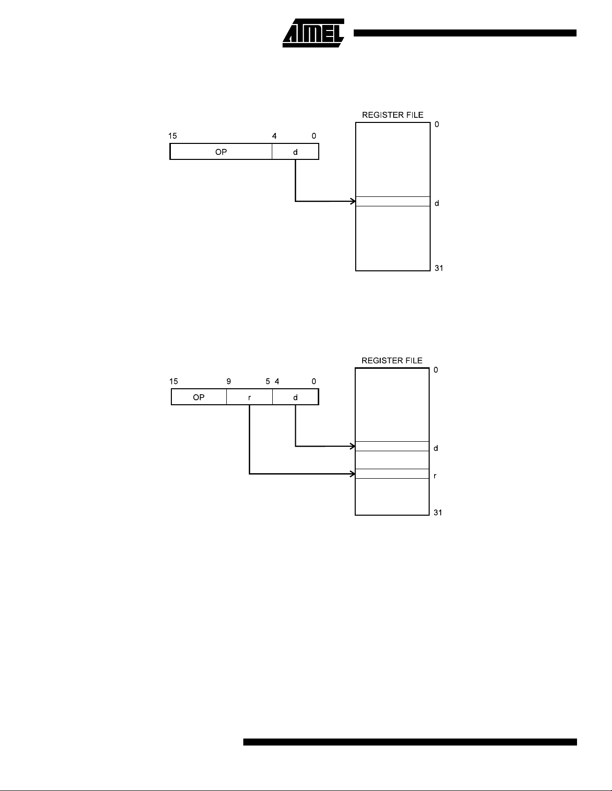
Register Direct, Single Register Rd
Figure 9. Direct Single Register Addressing
The operand is contained in register d (Rd).
Register Direct, Two Registers Rd and Rr
Figure 10. Direct Register Addressing, Two Registers
Operands are contained in register r (Rr) and d (Rd). The result is stored in register d (Rd).
12
ATmega161(L)
ATmega161(L)
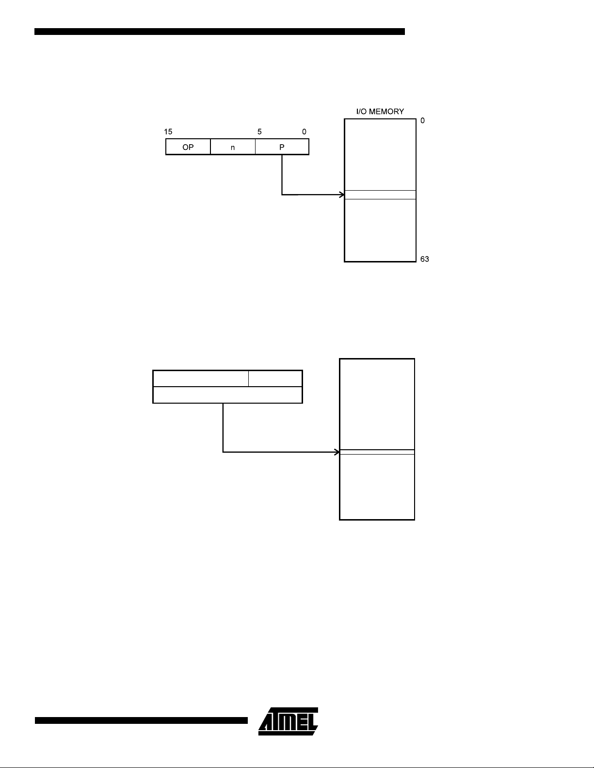
I/O Direct
Figure 11. I/O Direct Addressing
Operand address is contained in 6 bits of the instruction word. n is the destination or source register address.
Data Direct
Figure 12. Direct Data Addressing
Data Space
$0000
$FFFF
16 LSBs
20 19
16
31
OP Rr/Rd
15 0
A 16-bit Data Address is contained in the 1 6 LSBs of a two-word instructio n. Rd/Rr specify the destination or sourc e
register.
13
Data Indirect with Displacement Figure 13. Data Indirect with Displacement
15
Y OR Z - REGISTER
Data Space
$0000
0
15
OP an
05610
$FFFF
Operand address is the result of the Y or Z-register contents added to the address contained in 6 bits of the
instruction word.
Data Indirect
Figure 14. Data Indirect Addressing
Data Space
015
X, Y, OR Z - REGISTER
$0000
$FFFF
Operand address is the contents of the X, Y, or the Z-register.
14
ATmega161(L)
ATmega161(L)
Data Indirect with Pre-Decrement
Figure 15. Data Indirect Addressing with Pre-Decrement
Data Space
015
X, Y, OR Z - REGISTER
-1
The X, Y, or the Z-register is decremented before the operation. Operand address is the decremented contents of the X, Y,
or the Z-register.
$0000
$FFFF
Data Indirect with Post-Increment
Figure 16. Data Indirect Addressing with Post-Increment
Data Space
015
X, Y, OR Z - REGISTER
1
$0000
$FFFF
The X, Y, or the Z-register is inc r em ente d afte r th e ope ratio n. O per an d add ress is the con tent of the X , Y, o r th e Z-re g ister
prior to incrementing.
15

Constant Addressing Using the LPM Instruction
Figure 17. Code Memory Constant Addressing
PROGRAM MEMORY
$000
$1FFF
Constant byte addr ess is s pe cif ie d b y the Z-r eg ister c on tents. The 15 MSBs se le ct wor d add re ss ( 0 - 8K ), the LS B se le cts
low byte if cleared (LSB = 0) or high byte if set (LSB = 1).
Indirect Program Addressing, IJMP and ICALL
Figure 18. Indirect Program Memory Addressing
PROGRAM MEMORY
$000
$1FFF
Program execution continues at address contained by the Z-register (i.e. the PC is loaded with the contents of the
Z-register).
16
ATmega161(L)
ATmega161(L)
Relative Program Addressing, RJMP and RCALL
Figure 19. Relative Program Memory Addressing
PROGRAM MEMORY
Program execution continues at address PC + k + 1. The relative address k is -2048 to 2047.
Direct Program Addressing, JMP and CALL
$000
$1FFF
Figure 20. Direct Program Addressing
PROGRAM MEMORY
31
OP
15 0
21 20
16 LSBs
16
Program execution continues at the address immediate in the instruction words.
$0000
$1FFF
17
Memory Access Times and Instruction Execution Timing
This section describes the general access timing concepts for instruction execution and internal memory access.
The AVR
clock division is used.
Figure 21 shows the parallel instruction fetches and instructio n executions enabled by the Harvard architecture and the
fast-access register file concept. This is the basic pipelining concept to obtain up to 1 MIPS per MHz with the corresponding
unique results for functions per cost, functions per clocks, and functions per power-unit.
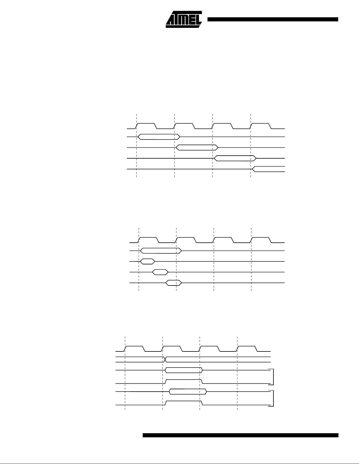
Figure 21. The Parallel Instruction Fetches and Instruction Executions
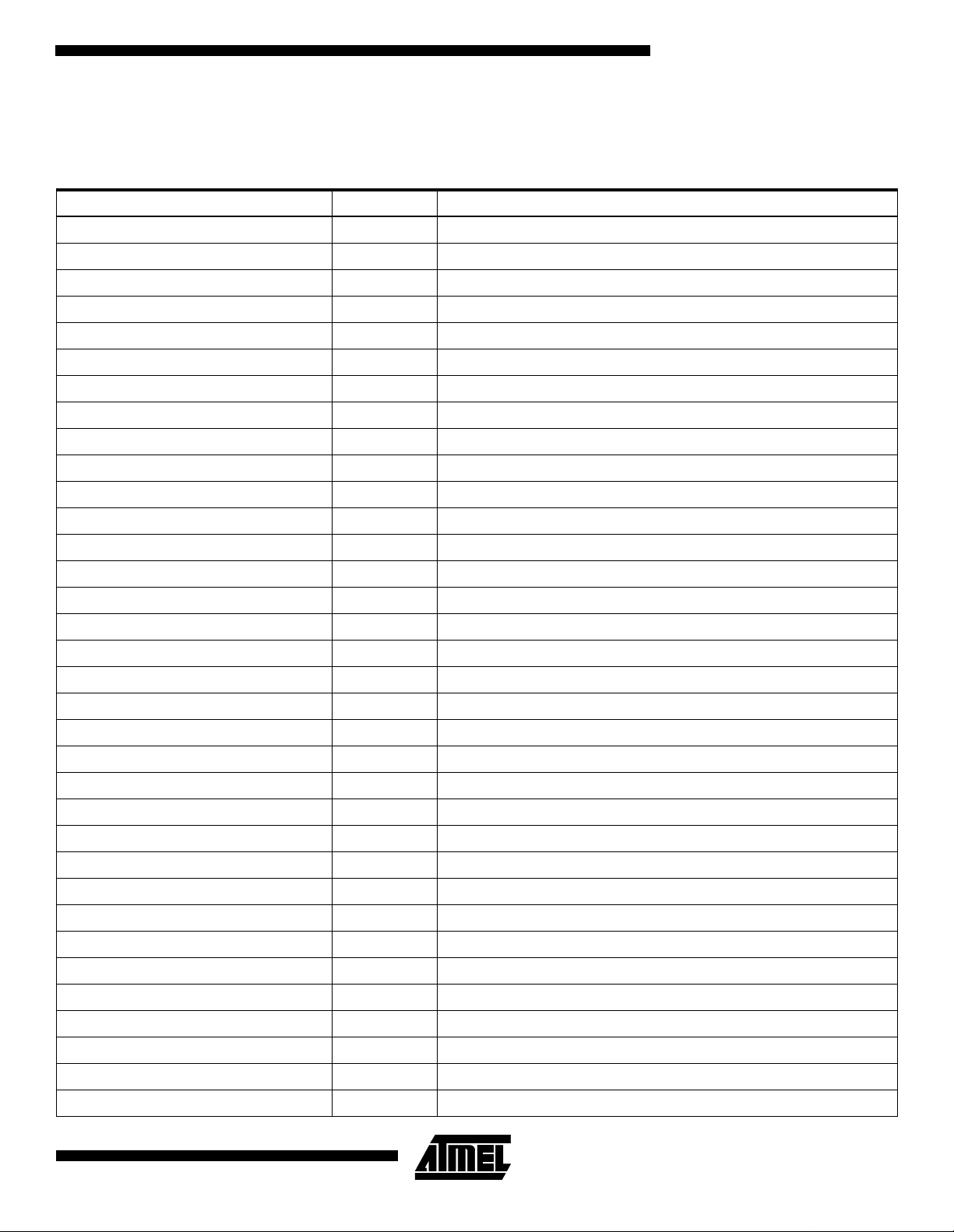
Figure 22 shows the internal timing concept for the register file. In a single clock cycle an ALU operation using two register
operands is executed, and the result is stored back to the destination register.
CPU is driven by the System Clock Ø, directly generated from the external clock crys tal for the chip. No in ternal
T1 T2 T3 T4
System Clock Ø
1st Instruction Fetch
1st Instruction Execute
2nd Instruction Fetch
2nd Instruction Execute
3rd Instruction Fetch
3rd Instruction Execute
4th Instruction Fetch
Figure 22. Single Cycle ALU Operation
T1 T2 T3 T4
System Clock Ø
Total Execution Time
Register Operands Fetch
ALU Operation Execute
Result Write Back
The internal data SRAM access is performed in two System Clock cycles as described in Figure 23.
Figure 23. On-chip Data SRAM Access Cycles
T1 T2 T3 T4
System Clock Ø
Address
Data
WR
Prev. Address
Address
Write
18
Data
RD
ATmega161(L)
Read
I/O Memory
The I/O space definition of the ATmega161 is shown in the following table:
Table 1. ATmega161 I/O Space
I/O Address (SRAM Address) Name Function
$3F($5F) SREG Status REGister
$3E ($5E) SPH Stack Pointer High
$3D ($5D) SPL Stack Pointer Low
$3B ($5B) GIMSK General Interrupt MaSK register
$3A ($5A) GIFR General Interrupt Flag Register
$39 ($59) TIMSK Timer/Counter Interrupt MaSK Register
$38 ($58) TIFR Timer/Counter Interrupt Flag Register
$37 ($57) SPMCR Store Program Memory Control Register
$36 ($56) EMCUCR Extended MCU general Control Register
$35 ($55) MCUCR MCU general Control Register
$34 ($54) MCUSR MCU general Status Register
ATmega161(L)
$33 ($53) TCCR0 Timer/Counter0 Control Register
$32 ($52) TCNT0 Timer/Counter0 (8-bit)
$31 ($51) OCR0 Timer/Counter0 Output Compare Register
$30 ($50) SFIOR Special Function IO Register
$2F ($4F) TCCR1A Timer/Counter1 Control Register A
$2E ($4E) TCCR1B Timer/Counter1 Control Register B
$2D ($4D) TCNT1H Timer/Counter1 High Byte
$2C ($4C) TCNT1L Timer/Counter1 Low Byte
$2B ($4B) OCR1AH Timer/Counter1 Output Compare RegisterA High Byte
$2A ($4A) OCR1AL Timer/Counter1 Output Compare RegisterA Low Byte
$29 ($49) OCR1BH Timer/Counter1 Output Compare RegisterB High Byte
$28 ($48) OCR1BL Timer/Counter1 Output Compare RegisterB Low Byte
$27 ($47) TCCR2 Timer/Counter2 Control Register
$26 ($46) ASSR Asynchronous mode StatuS Register
$25 ($45) ICR1H Timer/Counter1 Input Capture Register High Byte
$24 ($44) ICR1L Timer/Counter1 Input Capture Register Low Byte
$23 ($43) TCNT2 Timer/Counter2 (8-bit)
$22 ($42) OCR2 Timer/Counter2 Output Compare Register
$21 ($41) WDTCR Watchdog Timer Control Register
$20 ($40) UBRRHI UART Baud Register HIgh
$1F ($3F) EEARH EEPROM Address Register High
$1E ($3E) EEARL EEPROM Address Register Low
$1D ($3D) EEDR EEPROM Data Register
19
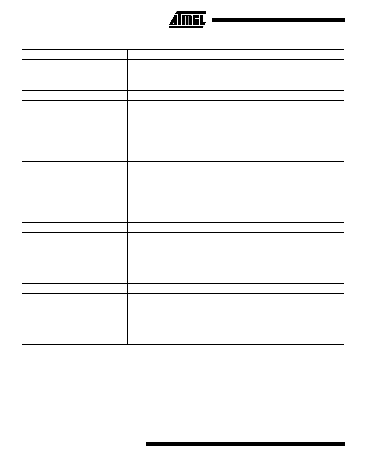
Table 1. ATmega161 I/O Space (Continued)
I/O Address (SRAM Address) Name Function
$1C ($3C) EECR EEPROM Control Register
$1B($3B) PORTA Data Register, Port A
$1A ($3A) DDRA Data Direction Register, Port A
$19 ($39) PINA Input Pins, Port A
$18 ($38) PORTB Data Register, Port B
$17 ($37) DDRB Data Direction Register, Port B
$16 ($36) PINB Input Pins, Port B
$15 ($35) PORTC Data Register, Port C
$14 ($34) DDRC Data Direction Register, Port C
$13 ($33) PINC Input Pins, Port C
$12 ($32) PORTD Data Register, Port D
$11 ($31) DDRD Data Direction Register, Port D
$10 ($30) PIND Input Pins, Port D
$0F ($2F) SPDR SPI I/O Data Register
$0E ($2E) SPSR SPI Status Register
$0D ($2D) SPCR SPI Control Register
$0C ($2C) UDR0 UART0 I/O Data Register
$0B ($2B) UCSR0A UART0 Control and Status Register
$0A ($2A) UCSR0B UART0 Control and Status Register
$09 ($29) UBRR0 UART0 Baud Rate Register
$08 ($28) ACSR Analog Comparator Control and Status Register
$07 ($27) PORTE Data Register, Port E
$06 ($26) DDRE Data Direction Register, Port E
$05 ($25) PINE Input Pins, Port E
$03 ($23) UDR1 UART1 I/O Data Register
$02 ($22) UCSR1A UART1 Control and Status Register
$01 ($21) UCSR1B UART1 Control and Status Register
$00 ($20) UBRR1 UART1 Baud Rate Register
Note: Reserved and unused locations are not shown in the table.
All ATmega161 I/Os and peripherals are placed in the I/O space. The I/O locations are accessed by the IN and OUT
instructions transfer ring data be tween the 32 gen eral purpose wor king regis ters an d the I/O space . I/O regist ers wit hin the
address range $00 - $1F are directl y bit-acces sible us ing the SBI and CBI instruct ions. In these re giste rs, the value of single bits can be check ed by using the SBIS and SB IC instructi ons. Refer to th e instructi on set chap ter for more details.
When using the I/O specific commands IN, OUT the I/O addresses $00 - $3F must be used. When addressing I/O registers
as SRAM, $20 must be added to this address. All I/O regi ster addresses throughout this document are shown with the
SRAM address in parentheses.
For compatibilit y with fut ur e d evi ce s, r es erve d b its s hou ld be wr itte n t o z er o if a cces s ed. Rese rve d I/ O mem or y addresses
should never be written.
20
ATmega161(L)
ATmega161(L)
Some of the status flags are cleared by writing a logical one to them. Note that the CBI and SBI instructions will operate on
all bits in the I/O regi ster , writing a on e back in to an y flag r ead as set, th us clea ring t he flag . The C BI and SB I instr ucti ons
work with registers $00 to $1F only.
The I/O and peripherals control registers are explained in the following sections.
Status Register – SREG
The AVR status register – SREG – at I/O space location $3F ($5F) is defined as:
Bit 76543210
$3F ($5F) I T H S V N Z C SREG
Read/Write R/W R/W R/W R/W R/W R/W R/W R/W
Initial value 0 0 0 0 0 0 0 0
Bit 7 - I: Global Interrupt Enable
•
The global interrup t enable bit must be set (one) for the interrup ts to be enable d. The indivi dual inter rupt enab le control is
then performed in separate control registers. If the global interrupt enable bit is cleared (zero), none of the interrupts are
enabled independent of the individual interrupt enable settings. The I-bit is cleared by hardware after an interrupt has
occurred, and is set by the RETI instruction to enable subsequent interrupts.
Bit 6 - T: Bit Copy Storage
•
The bit copy instructions BLD (Bit LoaD) and BST (Bit STore) use the T bit as source and destination for the operated bit. A
bit from a register in the regi ste r fi le can be copi ed i nto T by the B ST i ns tru ct ion , and a bit i n T can be c opied i nto a bit i n a
register in the register file by the BLD instruction.
Bit 5 - H: Half Carry Flag
•
The half carry flag H indicates a half carry in some arithmetic operations. See the Instruction Set Description for detailed
information.
Bit 4 - S: Sign Bit, S = N ⊕ V
•
The S-bit is always an exclusive or between the negative flag N and the two’s complement overflow flag V. See the Instruction Set Description for detailed information.
•
Bit 3 - V: Two’s Complement Overflow Flag
The two’s comp lement overflow flag V s upports two’s complement arithmetics. See the Instruction Set Description for
detailed information.
Bit 2 - N: Negative Flag
•
The negative flag N indicates a negative result after the different arithmetic and logic operations. See the Instruction Set
Description for detailed information.
Bit 1 - Z: Zero Flag
•
The zero flag Z indicates a zero result after the different arithmetic and logic operations. See the Instruction Set Description
for detailed information.
•
Bit 0 - C: Carry Flag
The carry flag C indicates a c arry in an arithmetic or logic operation. S ee the Instruction S et Description for detail ed
information.
Note that the status register is not automatically stored when entering an interrupt routine and restored when returning from
an interrupt routine. This must be handled by software.
21
Stack Pointer – SP
The ATmega161 Stac k Point er is impl emented as two 8-bit r egist ers in th e I/O sp ace lo ca tions $3E ($5E ) and $3D ($5D) .
As the ATmega161 supports up to 64KB memory, all 16 bits are used.
Bit 151413121110 9 8
$3E ($5E) SP15 SP14 SP13 SP12 SP11 SP10 SP9 SP8 SPH
$3D ($5D) SP7 SP6 SP5 SP4 SP3 SP2 SP1 SP0 SPL
76543210
Read/Write R/W R/W R/W R/W R/W R/W R/W R/W
R/W R/W R/W R/W R/W R/W R/W R/W
Initial value 0 0 0 0 0 0 0 0
00000000
The Stack Poin ter po ints to th e da ta SRA M s tack area whe re the Subr outi ne an d Inte rru pt St acks are loca ted. T his Sta ck
space in the d ata SRAM m ust be defi ned by the program before any subroutine calls ar e executed or interrupts are
enabled. The stack pointer must be set to point above $60. The Stack Pointer is decremented by one when data is pushed
onto the Stack with the PUSH instruction, and it is decremented by two when an address is pushed onto the Stack with
subroutine calls and interrupts. The Stack Pointer is incremented by one when data is popped from the Stack with the POP
instruction, and it is incremen ted by two when an addres s is popped from the Stack with return from subroutine RET or
return from interrupt RETI.
Reset and Interrupt Handling
The ATmega161 pr ovide s 20 d iff er ent int er rupt s ou rces . T h es e in terr up ts and the se par at e r ese t ve cto r, each hav e a s eparate program vector in the program memory space. All interrupts are assigned individual enable bits which must be set
(one) together with the I-bit in the status register in order to enable the interrupt.
The lowest addresses i n the pro gram memo ry space are automatica lly defined a s the Rese t and Inter rupt vector s. The
complete list of vectors is shown in Table 2. The list also determines the priority levels of the different interrupts. The lower
the address the higher is the priority level. RESET has the highest priority , and next is INT0 – the External Interrupt
Request 0 etc.
Table 2. Reset and Interrupt Vectors
Vector No. Program Address Source Interrupt Definition
1 $000 RESET External Pin, Power-on Reset, Brown-out Reset and Watchd og Re se t
2 $002 INT0 External Interrupt Request 0
3 $004 INT1 External Interrupt Request 1
4 $006 INT2 External Interrupt Request 2
5 $008 TIMER2 COMP Timer/Counter2 Compare Match
6 $00a TIMER2 OVF Timer/Counter2 Overflow
7 $00c TIMER1 CAPT Timer/Counter1 Capture Event
8 $00e TIMER1 COMPA Timer/Counter1 Compare Match A
9 $010 TIMER1 COMPB Timer/Counter1 Compare Match B
10 $012 TIMER1 OVF Timer/Counter1 Overflow
11 $014 TIMER0 COMP Timer/Counter0 Compare Match
12 $016 TIMER0 OVF Timer/Counter0 Overflow
13 $018 SPI, STC Serial Transfer Complete
14 $01a UART0, RX UART0, Rx Complete
15 $01c UART1, RX UART1, Rx Complete
22
ATmega161(L)
ATmega161(L)
Table 2. Reset and Interrupt Vectors (Continued)
Vector No. Program Address Source Interrupt Definition
16 $01e UART0, UDRE UART0 Data Register Empty
17 $020 UART1, UDRE UART1 Data Register Empty
18 $022 UART0, TX UART0, Tx Complete
19 $024 UART1, TX UART1, Tx Complete
20 $026 EE_RDY EEPROM Ready
21 $028 ANA_COMP Analog Comparator
The most typical and general program setup for the Reset and Interrupt Vector Addresses are:
Address Labels Code Comments
$000 jmp RESET ; Reset Handler
$002 jmp EXT_INT0 ; IRQ0 Handler
$004 jmp EXT_INT1 ; IRQ1 Handler
$006 jmp EXT_INT2 ; IRQ2 Handler
$008 jmp TIM2_COMP ; Timer2 Compare Handler
$00a jmp TIM2_OVF ; Timer2 Overflow Handler
$00c jmp TIM1_CAPT ; Timer1 Capture Handler
$00e jmp TIM1_COMPA ; Timer1 CompareA Handler
$010 jmp TIM1_COMPB ; Timer1 CompareB Handler
$012 jmp TIM1_OVF ; Timer1 Overflow Handler
$014 jmp TIM0_COMP ; Timer0 Compare Handler
$016 jmp TIM0_OVF ; Timer0 Overflow Handler
$018 jmp SPI_STC; ; SPI Transfer Complete Handler
$01a jmp UART_RXC0 ; UART0 RX Complete Handler
$01c jmp UART_RXC1 ; UART1 RX Complete Handler
$01e jmp UART_DRE0 ; UDR0 Empty Handler
$020 jmp UART_DRE1 ; UDR1 Empty Handler
$022 jmp UART_TXC0 ; UART0 TX Complete Handler
$024 jmp UART_TXC1 ; UART1 TX Complete Handler
$026 jmp EE_RDY ; EEPROM Ready Handler
$028 jmp ANA_COMP ; Analog Comparator Handler
;
$02a MAIN: ldi r16,high(RAMEND); Main program start
$02b out SPH,r16
$02c ldi r16,low(RAMEND)
$02d out SPL,r16
$02e <instr> xxx
… … … …
23
Reset Sources
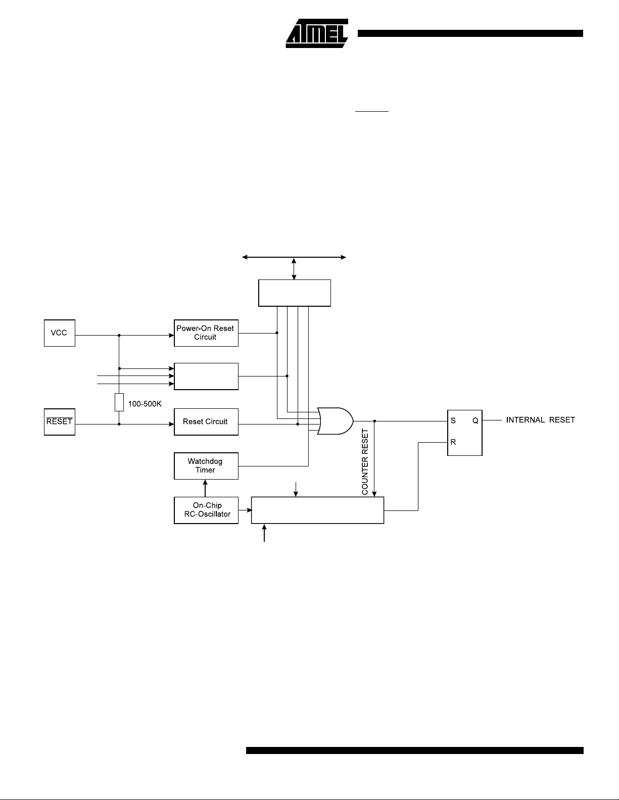
The ATmega161 has four sources of reset:
• Power-on Reset. The MCU is reset when the supply voltage is below the power-on reset threshold (V
POT
).
• External Reset. The MCU is reset when a low level is present on the RESET pin for more than 500 ns.
• Watchdog Reset. The MCU is reset when the Watchdog timer period expires and the Watchdog is enabled.
• Brown-out Reset. The MCU is reset when the supply voltage V
falls below a certain voltage.
CC
During reset, all I/O regist ers are the n set to their ini tial valu es, and the pro gram starts execution from address $000. The
instruction placed in address $000 must be an JMP – relative jump – instruction to the reset handling routine. If the program
never enables an interrupt source, the interrupt vectors are not used, and regular program code can be placed at thes e
locations. The cir cuit diagram in Figure 24 shows the reset logic. Ta ble 3 and Table 4 define s the timing and elec trical
parameters of the reset circuitry
Figure 24. Reset Logic
DATA BUS
MCU Status
Register (MCUSR)
BORF
WDRF
PORF
EXTRF
BODEN
BODLEVEL
Brown-Out
Reset Circuit
CK
CKSEL[2:0]
Delay Counters
Full
24
ATmega161(L)
ATmega161(L)
Table 3. Reset Characteristics (V
= 5.0V)
CC
Symbol Parameter Condition Min Typ Max Units
BOD disabled 1.0 1.4 1.8 V
Power-on Reset Threshold Voltage (rising)
BOD enabled 1.7 2.2 2.7 V
V
POT
BOD disabled 0.4 0.6 0.8 V
Power-on Reset Threshold Voltage (falling)
BOD enabled 1.7 2.2 2.7 V
V
RST
RESET Pin Threshold Voltage - - 0.85 V
CC
(BODLEVEL = 1) 2.6 2.7 2.8
V
BOT
Note: The Power-on Reset will not work unless the supply voltage has been below V
‘
Table 4. Reset Delay Selections
CKSEL
[2:0]
Brown-out R eset Threshold Voltage
Start-up Time, VCC = 2.7V,
BODLEVEL Unprogrammed
(BODLEVEL = 0) 3.8 4.0 4.2
(falling).
POT
Start-up Time, VCC = 4.0V,
BODLEVEL Programmed Recommended Usage
(1)
000 4.2 ms + 6 CK 5.8 ms + 6 CK External Clock, fast rising power
001 30 µs + 6 CK 10 µs + 6 CK External Clock, BOD enabled
(2)(3)
010 67 ms + 16K CK 92 ms + 16K CK Crystal Oscillator, slowly rising power
011 4.2 ms + 16K CK 5.8 ms + 16K CK Crystal Oscillator, fast rising power
100 30 µs + 16K CK 10 µs + 16K CK Crystal Oscillator, BOD enabled
(2)(3)
101 67 ms + 1K CK 92 ms + 1K CK Ceramic Resonator/External clock, Slowly rising power
V
V
110 4.2 ms + 1K CK 5.8 ms + 1K CK Ceramic Resonator, fast rising power
111 30 µs + 1K CK 10 µs + 1K CK Ceramic Resonator, BOD enabled
(2)(3)
Notes: 1. Th e CKSEL fuses con trol only the start-up ti me. The os cillator is the same fo r all sele ctions. On powe r-up, the rea l-ti me part
of the start-up time is increased with typ. 0.6ms.
2. Or external power-on reset.
3. When BOD is enabled, there will be a real-time part = 50 µs (typ.)
Table 4 shows th e start-up time s from reset . From slee p, only the clo ck counting part of the sta rt-up time is used. The
watchdog oscillator is used for timing the real-time part of the start-up time. The number WDT oscillator cycles used for
each time-out is shown in Table 5.
Table 5. Number of Watchdog Oscillator Cycles
BODLEVEL Time-out Number of cycles
Unprogrammed 4.2 ms (at Vcc=2.7V) 1K
Unprogrammed 67 ms (at V
Programmed 5.8 ms (at V
=2.7V) 16K
cc
=4.0V) 4K
cc
Programmed 92 ms (at Vcc=4.0V) 64K
Note: The bod-level fus e ca n b e u se d to s elect start-up times even if the Brown-o ut det ection is disabled (by le av ing th e BO DE N fuse
unprogrammed).
The frequency of the watchdog oscillator is voltage dependent as shown in the Electrical Characteristics section. The
device is shipped with CKSEL = 010.
25

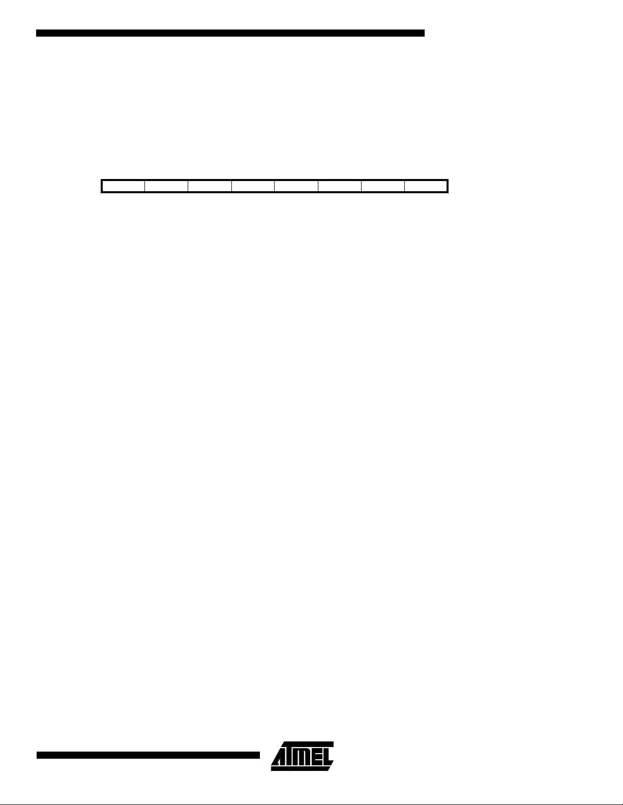
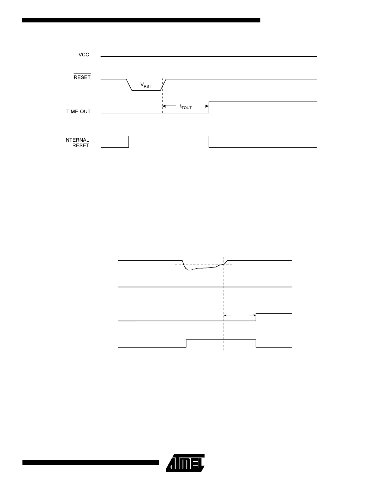
Power-on Reset
A Power-on Reset (POR) pulse is generated by an on-chip detection circuit. The detection level is nominally 1.4V (rising
VCC). The POR is activated whenever V
is below the detection level. The POR circuit can be used to trigger the start-up
CC
reset, as well as detect a failure in supply voltage.
A Power-on Reset (POR) circuit ensures that the device is reset from power-on. Reaching the power-on reset threshold
voltage invokes a delay cou nter, which determi nes the delay, for which the devi ce is kept in RE SET after V
rise. The
CC
time-out period of the delay counter can be defined by the user through the CKSEL fuses. The eight different selections for
the delay period are presented in Table 4. The RESET signal is activated again, without any delay, when the V
CC
decreases below detection level.
Figure 25. MCU Start-up, RESET
VCC
RESET
TIME-OUT
INTERNAL
RESET
Figure 26. MCU Start-up, RESET
VCC
RESET
TIME-OUT
Tied to VCC.
V
POT
V
RST
t
TOUT
Controlled Externally
V
POT
V
RST
t
TOUT
INTERNAL
RESET
External Reset
An external reset is generated by a l ow level on the RESET
pin. Reset pulses longer than 500 ns will generate a reset,
even if the clock is not running. Shorter pulses are not guaranteed to generate a reset. When the applied signal reaches the
Reset Threshold Voltage – V
on its positive edge, the delay timer starts the MCU after the Time-out period t
RST
TOUT
has
expired.
26
ATmega161(L)
ATmega161(L)
Figure 27. External Reset During Operation
Brown-out Detection
ATmega161 has an o n-chip brown -out dete ction (BOD) circuit for m onitori ng the V
circuit can be enabled/disabled by the fuse BODEN. When BODEN is enabled (BODEN programmed), and V
to a value bel ow t he t rigg er le vel , the b row n-ou t re set is i mmedi ate ly ac tiva te d. Wh en V
the brown-out reset is deactivated after a delay. The delay is defined by the user in the same way as the delay of POR signal, in Table 4. The trig ger level for the BOD can be sel ected by the fuse BODLEV EL to be 2.7V (BODLEVEL
unprogrammed), or 4.0V ((BODLEVEL programmed). The trigger level has a hysteresis of 50 mV to ensure spike free
brown-out detection.
The BOD circuit will only detect a drop in V
if the voltage stays below the trigger level for longer than 9 µs for trigger level
CC
4.0V, 21 µs for trig ger level 2.7V (typical values).
level during the operati on. T he BOD
CC
increases above the trigger level,
CC
decreases
CC
Figure 28. Brown-out Reset During Operation
VCC
RESET
TIME-OUT
INTERNAL
RESET
V
BOT-
V
BOT+
t
TOUT
Watchdog Reset
When the Watchdo g tim es out, it will genera te a sh ort rese t pulse o f 1 XT AL cyc le dur ation. On the fal ling edge of th is
pulse, the delay timer starts counting the Time-out period t
. Refer to Page page 52 for details on operation of the
TOUT
Watchdog.
27
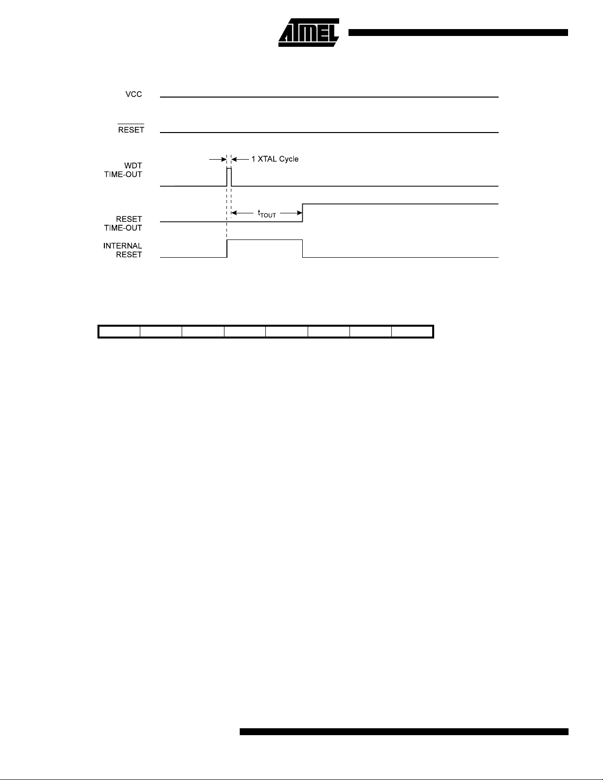
Figure 29. Watchdog Reset During Operation
MCU Status Register – MCUSR
The MCU Status Register provides information on which reset source caused an MCU reset.
Bit 76543210
$34 ($54) - - - - WDRF BORF EXTRF PORF MCUSR
Read/Write R R R R R/W R/W R/W R/W
Initial value 0 0 0 0 See bit description
Bits 7..4 - Res: Reserved Bits
•
These bits are reserved bits in the ATmega161 and always read as zero.
Bit 3 - WDRF: Watchdog Reset Flag
•
This bit is set if a watchdog reset occurs. The bit is cleared by a power-on reset, or by writing a logic zero to the flag.
•
Bit 2 - BORF: Brown-out Reset Flag
This bit is set if a brown-out reset occurs. The bit is cleared by a power-on reset, or by writing a logic zero to the flag.
Bit 1 - EXTRF: External Reset Flag
•
This bit is set if an external reset occurs. The bit is cleared by a power-on reset, or by writing a logic zero to the flag.
Bit 0 - PORF: Power-on Reset Flag
•
This bit is set if a power-on reset occurs. The bit is cleared only by writing a logic zero to the flag.
To make use of the reset flags to identify a reset condition, the user should read and then clear the MCUSR as early as
possible in the program. If th e regist er is clear ed before ano ther reset occurs, th e source of th e reset can be found by
examining the reset flags.
Interrupt Handling
The ATmega161 has two 8-bit Interrupt Mask control registe rs; GIMSK – Genera l Interrupt Ma sk register and TIM SK –
Timer/Counter Interrupt Mask register.
When an interrupt occurs, the Global Interrupt Enable I-bit is cleared (zero) and all interrupts are disabled. The user software can set (one) the I-bit to enabl e nested interrupts. The I-bit is set (one) when a Return from Interrupt instruction –
RETI – is executed.
When the Program Counter is vectored to the actual interrupt vector in order to execute the interrupt handling routine, hardware clears the corresponding flag that generated the interrupt. Some of the interrupt flags can also be cleared by writing a
logic one to the flag bit position(s) to be cleared.
If an interrupt condition occurs when the corresponding interrupt enable bit is cleared (zero), the interrupt flag will be set
and remembered until the interrupt is enabled, or the flag is cleared by software.
28
ATmega161(L)
ATmega161(L)
If one or more interrupt condi tions occu r when the global interrupt ena ble bit is clea red (zero), th e correspondi ng interrup t
flag(s) will be set and remembered until the global interrupt enable bit is set (one), and will be executed by order of priority.
Note that external level interrupt does not have a flag, and will only be remembered for as long as the interrupt condition is
present.
Note that the status register is not automatically stored when entering an interrupt routine and restored when returning from
an interrupt routine. This must be handled by software.
Interrupt Response Time
The interrupt execut ion respons e for all th e enabled A VR in terrupts is 4 clock cycles mi nimum. Afte r 4 clock cycles th e
program vec tor addre ss for the actual interru pt handl ing ro utine is execute d. Duri ng this 4 cl ock cyc le perio d, the Pr ogra m
Counter (13 bits) is pushed onto the Stack. The vector is normally a jump to the interrupt routine, and this jump takes
3 clock cycles. If an interrupt occurs during execution of a multi-cycle instruction, this instruction is completed before the
interrupt is served. If an interrupt occurs when the MCU is in sleep mode, the interrupt execution response time is
increased by 4 clock cycles.
A return from an interrupt handling routine takes 4 clock cycles. During these 4 clock cycles, the Program Counter (2 bytes)
is popped back from th e St ack , th e St ac k P oi nter is i nc remented by 2, and the I flag in S R E G is set. When AVR exits from
an interrupt, it wi ll always return to the main progr am and ex ecute one more in struction before a ny pendi ng interr upt is
served.
General Interrupt Mask Register – GIMSK
Bit 7 6 5 4 3 2 1 0
$3B ($5B) INT1 INT0 INT2 - - - - - GIMSK
Read/Write R/W R/W R R R R R R
Initial value 0 0 0 0 0 0 0 0
Bit 7 - INT1: External Interrupt Request 1 Enable
•
When the INT1 bit is set (one) and the I-bit in the Status Register (SREG) is set (one), the external pin interrupt is enabled.
The Interrupt Sense Control1 bits 1/0 (ISC11 and ISC10) in the MCU general Control Register (MCUCR) define whether
the external interrupt is ac tivated on rising and/or falli ng edge of the INT1 pin or level sense d. Acti vi ty on the pin will ca use
an interrupt request ev en if INT 1 i s co nfi gur ed as an output. The corresponding interrupt of Exte r nal Inte rrup t Re ques t 1 is
executed from program memory address $004. See also “External Interrupts”.
Bit 6 - INT0: External Interrupt Request 0 Enable
•
When the INT0 bit is set (one) and the I-bit in the Status Register (SREG) is set (one), the external pin interrupt is enabled.
The Interrupt Sense Control0 bits 1/0 (ISC01 and ISC00) in the MCU general Control Register (MCUCR) defines whet her
the external interrupt is ac tivated on rising and/or falli ng edge of the INT0 pin or level sense d. Acti vi ty on the pin will ca use
an interrupt request ev en if INT 0 i s co nfi gur ed as an output. The corresponding interrupt of Exte r nal Inte rrup t Re ques t 0 is
executed from program memory address $002. See also “External Interrupts.”
Bit 5- INT2: External Interrupt Request 2 Enable
•
When the INT2 bit is set (one) and the I-bit in the Status Register (SREG) is set (one), the external pin interrupt is activated.
The Interrupt Sense Control2 bit (ISC02 in the Extended MCU Control Register (EMCUCR) defines whether the external
interrupt is activated on rising or falling edge of the INT2 pin. Activity on the pin will cause an interrupt request even if INT2
is configured as an outp ut. The co rrespo nding inter rupt of Externa l Interru pt Reques t 2 is execute d from program m emory
address $006. See also “External Interrupts.”
Bits 4..0 - Res: Reserved bits
•
These bits are reserved bits in the ATmega161 and always read as zero.
29
General Interrupt Flag Register – GIFR
Bit 7 6 5 4 3 2 1 0
$3A ($5A) INTF1 INTF0 INTF2 - - - - - GIFR
Read/Write R/W R/W R/W R R R R R
Initial value 0 0 0 0 0 0 0 0
Bit 7 - INTF1: External Interrupt Flag1
•
When an event on the INT1 pin triggers an interrupt request, INTF1 becomes set (one). If the I-bit in SREG and the INT1 bit
in GIMSK are set (one), the MCU will jump to the interrupt vector at address $004. The flag is cleared when the interrupt
routine is executed. Alternatively, the flag can be cleared by writing a logical one to it.
Bit 6 - INTF0: External Interrupt Flag0
•
When an event on the INT0 pin triggers an interrupt request, INTF0 becomes set (one). If the I-bit in SREG and the INT0 bit
in GIMSK are set (one), the MCU will jump to the interrupt vector at address $002. The flag is cleared when the interrupt
routine is executed. Alternatively, the flag can be cleared by writing a logical one to it.
Bit 5 - INTF2: External Interrupt Flag2
•
When an event on the INT2 pin triggers an interrupt request, INTF2 becomes set (one). If the I-bit in SREG and the INT2 bit
in GIMSK are set (one), the MCU will jump to the interrupt vector at address $006. The flag is cleared when the interrupt
routine is executed. Alternatively, the flag can be cleared by writing a logical one to it.
Bits 4..0 - Res: Reserved bits
•
These bits are reserved bits in the ATmega161 and always read as zero.
Timer/counter Interrupt Mask Register – TIMSK
Bit 7 6 5 4 3 2 1 0
$39 ($59) TOIE1 OCIE1A OCIE1B TOIE2 TICIE1 OCIE2 TOIE0 OCIE0 TIMSK
Read/Write R/W R/W R/W R/W R/W R/W R/W R/W
Initial value 0 0 0 0 0 0 0 0
Bit 7 - TOIE1: Timer/Counter1 Overflow Interrupt Enable
•
When the TOIE1 bit is set (one) and the I-bit in the Status Register is set (one), the Timer/Counter1 Overflow interrupt is
enabled. The corresponding interrupt (at vector $012) is executed if an overflow in Timer/Counter1 occurs, i.e., when the
TOV1 bit is set in the Timer/Counter Interrupt Flag Register – TIFR.
Bit 6 - OCE1A:Timer/Counter1 Output CompareA Match Interrupt Enable
•
When the OCIE1A bit is set (one) and the I-bit in the Status Register is set (one), the Timer/Counter1 CompareA Match
interrupt is enabled. The corresponding interrupt (at vector $00e) is executed if a CompareA match in Timer/Counter1
occurs, i.e., when the OCF1A bit is set in the Timer/Counter Interrupt Flag Register – TIFR.
Bit 5 - OCIE1B:Timer/Counter1 Output CompareB Match Interrupt Enable
•
When the OCIE1B bit is set (one) and the I-bit in the Status Register is set (one), the Timer/Counter1 CompareB Match
interrupt is enabled. The corresponding interrupt (at vector $010) is executed if a CompareB match in Timer/Counter1
occurs, i.e., when the OCF1B bit is set in the Timer/Counter Interrupt Flag Register – TIFR.
Bit 4 - TOIE2: Timer/Counter2 Overflow Interrupt Enable
•
When the TOIE2 bit is set (one) and the I-bit in the Status Register is set (one), the Timer/Counter2 Overflow interrupt is
enabled. The corresponding interrupt (at vector $00a) is executed if an overflow in Timer/Counter2 occurs, i.e., when the
TOV2 bit is set in the Timer/Counter Interrupt Flag Register – TIFR.
Bit 3 - TICIE1: Timer/Counter1 Input Capture Interrupt Enable
•
When the TICIE1 bi t is set (o ne) and the I- bit in the Status Re gister is set (one), th e Time r/Counter 1 Input Capture Ev ent
Interrupt is enabled. The corresponding interrupt (at vector $00C) is executed if a capture-triggering event occurs on pin 31,
ICP, i.e., when the ICF1 bit is set in the Timer/Counter Interrupt Flag Register – TIFR.
Bit 2 - OCIE2:Timer/Counter2 Output Compare Match Interrupt Enable
•
When the OCIE2 bit is set (one) and the I- bit in t he Status Reg is ter is s et (one ), th e Tim er /Cou nter2 Co mpa re Matc h inte rrupt is enabled. T he corre sponding interru pt (at vect or $008) is execu ted if a Comp are2 ma tch in Tim er/Cou nter2 occ urs,
i.e., when the OCF2 bit is set in the Timer/Counter Interrupt Flag Register – TIFR.
30
ATmega161(L)
Loading...