


ATMEL ATF16V8CZ-15JC, ATF16V8CZ-12XC, ATF16V8CZ-12SC, ATF16V8CZ-12PC, ATF16V8CZ-12JC Datasheet
...
Features
∙Industry Standard Architecture Emulates Many 20-Pin PALs®
Low Cost Easy-to-Use Software Tools
∙High Speed Electrically Erasable Programmable Logic Devices 12 ns Maximum Pin-to-Pin Delay
∙Low Power - 25 μA Standby Power
∙CMOS and TTL Compatible Inputs and Outputs
∙Advanced Flash Technology Reprogrammable
100% Tested
∙High Reliability CMOS Process 20 Year Data Retention
100 Erase/Write Cycles
2,000V ESD Protection
200 mA Latchup Immunity
∙Commercial and Industrial Temperature Ranges
∙Dual Inline and Surface Mount Packages in Standard PinoutsInput and I/O Pin Keeper Circuits
Block Diagram
Pin Configurations
|
Pin Name |
Function |
|
|
CLK |
Clock |
|
|
|
|
|
|
I |
Logic Inputs |
|
|
|
|
|
|
I/O |
Bidirectional Buffers |
|
|
|
|
|
|
OE |
Output Enable |
|
|
VCC |
+5V Supply |
|
|
|
|
|
TSSOP Top View
I/CLK |
|
1 |
|
|
|
|
|
|
20 |
|
VCC |
||||
|
|
||||||
|
|
||||||
I1 |
|
2 |
19 |
|
I/O |
||
I2 |
|
3 |
18 |
|
I/O |
||
I3 |
|
4 |
17 |
|
I/O |
||
I4 |
|
5 |
16 |
|
I/O |
||
I5 |
|
6 |
15 |
|
I/O |
||
I6 |
|
7 |
14 |
|
I/O |
||
I7 |
|
8 |
13 |
|
I/O |
||
I8 |
|
9 |
12 |
|
I/O |
||
GND |
|
10 |
|
|
|
|
|
|
11 |
|
I9/OE |
||||
|
|
|
|
|
|
|
|
|
|
|
|
|
|
|
|
|
DIP/SOIC |
|
|
I/CLK |
1 |
20 |
Vcc |
I1 |
2 |
19 |
I/O |
I2 |
3 |
18 |
I/O |
I3 |
4 |
17 |
I/O |
I4 |
5 |
16 |
I/O |
I5 |
6 |
15 |
I/O |
I6 |
7 |
14 |
I/O |
I7 |
8 |
13 |
I/O |
I8 |
9 |
12 |
I/O |
GND |
10 |
11 |
I9/OE |
PLCC
|
I/CLK Vcc |
|
|
I2 I1 |
I/O |
I3 |
|
1 |
|
I/O |
|
I4 |
|
I/O |
I5 |
6 |
16 I/O |
I6 |
|
I/O |
I7 |
|
I/O |
|
|
11 |
|
I8 |
I/O I/O |
|
GND |
I9/OE |
Top view
High
Performance
E2 PLD
ATF16V8CZ
Rev. 0453C/V16FZ-C–04/98

Description (Continued)
The ATF16V8CZ is a high performance EECMOS Programmable Logic Device which utilizes Atmel’s proven electrically erasable Flash memory technology. Speeds down to 12 ns and a 25 μA edge-sensing power down mode are offered. All speed ranges are specified over the full 5V ± 10% range for industrial temperature ranges; 5V
± 5% for commercial range 5-volt devices.
The ATF16V8CZ incorporates a superset of the generic architectures, which allows direct replacement of the 16R8 family and most 20-pin combinatorial PLDs. Eight outputs are each allocated eight product terms. Three different
Absolute Maximum Ratings*
...................Temperature Under Bias |
-40°C to +85°C |
Storage Temperature...................... |
-65°C to +150°C |
Voltage on Any Pin with |
-2.0V to +7.0V (1) |
Respect to Ground......................... |
|
Voltage on Input Pins |
|
with Respect to Ground |
-2.0V to +14.0V (1) |
During Programming.................... |
|
Programming Voltage with |
-2.0V to +14.0V (1) |
Respect to Ground....................... |
|
|
|
modes of operation, configured automatically with software, allow highly complex logic functions to be realized.
The ATF16V8CZ can significantly reduce total system power, thereby enhancing system reliability and reducing power supply costs. When all the inputs and internal nodes are not switching, supply current drops to less than 2 5 μA. This automatic power down feature allows for power savings in slow clock systems and asynchronous applications. Also, the pin keeper circuits eliminate the need for internal pull-up resistors along with their attendant power consumption.
*NOTICE: Stresses beyond those listed under “Absolute Maximum Ratings” may cause permanent damage to the device. This is a stress rating only and functional operation of the device at these or any other conditions beyond those indicated in the operational sections of this specification is not implied. Exposure to absolute maximum rating conditions for extended periods may affect device reliability.
Note:
1.Minimum voltage is -0.6V dc, which may undershoot to - 2.0V for pulses of less than 20 ns. Maximum output pin voltage is Vcc + 0.75V dc, which may overshoot to 7.0V for pulses of less than 20 ns.
DC and AC Operating Conditions
|
Commercial |
Industrial |
Operating Temperature (Case) |
0°C - 70°C |
-40°C - 85°C |
|
|
|
VCC Power Supply |
5V ± 5% |
5V ± 10% |
2 ATF16V8CZ 
 ATF16V8CZ
DC Characteristics
Symbol |
Parameter |
Condition |
|
Min |
Typ |
Max |
Units |
IIL |
Input or I/O Low |
0 ≤ VIN ≤ VIL(MAX) |
|
|
|
-10 |
μA |
Leakage Current |
|
|
|
||||
|
|
|
|
|
|
|
|
IIH |
Input or I/O High |
3.5 ≤ VIN ≤ VCC |
|
|
|
10 |
μA |
Leakage Current |
|
|
|
||||
|
|
|
|
|
|
|
|
ICC1 |
Power Supply Current |
15 MHz, VCC = MAX, |
Com. |
|
|
95 |
mA |
VIN = 0, VCC, Outputs |
Ind. |
|
|
105 |
mA |
||
|
|
Open |
|
|
|||
|
|
|
|
|
|
|
|
ICC (1) |
Power Supply Current, |
MHz, VCC = MAX, |
Com. |
|
5 |
25 |
μA |
VIN = 0, VCC, Outputs |
|
|
|
|
|
||
|
Standby Mode |
Open |
Ind. |
|
5 |
50 |
μA |
|
|
|
|
|
|
|
|
IOS |
Output Short Circuit |
VOUT = 0.5V; VCC= |
|
|
|
-150 |
mA |
Current |
5V; TA = 25°C |
|
|
|
|||
|
|
|
|
|
|
||
VIL |
Input Low Voltage |
MIN < VCC < MAX |
|
-0.5 |
|
0.8 |
V |
VIH |
Input High Voltage |
|
|
2.0 |
|
VCC + 1 |
V |
VOL |
Output Low Current |
VCC = MIN; All Outputs |
Com., Ind. |
|
|
0.5 |
V |
|
|
IOL = -16 mA |
|
|
|
|
|
VOH |
Output High Current |
VCC = MIN |
|
2.4 |
|
|
V |
IOL = -3.2 mA |
|
|
|
||||
|
|
|
|
|
|
|
|
IOL |
Output Low Current |
VCC = MIN |
Com. |
24 |
|
|
mA |
Ind. |
12 |
|
|
||||
|
|
|
|
|
|
||
|
|
|
|
|
|
|
|
IOH |
Output High Current |
VCC = MIN |
Com., Ind. |
4 |
|
|
mA |
Note: 1. All ICC parameters measured with outputs open. |
|
|
|
|
|
||
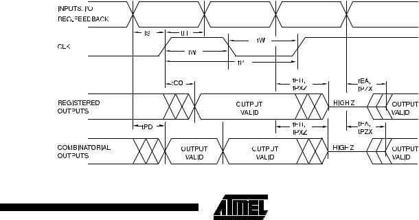
AC Waveforms (1)
Note: 1. Timing measurement reference is 1.5V. Input AC driving levels are 0.0V and 3.0V, unless otherwise specified.
3
 Loading...