


 Loading...
ATMEL AT90S2313-4SC, AT90S2313-4PI, AT90S2313-10SI, AT90S2313-10SC, AT90S2313-10PI Datasheet
...Features
•Utilizes the AVR® RISC Architecture
•AVR – High-performance and Low-power RISC Architecture
–118 Powerful Instructions – Most Single Clock Cycle Execution
–32 x 8 General-purpose Working Registers
–Up to 10 MIPS Throughput at 10 MHz
•Data and Nonvolatile Program Memory
–2K Bytes of In-System Programmable Flash
Endurance 1,000 Write/Erase Cycles
–128 Bytes of SRAM
–128 Bytes of In-System Programmable EEPROM Endurance: 100,000 Write/Erase Cycles
–Programming Lock for Flash Program and EEPROM Data Security
•Peripheral Features
–One 8-bit Timer/Counter with Separate Prescaler
–One 16-bit Timer/Counter with Separate Prescaler, Compare, Capture Modes and 8-, 9- or 10-bit PWM
–On-chip Analog Comparator
–Programmable Watchdog Timer with On-chip Oscillator
–SPI Serial Interface for In-System Programming
–Full Duplex UART
•• Special Microcontroller Features
–Low-power Idle and Power-down Modes
–External and Internal Interrupt Sources
•• Specifications
–Low-power, High-speed CMOS Process Technology
–Fully Static Operation
•Power Consumption at 4 MHz, 3V, 25°C
–Active: 2.8 mA
–Idle Mode: 0.8 mA
–Power-down Mode: <1 µA
•I/O and Packages
–15 Programmable I/O Lines
–20-pin PDIP and SOIC
•Operating Voltages
–2.7 - 6.0V (AT90S2313-4)
–4.0 - 6.0V (AT90S2313-10)
•Speed Grades
–0 - 4 MHz (AT90S2313-4)
–0 - 10 MHz (AT90S2313-10)
Pin Configuration
PDIP/SOIC
8-bit  Microcontroller with 2K Bytes of In-System Programmable Flash
AT90S2313
Rev. 0839G–08/01
1

Description
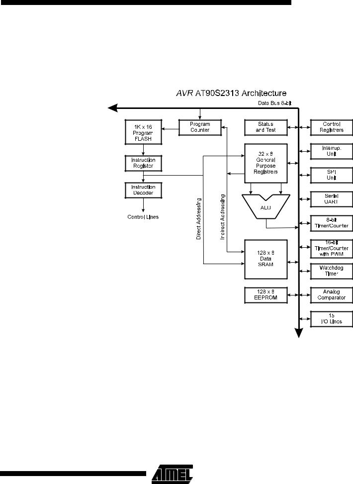
The AT90S2313 is a low-power CMOS 8-bit microcontroller based on the AVR RISC architecture. By executing powerful instructions in a single clock cycle, the AT90S2313 achieves throughputs approaching 1 MIPS per MHz allowing the system designer to optimize power consumption versus processing speed.
The AVR core combines a rich instruction set with 32 general-purpose working registers. All the 32 registers are directly connected to the Arithmetic Logic Unit (ALU), allowing two independent registers to be accessed in one single instruction executed in one clock cycle. The resulting architecture is more code efficient while achieving throughputs up to ten times faster than conventional CISC microcontrollers.
Figure 1. The AT90S2313 Block Diagram
The AT90S2313 provides the following features: 2K bytes of In-System Programmable Flash, 128 bytes EEPROM, 128 bytes SRAM, 15 general-purpose I/O lines, 32 generalpurpose working registers, flexible timer/counters with compare modes, internal and external interrupts, a programmable serial UART, programmable Watchdog Timer with internal oscillator, an SPI serial port for Flash memory downloading and two software
2 AT90S2313 
0839G–08/01

 AT90S2313
selectable power-saving modes. The Idle Mode stops the CPU while allowing the SRAM, timer/counters, SPI port and interrupt system to continue functioning. The Power-down Mode saves the register contents but freezes the oscillator, disabling all
|
|
|
other chip functions until the next external interrupt or hardware reset. |
|
|
|
The device is manufactured using Atmel’s high-density nonvolatile memory technology. |
|
|
|
The on-chip In-System Programmable Flash allows the program memory to be repro- |
|
|
|
grammed in-system through an SPI serial interface or by a conventional nonvolatile |
|
|
|
memory programmer. By combining an enhanced RISC 8-bit CPU with In-System Pro- |
|
|
|
grammable Flash on a monolithic chip, the Atmel AT90S2313 is a powerful |
|
|
|
microcontroller that provides a highly flexible and cost-effective solution to many embed- |
|
|
|
ded control applications. |
|
|
|
The AT90S2313 AVR is supported with a full suite of program and system development |
|
|
|
tools including: C compilers, macro assemblers, program debugger/simulators, in-circuit |
|
|
|
emulators and evaluation kits. |
Pin Descriptions |
|
||
VCC |
Supply voltage pin. |
||
GND |
Ground pin. |
||
Port B (PB7..PB0) |
Port B is an 8-bit bi-directional I/O port. Port pins can provide internal pull-up resistors |
||
|
|
|
(selected for each bit). PB0 and PB1 also serve as the positive input (AIN0) and the |
|
|
|
negative input (AIN1), respectively, of the on-chip analog comparator. The Port B output |
|
|
|
buffers can sink 20 mA and can drive LED displays directly. When pins PB0 to PB7 are |
|
|
|
used as inputs and are externally pulled low, they will source current if the internal pull- |
|
|
|
up resistors are activated. The Port B pins are tri-stated when a reset condition |
|
|
|
becomes active, even if the clock is not active. |
|
|
|
Port B also serves the functions of various special features of the AT90S2313 as listed |
|
|
|
on page 53. |
Port D (PD6..PD0) |
Port D has seven bi-directional I/O ports with internal pull-up resistors, PD6..PD0. The |
||
|
|
|
Port D output buffers can sink 20 mA. As inputs, Port D pins that are externally pulled |
|
|
|
low will source current if the pull-up resistors are activated. The Port D pins are tri-stated |
|
|
|
when a reset condition becomes active, even if the clock is not active. |
|
|
|
Port D also serves the functions of various special features of the AT90S2313 as listed |
|
|
|
on page 58. |
|
Reset input. A low level on this pin for more than 50 ns will generate a reset, even if the |
||
|
RESET |
|
|
|
|
|
clock is not running. Shorter pulses are not guaranteed to generate a reset. |
XTAL1 |
Input to the inverting oscillator amplifier and input to the internal clock operating circuit. |
||
XTAL2 |
Output from the inverting oscillator amplifier. |
||
3
0839G–08/01
Crystal Oscillator
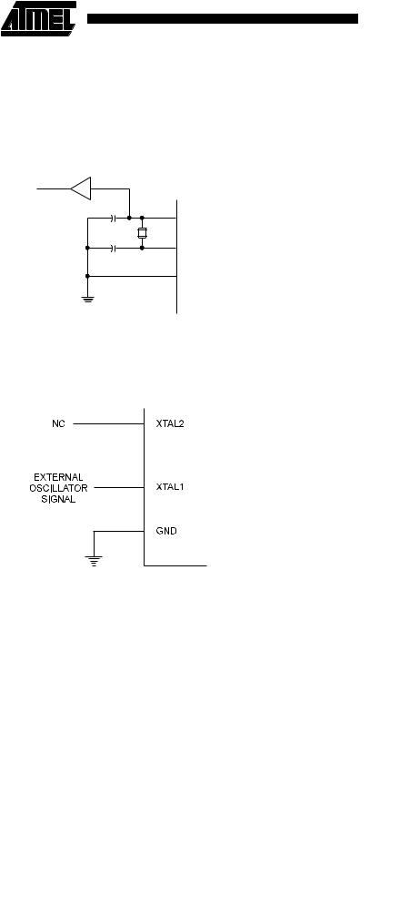
XTAL1 and XTAL2 are input and output, respectively, of an inverting amplifier that can be configured for use as an on-chip oscillator, as shown in Figure 2. Either a quartz crystal or a ceramic resonator may be used. To drive the device from an external clock source, XTAL2 should be left unconnected while XTAL1 is driven, as shown in Figure 3.
Figure 2. Oscillator Connections
MAX 1 HC BUFFER
HC
C2
XTAL2
C1
XTAL1
GND
Note: When using the MCU Oscillator as a clock for an external device, an HC buffer should be connected as indicated in the figure.
Figure 3. External Clock Drive Configuration
4 AT90S2313 
0839G–08/01
Architectural
Overview
AT90S2313
The fast-access register file concept contains 32 x 8-bit general-purpose working registers with a single clock cycle access time. This means that during one single clock cycle, one ALU (Arithmetic Logic Unit) operation is executed. Two operands are output from the register file, the operation is executed, and the result is stored back in the register file – in one clock cycle.
Figure 4. The AT90S2313 AVR RISC Architecture
Six of the 32 registers can be used as three 16-bit indirect address register pointers for Data Space addressing – enabling efficient address calculations. One of the three address pointers is also used as the address pointer for the constant table look-up function. These added function registers are the 16-bit X-register, Y-register and Z-register.
The ALU supports arithmetic and logic functions between registers or between a constant and a register. Single register operations are also executed in the ALU. Figure 4 shows the AT90S2313 AVR RISC microcontroller architecture.
In addition to the register operation, the conventional memory addressing modes can be used on the register file as well. This is enabled by the fact that the register file is assigned the 32 lowermost Data Space addresses ($00 - $1F), allowing them to be accessed as though they were ordinary memory locations.
5
0839G–08/01

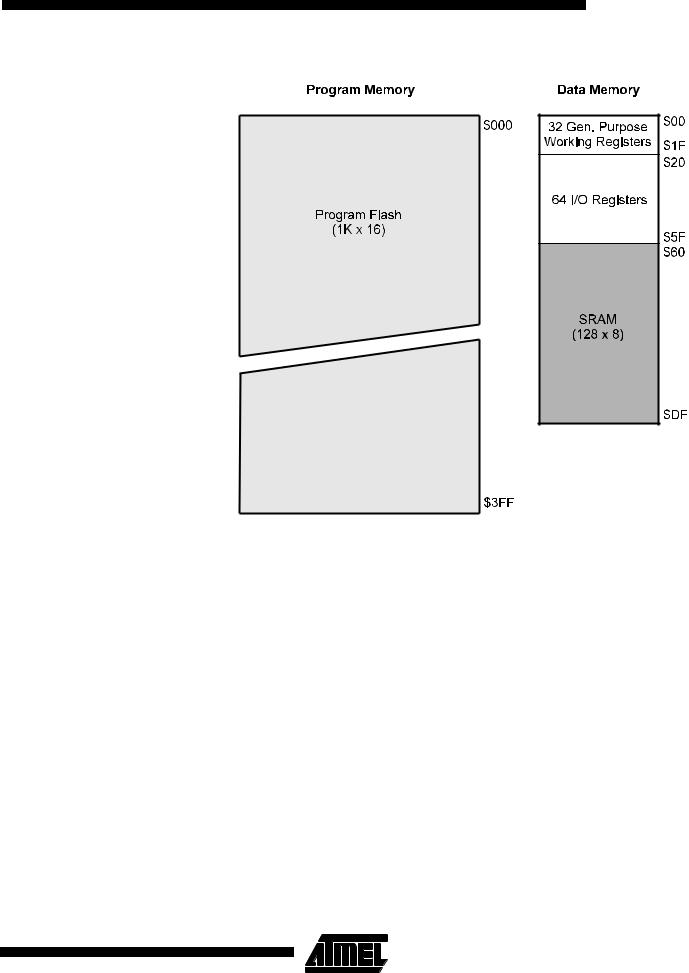
The I/O memory space contains 64 addresses for CPU peripheral functions such as control registers, timer/counters, A/D converters and other I/O functions. The I/O memory can be accessed directly or as the Data Space locations following those of the register file, $20 - $5F.
The AVR has Harvard architecture – with separate memories and buses for program and data. The program memory is accessed with a 2-stage pipeline. While one instruction is being executed, the next instruction is pre-fetched from the program memory. This concept enables instructions to be executed in every clock cycle. The program memory is In-System Programmable Flash memory.
With the relative jump and call instructions, the whole 1K address space is directly accessed. Most AVR instructions have a single 16-bit word format. Every program memory address contains a 16or 32-bit instruction.
During interrupts and subroutine calls, the return address Program Counter (PC) is stored on the stack. The stack is effectively allocated in the general data SRAM, and consequently the stack size is only limited by the total SRAM size and the usage of the SRAM. All user programs must initialize the SP in the reset routine (before subroutines or interrupts are executed). The 8-bit stack pointer (SP) is read/write accessible in the I/O space.
The 128 bytes data SRAM + register file and I/O registers can be easily accessed through the five different addressing modes supported in the AVR architecture.
The memory spaces in the AVR architecture are all linear and regular memory maps.
6 AT90S2313 
0839G–08/01
AT90S2313
Figure 5. Memory Maps
A flexible interrupt module has its control registers in the I/O space with an additional global interrupt enable bit in the Status Register. All the different interrupts have a separate interrupt vector in the interrupt vector table at the beginning of the program memory. The different interrupts have priority in accordance with their interrupt vector position. The lower the interrupt vector address, the higher the priority.
7
0839G–08/01

General-purpose
Register File
Figure 6 shows the structure of the 32 general-purpose registers in the CPU.
Figure 6. AVR CPU General-purpose Working Registers
7 |
0 |
Addr. |
|
||
|
|
|
R0 |
$00 |
|
|
|
|
|
$01 |
|
|
|
|
R1 |
|
|
|
|
|
|
$02 |
|
|
|
|
R2 |
|
|
|
|
|
|
|
|
|
|
|
… |
|
|
|
|
|
|
$0D |
|
|
|
|
R13 |
|
|
|
|
|
|
$0E |
|
General |
|
R14 |
|
||
|
|
|
|
$0F |
|
Purpose |
|
R15 |
|
||
|
|
|
|
|
|
Working |
|
|
R16 |
$10 |
|
|
|
|
|
$11 |
|
Registers |
|
R17 |
|
||
|
|
|
|
|
|
|
|
|
… |
|
|
|
|
|
|
$1A |
X-register low byte |
|
|
|
R26 |
||
|
|
|
|
$1B |
X-register high byte |
|
|
|
R27 |
||
|
|
|
|
$1C |
Y-register low byte |
|
|
|
R28 |
||
|
|
|
|
$1D |
Y-register high byte |
|
|
|
R29 |
||
|
|
|
|
$1E |
Z-register low byte |
|
|
|
R30 |
||
|
|
|
|
$1F |
Z-register high byte |
|
|
|
R31 |
||
|
|
|
|
|
|
All the register operating instructions in the instruction set have direct and single-cycle access to all registers. The only exception is the five constant arithmetic and logic instructions SBCI, SUBI, CPI, ANDI, ORI between a constant and a register and the LDI instruction for load immediate constant data. These instructions apply to the second half of the registers in the register file (R16..R31). The general SBC, SUB, CP, AND, OR and all other operations between two registers or on a single register apply to the entire register file.
As shown in Figure 6, each register is also assigned a data memory address, mapping them directly into the first 32 locations of the user Data Space. Although the register file is not physically implemented as SRAM locations, this memory organization provides great flexibility in access of the registers, as the X, Y and Z registers can be set to index any register in the file.
X-register, Y-register, and Z- The registers R26..R31 have some added functions to their general-purpose usage. register These registers are the address pointers for indirect addressing of the Data Space. The
three indirect address registers X, Y and Z are defined in Figure 7.
Figure 7. X, Y and Z Registers
|
15 |
|
|
|
|
0 |
X-register |
7 |
|
0 |
7 |
0 |
|
|
|
R27 ($1B) |
|
|
R26 ($1A) |
|
|
15 |
|
|
|
|
0 |
Y-register |
7 |
|
0 |
|
7 |
0 |
|
|
R29 |
($1D) |
|
|
R28 ($1C) |
|
15 |
|
|
|
|
0 |
Z-register |
7 |
|
0 |
|
7 |
0 |
|
|
R31 |
($1F) |
|
|
R30 ($1E) |
8 AT90S2313 
0839G–08/01

ALU – Arithmetic Logic
Unit
In-System
Programmable Flash
Program Memory
EEPROM Data Memory
AT90S2313
In the different addressing modes these address registers have functions as fixed displacement, automatic increment and decrement (see the descriptions for the different instructions).
The high-performance AVR ALU operates in direct connection with all the 32 generalpurpose working registers. Within a single clock cycle, ALU operations between registers in the register file are executed. The ALU operations are divided into three main categories – arithmetic, logical and bit functions.
The AT90S2313 contains 2K bytes on-chip In-System Programmable Flash memory for program storage. Since all instructions are 16or 32-bit words, the Flash is organized as 1K x 16. The Flash memory has an endurance of at least 1,000 write/erase cycles.
The AT90S2313 Program Counter (PC) is 10 bits wide, thus addressing the 1,024 program memory addresses.
See page 62 for a detailed description on Flash data downloading. See page 11 for the different addressing modes.
The AT90S2313 contains 128 bytes of EEPROM data memory. It is organized as a separate data space in which single bytes can be read and written. The EEPROM has an endurance of at least 100,000 write/erase cycles. The access between the EEPROM and the CPU is described on page 40, specifying the EEPROM address register, the EEPROM data register and the EEPROM control register.
For the SPI data downloading, see page 69 for a detailed description.
9
0839G–08/01

SRAM Data Memory
Figure 8 shows how the AT90S2313 data memory is organized.
Figure 8. SRAM Organization
Register File |
Data Address Space |
|
R0 |
|
$00 |
R1 |
|
$01 |
R2 |
|
$02 |
… |
|
… |
|
|
|
R29 |
|
$1D |
R30 |
|
$1E |
R31 |
|
$1F |
I/O Registers |
|
|
$00 |
|
$20 |
$01 |
|
$21 |
$02 |
|
$22 |
… |
|
… |
|
|
|
$3D |
|
$5D |
$3E |
|
$5E |
$3F |
|
$5F |
|
|
Internal SRAM |
|
|
$60 |
|
|
$61 |
|
|
$62 |
|
|
… |
|
|
|
|
|
$DD |
|
|
$DE |
|
|
$DF |
The 224 data memory locations address the Register file, I/O memory and the data SRAM. The first 96 locations address the Register File + I/O Memory, and the next 128 locations address the data SRAM.
The five different addressing modes for the data memory cover: Direct, Indirect with Displacement, Indirect, Indirect with Pre-decrement and Indirect with Post-increment. In the register file, registers R26 to R31 feature the indirect addressing pointer registers.
The Direct addressing reaches the entire data address space.
The Indirect with Displacement mode features 63 address locations reached from the base address given by the Y and Z registers.
When using register indirect addressing modes with automatic pre-decrement and postincrement, the address registers X, Y and Z are used and decremented and incremented.
The 32 general-purpose working registers, 64 I/O registers and the 128 bytes of data SRAM in the AT90S2313 are all directly accessible through all these addressing modes.
10 AT90S2313 
0839G–08/01
Program and Data
Addressing Modes
Register Direct, Single
Register Rd
AT90S2313
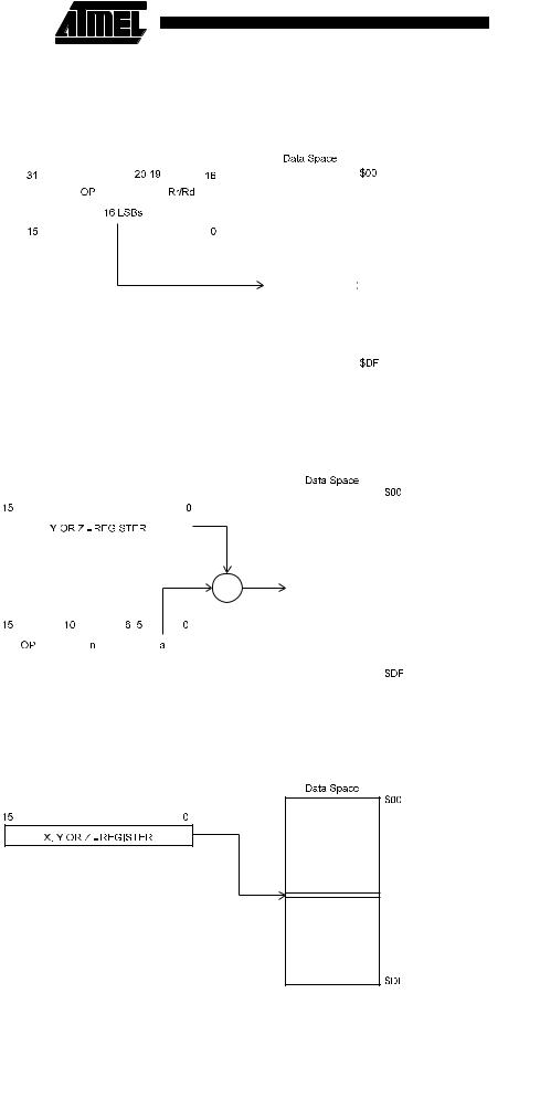
The AT90S2313 AVR RISC microcontroller supports powerful and efficient addressing modes for access to the program memory (Flash) and data memory. This section describes the different addressing modes supported by the AVR architecture. In the figures, OP means the operation code part of the instruction word. To simplify, not all figures show the exact location of the addressing bits.
Figure 9. Direct Single Register Addressing
|
The operand is contained in register d (Rd). |
|||||||
Register Direct, Two |
Figure 10. Direct Register Addressing, Two Registers |
|||||||
Registers Rd and Rr |
|
|
|
|
|
|
|
|
|
|
|
|
|
|
|
|
|
|
|
|
|
|
|
|
|
|
|
|
|
|
|
|
|
|
|
|
|
|
|
|
|
|
|
|
|
|
|
|
|
|
|
|
|
|
|
|
|
|
|
|
|
|
|
|
|
|
|
|
|
|
|
|
|
|
|
|
|
|
|
|
|
|
|
|
|
|
|
|
|
|
Operands are contained in register r (Rr) and d (Rd). The result is stored in register d |
|||||||
|
(Rd). |
|||||||
I/O Direct |
Figure 11. I/O Direct Addressing |
|||||||
|
|
|
|
|
|
|
|
|
|
|
|
|
|
|
|
|
|
|
|
|
|
|
|
|
|
|
|
|
|
|
|
|
|
|
|
|
|
|
|
|
|
|
|
|
|
|
|
|
|
|
|
|
|
|
|
|
|
|
|
|
|
|
|
|
|
|
|
|
|
|
|
11
0839G–08/01
|
Operand address is contained in 6 bits of the instruction word. n is the destination or |
|
source register address. |
Data Direct |
Figure 12. Direct Data Addressing |
|
|
|
|
|
|
|
|
|
|
|
|
|
|
|
|
|
|
|
|
|
|
|
|
|
|
|
|
|
|
|
|
|
|
|
|
|
|
|
|
|
|
|
|
|
|
|
|
|
|
|
|
|
|
|
|
|
|
|
|
|
|
|
|
|
|
|
|
|
|
|
|
|
|
|
|
|
|
|
|
|
|
|
|
|
|
|
|
|
|
|
|
|
|
|
|
|
|
|
|
|
|
|
|
|
|
|
|
|
A 16-bit data address is contained in the 16 LSBs of a 2-word instruction. Rd/Rr specify |
||||||||||||||||
|
the destination or source register. |
||||||||||||||||
Data Indirect with |
Figure 13. Data Indirect with Displacement |
||||||||||||||||
Displacement |
|
|
|
|
|
|
|
|
|
|
|
|
|
|
|
|
|
|
|
|
|
|
|
|
|
|
|
|
|
|
|
|
|
|
|
|
|
|
|
|
|
|
|
|
|
|
|
|
|
|
|
|
|
|
|
|
|
|
|
|
|
|
|
|
|
|
|
|
|
|
|
|
|
|
|
|
|
|
|
|
|
|
|
|
|
|
|
|
|
|
|
|
|
|
|
|
|
|
|
|
|
|
|
|
|
|
|
|
|
|
|
|
|
|
|
|
|
|
|
|
|
|
|
|
|
|
|
|
|
|
|
|
|
|
|
|
|
|
|
|
|
|
|
|
|
|
|
|
|
|
|
|
|
|
|
|
|
|
|
|
|
|
|
|
|
|
|
|
|
|
|
|
|
|
|
|
|
|
|
|
Operand address is the result of the Y- or Z-register contents added to the address con- |
|
tained in 6 bits of the instruction word. |
Data Indirect |
Figure 14. Data Indirect Addressing |
Operand address is the contents of the X-, Y- or Z-register.
12 AT90S2313 
0839G–08/01
AT90S2313
Data Indirect with Pre- |
Figure 15. Data Indirect Addressing with Pre-decrement |
|||||||
decrement |
|
|
|
|
|
|
|
|
|
|
|
|
|
|
|
|
|
|
|
|
|
|
|
|
|
|
|
|
|
|
|
|
|
|
|
|
|
|
|
|
|
|
|
|
|
|
|
|
|
|
|
|
|
|
|
|
|
|
|
|
|
|
|
|
|
|
|
|
|
|
|
|
|
|
|
|
|
|
|
|
|
|
|
|
|
|
|
|
|
|
The X-, Y- or Z-register is decremented before the operation. Operand address is the |
||||||||||
|
decremented contents of the X-, Y- or Z-register. |
||||||||||
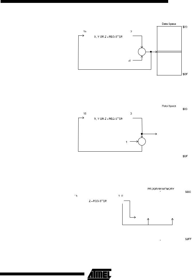
Data Indirect with Post- |
Figure 16. Data Indirect Addressing with Post-increment |
||||||||||
increment |
|
|
|
|
|
|
|
|
|
|
|
|
|
|
|
|
|
|
|
|
|
|
|
|
|
|
|
|
|
|
|
|
|
|
|
|
|
|
|
|
|
|
|
|
|
|
|
|
|
|
|
|
|
|
|
|
|
|
|
|
|
|
|
|
|
|
|
|
|
|
|
|
|
|
|
|
|
|
|
|
|
|
|
|
|
|
|
|
|
|
|
|
|
|
|
|
|
|
|
|
|
|
|
|
|
|
|
|
|
|
|
|
|
|
|
|
|
|
|
|
|
|
|
|
|
|
|
|
|
|
|
|
|
|
|
|
|
|
|
|
|
|
|
|
|
|
|
|
|
|
|
|
|
|
|
|
The X-, Y- or Z-register is incremented after the operation. Operand address is the con- |
|||||||
|
tents of the X-, Y- or Z-register prior to incrementing. |
|||||||
Constant Addressing Using |
Figure 17. Code Memory Constant Addressing |
|||||||
the LPM Instruction |
|
|
|
|
|
|
|
|
|
|
|
|
|
|
|
|
|
|
|
|
|
|
|
|
|
|
|
|
|
|
|
|
|
|
|
|
|
|
|
|
|
|
|
|
|
|
|
|
|
|
|
|
|
|
|
|
|
|
|
|
|
|
|
|
|
|
|
|
|
|
|
|
|
|
|
|
|
|
|
|
Constant byte address is specified by the Z-register contents. The 15 MSBs select word address (0 - 1K), the LSB selects low byte if cleared (LSB = 0) or high byte if set (LSB = 1).
13
0839G–08/01
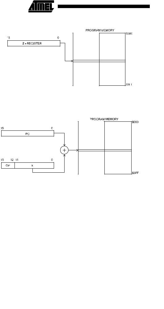
Indirect Program Addressing, Figure 18. Indirect Program Memory Addressing
IJMP and ICALL
Program execution continues at address contained by the Z-register (i.e., the PC is loaded with the contents of the Z-register).
Relative Program Addressing, Figure 19. Relative Program Memory Addressing
RJMP and RCALL
Memory Access and
Instruction Execution
Timing
Program execution continues at address PC + k + 1. The relative address k is -2048 to 2047.
This section describes the general access timing concepts for instruction execution and internal memory access.
The AVR CPU is driven by the System Clock Ø, directly generated from the external clock crystal for the chip. No internal clock division is used.
Figure 20 shows the parallel instruction fetches and instruction executions enabled by the Harvard architecture and the fast-access register file concept. This is the basic pipelining concept to obtain up to 1 MIPS per MHz with the corresponding unique results for functions per cost, functions per clocks and functions per power-unit.
14 AT90S2313 
0839G–08/01
AT90S2313
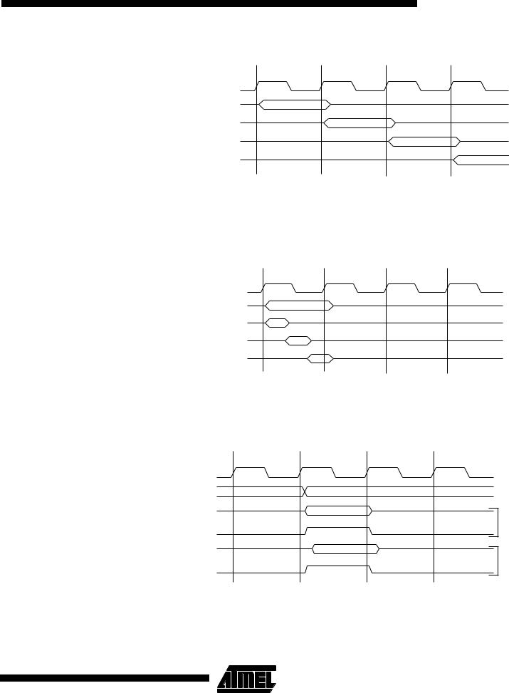
Figure 20. The Parallel Instruction Fetches and Instruction Executions
T1 |
T2 |
T3 |
T4 |
System Clock Ø
1st Instruction Fetch
1st Instruction Execute 2nd Instruction Fetch 2nd Instruction Execute 3rd Instruction Fetch 3rd Instruction Execute 4th Instruction Fetch
Figure 21 shows the internal timing concept for the register file. In a single clock cycle an ALU operation using two register operands is executed, and the result is stored back to the destination register.
Figure 21. Single-cycle ALU Operation
T1 |
T2 |
T3 |
T4 |
System Clock Ø
Total Execution Time
Register Operands Fetch
ALU Operation Execute
Result Write Back
The internal data SRAM access is performed in two System Clock cycles as described in Figure 22.
Figure 22. On-chip Data SRAM Access Cycles
T1 |
T2 |
T3 |
T4 |
System Clock Ø
Address |
Prev. Address |
Address |
Data
WR
Data
RD
Read Write
15
0839G–08/01

I/O Memory
The I/O space definition of the AT90S2313 is shown in Table 1.
Table 1. |
AT90S2313 I/O Space |
|
|
Address Hex |
Name |
Function |
|
|
|
|
|
$3F |
($5F) |
SREG |
Status Register |
|
|
|
|
$3D |
($5D) |
SPL |
Stack Pointer Low |
|
|
|
|
$3B |
($5B) |
GIMSK |
General Interrupt MaSK register |
|
|
|
|
$3A |
($5A) |
GIFR |
General Interrupt Flag Register |
|
|
|
|
$39 |
($59) |
TIMSK |
Timer/Counter Interrupt MaSK register |
|
|
|
|
$38 |
($58) |
TIFR |
Timer/Counter Interrupt Flag register |
|
|
|
|
$35 |
($55) |
MCUCR |
MCU general Control Register |
|
|
|
|
$33 |
($53) |
TCCR0 |
Timer/Counter 0 Control Register |
|
|
|
|
$32 |
($52) |
TCNT0 |
Timer/Counter 0 (8-bit) |
|
|
|
|
$2F |
($4F) |
TCCR1A |
Timer/Counter 1 Control Register A |
|
|
|
|
$2E |
($4E) |
TCCR1B |
Timer/Counter 1 Control Register B |
|
|
|
|
$2D |
($4D) |
TCNT1H |
Timer/Counter 1 High Byte |
|
|
|
|
$2C |
($4C) |
TCNT1L |
Timer/Counter 1 Low Byte |
|
|
|
|
$2B |
($4B) |
OCR1AH |
Output Compare Register 1 High Byte |
|
|
|
|
$2A |
($4A) |
OCR1AL |
Output Compare Register 1 Low Byte |
|
|
|
|
$25 |
($45) |
ICR1H |
T/C 1 Input Capture Register High Byte |
|
|
|
|
$24 |
($44) |
ICR1L |
T/C 1 Input Capture Register Low Byte |
|
|
|
|
$21 |
($41) |
WDTCR |
Watchdog Timer Control Register |
|
|
|
|
$1E |
($3E) |
EEAR |
EEPROM Address Register |
|
|
|
|
$1D |
($3D) |
EEDR |
EEPROM Data Register |
|
|
|
|
$1C |
($3C) |
EECR |
EEPROM Control Register |
|
|
|
|
$18 |
($38) |
PORTB |
Data Register, Port B |
|
|
|
|
$17 |
($37) |
DDRB |
Data Direction Register, Port B |
|
|
|
|
$16 |
($36) |
PINB |
Input Pins, Port B |
|
|
|
|
$12 |
($32) |
PORTD |
Data Register, Port D |
|
|
|
|
$11 ($31) |
DDRD |
Data Direction Register, Port D |
|
|
|
|
|
$10 |
($30) |
PIND |
Input Pins, Port D |
|
|
|
|
$0C |
($2C) |
UDR |
UART I/O Data Register |
|
|
|
|
$0B |
($2B) |
USR |
UART Status Register |
|
|
|
|
$0A |
($2A) |
UCR |
UART Control Register |
|
|
|
|
$09 |
($29) |
UBRR |
UART Baud Rate Register |
|
|
|
|
$08 |
($28) |
ACSR |
Analog Comparator Control and Status Register |
|
|
|
|
Note: Reserved and unused locations are not shown in the table.
All AT90S2313 I/O and peripherals are placed in the I/O space. The I/O locations are accessed by the IN and OUT instructions transferring data between the 32 general-pur-
16 AT90S2313 
0839G–08/01

 AT90S2313
pose working registers and the I/O space. I/O registers within the address range $00 - $1F are directly bit-accessible using the SBI and CBI instructions. In these registers, the value of single bits can be checked by using the SBIS and SBIC instructions. Refer to the instruction set section for more details. When using the I/O specific commands IN and OUT, the I/O addresses $00 - $3F must be used. When addressing I/O registers as SRAM, $20 must be added to this address. All I/O register addresses throughout this document are shown with the SRAM address in parentheses.
For compatibility with future devices, reserved bits should be written to zero if accessed. Reserved I/O memory addresses should never be written.
Some of the status flags are cleared by writing a logical “1” to them. Note that the CBI and SBI instructions will operate on all bits in the I/O register, writing a “1” back into any flag read as set, thus clearing the flag. The CBI and SBI instructions work with registers $00 to $1F only.
The I/O and peripherals control registers are explained in the following sections.
Status Register – SREG |
The AVR Status Register (SREG) at I/O space location $3F ($5F) is defined as: |
|
|||||||||
|
Bit |
7 |
6 |
5 |
4 |
3 |
2 |
1 |
0 |
|
|
|
$3F ($5F) |
|
|
|
|
|
|
|
|
|
SREG |
|
I |
T |
H |
S |
V |
N |
Z |
C |
|
||
|
Read/Write |
R/W |
R/W |
R/W |
R/W |
R/W |
R/W |
R/W |
R/W |
|
|
|
Initial value |
0 |
0 |
0 |
0 |
0 |
0 |
0 |
0 |
|
|
• Bit 7 – I: Global Interrupt Enable
The global interrupt enable bit must be set (one) for the interrupts to be enabled. The individual interrupt enable control is then performed in separate control registers. If the global interrupt enable bit is cleared (zero), none of the interrupts are enabled independent of the individual interrupt enable settings. The I-bit is cleared by hardware after an interrupt has occurred, and is set by the RETI instruction to enable subsequent interrupts.
• Bit 6 – T: Bit Copy Storage
The bit copy instructions BLD (Bit LoaD) and BST (Bit STore) use the T-bit as source and destination for the operated bit. A bit from a register in the register file can be copied into T by the BST instruction, and a bit in T can be copied into a bit in a register in the register file by the BLD instruction.
• Bit 5 – H: Half-carry Flag
The half-carry flag H indicates a half-carry in some arithmetic operations. See the Instruction Set description for detailed information.
• Bit 4 – S: Sign Bit, S = N V
The S-bit is always an exclusive or between the negative flag N and the two’s complement overflow flag V. See the Instruction Set description for detailed information.
• Bit 3 – V: Two’s Complement Overflow Flag
The two’s complement overflow flag V supports two’s complement arithmetics. See the Instruction Set description for detailed information.
• Bit 2 – N: Negative Flag
The negative flag N indicates a negative result after the different arithmetic and logic operations. See the Instruction Set description for detailed information.
• Bit 1 – Z: Zero Flag
The zero flag Z indicates a zero result after the different arithmetic and logic operations. See the Instruction Set description for detailed information.
17
0839G–08/01

Stack Pointer – SP
Reset and Interrupt
Handling
• Bit 0 – C: Carry Flag
The carry flag C indicates a carry in an arithmetic or logic operation. See the Instruction Set description for detailed information.
Note that the Status Register is not automatically stored when entering an interrupt routine and restored when returning from an interrupt routine. This must be handled by software.
An 8-bit register at I/O address $3D ($5D) forms the stack pointer of the AT90S2313. 8 bits are used to address the 128 bytes of SRAM in locations $60 - $DF.
Bit |
7 |
6 |
5 |
4 |
3 |
2 |
1 |
0 |
|
$3D ($5D) |
SP7 |
SP6 |
SP5 |
SP4 |
SP3 |
SP2 |
SP1 |
SP0 |
SPL |
Read/Write |
R/W |
R/W |
R/W |
R/W |
R/W |
R/W |
R/W |
R/W |
|
Initial value |
0 |
0 |
0 |
0 |
0 |
0 |
0 |
0 |
|
The Stack Pointer points to the data SRAM stack area where the Subroutine and Interrupt stacks are located. This stack space in the data SRAM must be defined by the program before any subroutine calls are executed or interrupts are enabled. The Stack Pointer must be set to point above $60. The Stack Pointer is decremented by 1 when data is pushed onto the stack with the PUSH instruction, and it is decremented by 2 when an address is pushed onto the stack with subroutine calls and interrupts. The Stack Pointer is incremented by 1 when data is popped from the stack with the POP instruction, and it is incremented by 2 when an address is popped from the stack with return from subroutine RET or return from interrupt RETI.
The AT90S2313 provides 10 different interrupt sources. These interrupts and the separate reset vector each have a separate program vector in the program memory space. All the interrupts are assigned individual enable bits that must be set (one) together with the I-bit in the Status Register in order to enable the interrupt.
The lowest addresses in the program memory space are automatically defined as the Reset and Interrupt vectors. The complete list of vectors is shown in Table 2. The list also determines the priority levels of the different interrupts. The lower the address, the higher the priority level. RESET has the highest priority, and next is INT0 (the External Interrupt Request 0), etc.
Table 2. Reset and Interrupt Vectors
Vector No. |
Program Address |
Source |
Interrupt Definition |
|
|
|
Hardware Pin, Power-on Reset and |
1 |
$000 |
RESET |
Watchdog Reset |
|
|
|
|
2 |
$001 |
INT0 |
External Interrupt Request 0 |
|
|
|
|
3 |
$002 |
INT1 |
External Interrupt Request 1 |
|
|
|
|
4 |
$003 |
TIMER1 CAPT1 |
Timer/Counter1 Capture Event |
|
|
|
|
5 |
$004 |
TIMER1 COMP1 |
Timer/Counter1 Compare Match |
|
|
|
|
6 |
$005 |
TIMER1 OVF1 |
Timer/Counter1 Overflow |
|
|
|
|
7 |
$006 |
TIMER0 OVF0 |
Timer/Counter0 Overflow |
|
|
|
|
8 |
$007 |
UART, RX |
UART, RX Complete |
|
|
|
|
18 AT90S2313 
0839G–08/01

|
|
|
|
|
|
|
|
|
|
|
AT90S2313 |
|
|
|
|
|
|
|
|
|
|
|
|
|
|
Table 2. |
Reset and Interrupt Vectors (Continued) |
|
|||||||
|
|
|
|
||||||||
|
|
Vector No. |
Program Address |
Source |
|
|
Interrupt Definition |
||||
|
|
|
|
|
|
|
|
|
|
||
|
|
9 |
|
|
$008 |
|
UART, UDRE |
|
UART Data Register Empty |
||
|
|
|
|
|
|
|
|
|
|
||
|
|
10 |
|
|
$009 |
|
UART, TX |
|
UART, TX Complete |
||
|
|
|
|
|
|
|
|
|
|
||
|
|
11 |
|
|
$00A |
|
ANA_COMP |
|
Analog Comparator |
||
|
|
|
|
|
|
||||||
|
|
The most typical and general program setup for the Reset and Interrupt vector |
|||||||||
|
|
addresses are: |
|
|
|
|
|
|
|
||
|
|
Address Labels |
Code |
|
|
Comments |
|
|
|||
|
|
$000 |
|
|
rjmp RESET |
; Reset Handler |
|||||
|
|
$001 |
|
|
rjmp EXT_INT0 |
; IRQ0 Handler |
|||||
|
|
$002 |
|
|
rjmp EXT_INT1 |
; IRQ1 Handler |
|||||
|
|
$003 |
|
|
rjmp TIM_CAPT1 |
; Timer1 Capture Handler |
|||||
|
|
$004 |
|
|
rjmp TIM_COMP1 |
; Timer1 Compare Handler |
|||||
|
|
$005 |
|
|
rjmp TIM_OVF1 |
; Timer1 Overflow Handler |
|||||
|
|
$006 |
|
|
rjmp TIM_OVF0 |
; Timer0 Overflow Handler |
|||||
|
|
$007 |
|
|
rjmp UART_RXC |
; UART RX Complete Handler |
|||||
|
|
$008 |
|
|
rjmp UART_DRE |
; UDR Empty Handler |
|||||
|
|
$009 |
|
|
rjmp UART_TXC |
; UART TX Complete Handler |
|||||
|
|
$00a |
|
|
rjmp ANA_COMP |
; Analog Comparator Handler |
|||||
|
|
; |
|
|
|
|
|
|
|
|
|
|
|
$00b |
MAIN: |
ldi r16,low(RAMEND); Main program start |
|||||||
|
|
$00c |
|
|
out SPL,r16 |
|
|
|
|
||
|
|
$00d |
|
|
<instr> |
xxx |
|
|
|
|
|
|
|
… |
|
… |
… |
… |
|
|
|
|
|
Reset Sources |
The AT90S2313 has three sources of reset: |
|
|
||||||||
•Power-on Reset. The MCU is reset when the supply voltage is below the Power-on Reset threshold (VPOT).
•External Reset. The MCU is reset when a low level is present on the RESET pin for more than 50 ns.
•Watchdog Reset. The MCU is reset when the Watchdog timer period expires and the Watchdog is enabled.
During reset, all I/O registers are then set to their initial values, and the program starts execution from address $000. The instruction placed in address $000 must be an RJMP (relative jump) instruction to the reset handling routine. If the program never enables an interrupt source, the interrupt vectors are not used, and regular program code can be placed at these locations. The circuit diagram in Figure 23 shows the reset logic. Table 3 defines the timing and electrical parameters of the reset circuitry.
19
0839G–08/01
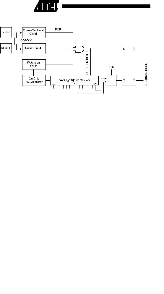
Figure 23. Reset Logic
Table 3. Reset Characteristics (VCC = 5.0V)
|
Symbol |
Parameter |
|
|
Min |
Typ |
Max |
Units |
||
|
(1) |
|
Power-on Reset Threshold Voltage (rising) |
1.0 |
1.4 |
1.8 |
V |
|||
|
|
|
|
|
|
|
|
|
|
|
|
VPOT |
|
Power-on Reset Threshold Voltage (falling) |
0.4 |
0.6 |
0.8 |
V |
|||
|
|
|
||||||||
|
|
|
|
|
|
|
|
|
|
|
|
VRST |
|
|
Pin Threshold Voltage |
|
– |
0.85 VCC |
V |
||
|
|
RESET |
|
|||||||
|
tTOUT |
|
Reset Delay Time-out Period |
11.0 |
16.0 |
21.0 |
ms |
|||
|
|
FSTRT Unprogrammed |
||||||||
|
tTOUT |
|
Reset Delay Time-out Period |
0.25 |
0.28 |
0.31 |
ms |
|||
|
|
FSTRT Programmed |
||||||||
|
Note: 1. |
The Power-on Reset will not work unless the supply voltage has been below VPOT |
||||||||
|
|
(falling). |
|
|
|
|
|
|
||
|
The user can select the start-up time according to typical oscillator start-up. The number |
|||||||||
|
of WDT oscillator cycles used for each time-out is shown in Table 4. The frequency of |
|||||||||
|
the Watchdog Oscillator is voltage-dependent, as shown in “Typical Characteristics” on |
|||||||||
|
page 75. |
|
|
|
|
|
|
|
|
|
|
Table 4. Number of Watchdog Oscillator Cycles |
|
|
|
|
|||||
|
FSTRT |
|
|
|
Time-out at VCC = 5V |
|
Number of WDT Cycles |
|
||
|
Programmed |
0.28 ms |
|
256 |
|
|
|
|||
|
|
|
|
|
|
|
|
|||
|
Unprogrammed |
16.0 ms |
|
16K |
|
|
|
|||
Power-on Reset |
|
|
|
|||||||
A Power-on Reset (POR) circuit ensures that the device is reset from power-on. As |
||||||||||
|
shown in Figure 23, an internal timer is clocked from the Watchdog Timer. This timer |
|||||||||
prevents the MCU from starting until after a certain period after VCC has reached the Power-on Threshold voltage (VPOT) (see Figure 24). The FSTRT Fuse bit in the Flash can be programmed to give a shorter start-up time if a ceramic resonator or any other fast-start oscillator is used to clock the MCU.
If the built-in start-up delay is sufficient, RESET can be connected to VCC directly or via an external pull-up resistor. By holding the RESET pin low for a period after VCC has been applied, the Power-on Reset period can be extended. Refer to Figure 25 for a timing example of this.
20 AT90S2313 
0839G–08/01
 AT90S2313
Figure 24. MCU Start-up, RESET Tied to VCC.
|
|
|
VCC |
|
|
VPOT |
|||||||||||||||||
|
|
|
|
|
|
|
|
|
|
|
|
|
|
|
|
|
|
|
|
||||
|
|
|
|
|
|
|
|
|
VRST |
||||||||||||||
|
|
RESET |
|
|
|||||||||||||||||||
|
|
|
|
|
|
|
|
|
|
|
|
|
|
|
|
|
|
|
|||||
|
TIME-OUT |
|
|
|
|
tTOUT |
|
|
|
|
|
|
|
|
|
||||||||
|
|
|
|
|
|
|
|
|
|
|
|
|
|
||||||||||
|
|
|
|
|
|
|
|
|
|
|
|
|
|
|
|||||||||
|
INTERNAL |
|
|
|
|
|
|
|
|
|
|
|
|
|
|
|
|
|
|||||
|
|
|
|
|
|
|
|
|
|
|
|
|
|
|
|
|
|
||||||
|
RESET |
|
|
|
|
|
|
|
|
|
|
|
|
|
|
|
|
|
|
||||
|
Figure 25. MCU Start-up, |
|
|
|
Controlled Externally |
||||||||||||||||||
|
RESET |
||||||||||||||||||||||
|
|
|
VCC |
|
|
VPOT |
|||||||||||||||||
|
|
|
|
|
|
|
|
|
|
|
|
|
|
|
|
|
|
|
|
||||
|
|
|
|
|
|
|
|
|
|
|
|
|
|
|
|
VRST |
|||||||
|
|
|
RESET |
|
|
|
|
|
|
|
|
||||||||||||
|
|
|
|
|
|
|
|
|
|
|
|
|
|
|
|
|
|
|
|
||||
|
TIME-OUT |
|
|
|
|
|
|
|
|
|
|
tTOUT |
|
|
|
|
|||||||
|
|
|
|
|
|
|
|
|
|
|
|
|
|
||||||||||
|
|
|
|
|
|
|
|
|
|
|
|
|
|
||||||||||
|
|
|
|
|
|
|
|
|
|
|
|
|
|
|
|
|
|
||||||
|
INTERNAL |
|
|
|
|
|
|
|
|
|
|
|
|
|
|
|
|
|
|||||
|
|
|
|
|
|
|
|
|
|
|
|
|
|
|
|
|
|
||||||
External Reset |
|
RESET |
|
|
|
|
|
|
|
|
|
|
|
|
|
|
|
|
|
||||
An external reset is generated by a low level on the |
|
|
|
pin. Reset pulses longer |
|||||||||||||||||||
RESET |
|||||||||||||||||||||||
|
than 50 ns will generate a reset, even if the clock is not running. Shorter pulses are not |
||||||||||||||||||||||
guaranteed to generate a reset. When the applied signal reaches the Reset Threshold Voltage (VRST) on its positive edge, the delay timer starts the MCU after the Time-out period tTOUT has expired.
Figure 26. External Reset during Operation
21
0839G–08/01
Watchdog Reset |
|
|
|
|
|
|
|
|
|
|
|
|
|
|
|
|
|
|
|
|
|
|
|
|
|
|
|
|
|
|
|
|
|
|
|
|
|
|
|
|
|
|
|
|
|
|
|
|
|
|
|
|
|
|
|
|
|
|
|
|
|
|
|
|
|
|
|
|
|
|
|
|
|
|
|
|
|
|
|
|
|
|
|
|
|
|
|
When the Watchdog times out, it will generate a short reset pulse of one XTAL cycle |
|||||||||||||||||||||
|
duration. On the falling edge of this pulse, the delay timer starts counting the Time-out |
||||||||||||||||||||
|
period tTOUT. Refer to page 38 for details on operation of the Watchdog. |
||||||||||||||||||||
|
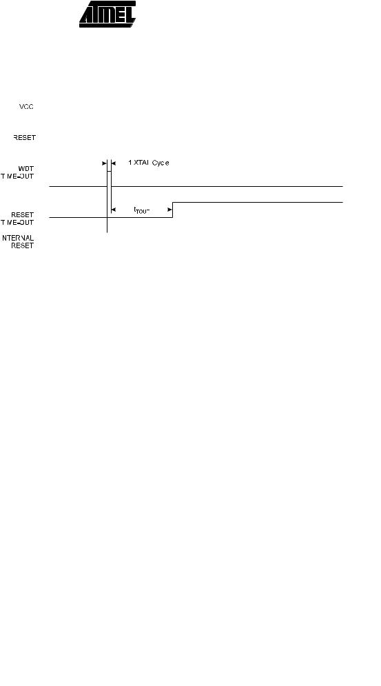
Figure 27. Watchdog Reset during Operation |
||||||||||||||||||||
|
|
|
|
|
|
|
|
|
|
|
|
|
|
|
|
|
|
|
|
|
|
|
|
|
|
|
|
|
|
|
|
|
|
|
|
|
|
|
|
|
|
|
|
|
|
|
|
|
|
|
|
|
|
|
|
|
|
|
|
|
|
|
|
|
|
|
|
|
|
|
|
|
|
|
|
|
|
|
|
|
|
|
|
|
|
|
|
|
|
|
|
|
|
|
|
|
|
|
|
|
|
|
|
|
|
|
|
|
|
|
|
|
|
|
|
|
|
|
|
|
|
|
|
|
|
|
|
|
|
|
|
|
|
|
|
|
|
|
|
|
|
|
|
|
|
|
|
|
|
|
|
|
|
|
|
|
|
|
|
|
|
|
|
|
|
|
|
|
|
|
|
|
|
|
|
|
|
|
|
|
|
|
|
|
|
|
|
|
|
|
|
|
|
|
|
|
|
|
|
|
|
|
|
|
|
|
|
|
|
|
|
|
|
|
|
|
|
|
|
|
|
|
|
|
|
|
|
|
|
|
|
|
|
|
|
|
|
|
|
|
|
|
|
|
|
|
|
|
|
|
|
|
|
|
|
|
|
|
|
|
|
|
|
Interrupt Handling |
The AT90S2313 has two 8-bit Interrupt Mask control registers: the GIMSK (General |
|
Interrupt Mask register) and the TIMSK (Timer/Counter Interrupt Mask register). |
|
When an interrupt occurs, the Global Interrupt Enable I-bit is cleared (zero) and all inter- |
|
rupts are disabled. The user software can set (one) the I-bit to enable interrupts. The I- |
|
bit is set (one) when a Return from Interrupt instruction (RETI) is executed. |
|
For interrupts triggered by events that can remain static (e.g., the Output Compare |
|
Register1 matching the value of Timer/Counter1), the interrupt flag is set when the event |
|
occurs. If the interrupt flag is cleared and the interrupt condition persists, the flag will not |
|
be set until the event occurs the next time. |
|
When the Program Counter is vectored to the actual interrupt vector in order to execute |
|
the interrupt handling routine, hardware clears the corresponding flag that generated the |
|
interrupt. Some of the interrupt flags can also be cleared by writing a logical “1” to the |
|
flag bit position(s) to be cleared. |
|
If an interrupt condition occurs when the corresponding interrupt enable bit is cleared |
|
(zero), the interrupt flag will be set and remembered until the interrupt is enabled, or the |
|
flag is cleared by software. |
|
If one or more interrupt conditions occur when the global interrupt enable bit is cleared |
|
(zero), the corresponding interrupt flag(s) will be set and remembered until the global |
|
interrupt enable bit is set (one), and will be executed by order of priority. |
|
Note that external level interrupt does not have a flag, and will only be remembered for |
|
as long as the interrupt condition is active. |
|
Note that the Status Register is not automatically stored when entering an interrupt rou- |
|
tine and restored when returning from an interrupt routine. This must be handled by |
|
software. |
22 AT90S2313 
0839G–08/01

General Interrupt Mask
Register – GIMSK
General Interrupt FLAG
Register – GIFR
AT90S2313
Bit |
7 |
6 |
5 |
4 |
3 |
2 |
1 |
0 |
|
$3B ($5B) |
INT1 |
INT0 |
– |
– |
– |
– |
– |
– |
GIMSK |
Read/Write |
R/W |
R/W |
R |
R |
R |
R |
R |
R |
|
Initial value |
0 |
0 |
0 |
0 |
0 |
0 |
0 |
0 |
|
• Bit 7 – INT1: External Interrupt Request 1 Enable
When the INT1 bit is set (one) and the I-bit in the Status Register (SREG) is set (one), the external pin interrupt is enabled. The Interrupt Sense Control1 bits 1/0 (ISC11 and ISC10) in the MCU general Control Register (MCUCR) defines whether the external interrupt is activated on rising or falling edge of the INT1 pin or level sensed. Activity on the pin will cause an interrupt request even if INT1 is configured as an output. The corresponding interrupt of External Interrupt Request 1 is executed from program memory address $002. See also “External Interrupts”.
• Bit 6 – INT0: External Interrupt Request 0 Enable
When the INT0 bit is set (one) and the I-bit in the Status Register (SREG) is set (one), the external pin interrupt is enabled. The Interrupt Sense Control0 bits 1/0 (ISC01 and ISC00) in the MCU general Control Register (MCUCR) defines whether the external interrupt is activated on rising or falling edge of the INT0 pin or level sensed. Activity on the pin will cause an interrupt request even if INT0 is configured as an output. The corresponding interrupt of External Interrupt Request 0 is executed from program memory address $001. See also “External Interrupts.”
• Bits 5..0 – Res: Reserved Bits
These bits are reserved bits in the AT90S2313 and always read as zero.
Bit |
7 |
6 |
5 |
4 |
3 |
2 |
1 |
0 |
|
$3A ($5A) |
INTF1 |
INTF0 |
– |
– |
– |
– |
– |
– |
GIFR |
Read/Write |
R/W |
R/W |
R |
R |
R |
R |
R |
R |
|
Initial value |
0 |
0 |
0 |
0 |
0 |
0 |
0 |
0 |
|
• Bit 7 – INTF1: External Interrupt Flag1
When an edge on the INT1 pin triggers an interrupt request, the corresponding interrupt flag, INTF1, becomes set (one). If the I-bit in SREG and the corresponding interrupt enable bit, INT1 bit in GIMSK, are set (one), the MCU will jump to the interrupt vector. The flag is cleared when the interrupt routine is executed. Alternatively, the flag can be cleared by writing a logical “1” to it. The flag is always cleared when INT1 is configured as level interrupt.
• Bit 6 – INTF0: External Interrupt Flag0
When an edge on the INT0 pin triggers an interrupt request, the corresponding interrupt flag, INTF0, becomes set (one). If the I-bit in SREG and the corresponding interrupt enable bit, INT0 bit in GIMSK, are set (one), the MCU will jump to the interrupt vector. The flag is cleared when the interrupt routine is executed. Alternatively, the flag can be cleared by writing a logical “1” to it. The flag is always cleared when INT0 is configured as level interrupt.
• Bits 5..0 – Res: Reserved Bits
These bits are reserved bits in the AT90S2313 and always read as zero.
Note that external level interrupt does not have a flag, and will only be remembered for as long as the interrupt condition is active.
23
0839G–08/01

Timer/Counter Interrupt Mask
Register – TIMSK
|
|
|
|
|
|
|
|
|
|
|
|
|
|
|
|
|
|
|
|
|
|
|
|
|
|
|
|
|
|
|
|
|
|
|
|
|
|
|
|
|
|
|
|
|
|
|
|
|
|
|
|
Bit |
7 |
6 |
|
5 |
4 |
3 |
2 |
1 |
0 |
|
||
$39 ($59) |
TOIE1 |
OCIE1A |
|
|
|
– |
– |
TICIE1 |
– |
TOIE0 |
– |
TIMSK |
Read/Write |
R/W |
R/W |
|
|
|
R |
R |
R/W |
R |
R/W |
R |
|
Initial value |
0 |
0 |
|
0 |
0 |
0 |
0 |
0 |
0 |
|
||
• Bit 7 – TOIE1: Timer/Counter1 Overflow Interrupt Enable
Timer/Counter Interrupt FLAG
Register – TIFR
When the TOIE1 bit is set (one) and the I-bit in the Status Register is set (one), the Timer/Counter1 Overflow Interrupt is enabled. The corresponding interrupt (at vector $005) is executed if an overflow in Timer/Counter1 occurs (i.e., when the TOV1 bit is set in the Timer/Counter Interrupt Flag Register [TIFR]).
• Bit 6 – OCIE1A: Timer/Counter1 Output Compare Match Interrupt Enable
When the OCIE1A bit is set (one) and the I-bit in the Status Register is set (one), the Timer/Counter1 Compare Match Interrupt is enabled. The corresponding interrupt (at vector $004) is executed if a compare match in Timer/Counter1 occurs (i.e., when the OCF1A bit is set in the Timer/Counter Interrupt Flag Register [TIFR]).
• Bit 5,4 – Res: Reserved Bits
These bits are reserved bits in the AT90S2313 and always read as zero.
• Bit 3 – TICIE1: Timer/Counter1 Input Capture Interrupt Enable
When the TICIE1 bit is set (one) and the I-bit in the Status Register is set (one), the Timer/Counter1 Input Capture Event Interrupt is enabled. The corresponding interrupt (at vector $003) is executed if a capture-triggering event occurs on PD6(ICP) (i.e., when the ICF1 bit is set in the Timer/Counter Interrupt Flag Register [TIFR]).
• Bit 2 – Res: Reserved Bit
This bit is a reserved bit in the AT90S2313 and always reads as zero.
• Bit 1 – TOIE0: Timer/Counter0 Overflow Interrupt Enable
When the TOIE0 bit is set (one) and the I-bit in the Status Register is set (one), the Timer/Counter0 Overflow Interrupt is enabled. The corresponding interrupt (at vector $006) is executed if an overflow in Timer/Counter0 occurs (i.e., when the TOV0 bit is set in the Timer/Counter Interrupt Flag Register [TIFR]).
• Bit 0 – Res: Reserved Bit
This bit is a reserved bit in the AT90S2313 and always read as zero.
Bit |
7 |
6 |
5 |
4 |
3 |
2 |
1 |
0 |
|
$38 ($58) |
TOV1 |
OCF1A |
– |
– |
ICF1 |
– |
TOV0 |
– |
TIFR |
Read/Write |
R/W |
R/W |
R |
R |
R/W |
R |
R/W |
R |
|
Initial value |
0 |
0 |
0 |
0 |
0 |
0 |
0 |
0 |
|
• Bit 7 – TOV1: Timer/Counter1 Overflow Flag
The TOV1 is set (one) when an overflow occurs in Timer/Counter1. TOV1 is cleared by hardware when executing the corresponding interrupt handling vector. Alternatively, TOV1 is cleared by writing a logical “1” to the flag. When the I-bit in SREG and TOIE1 (Timer/Counter1 Overflow Interrupt Enable) and TOV1 are set (one), the Timer/Counter1 Overflow Interrupt is executed. In PWM mode, this bit is set when Timer/Counter1 changes counting direction at $0000.
• Bit 6 – OCF1A: Output Compare Flag 1A
The OCF1A bit is set (one) when a compare match occurs between the Timer/Counter1 and the data in OCR1A (Output Compare Register1 A). OCF1A is cleared by hardware
24 AT90S2313 
0839G–08/01

 AT90S2313
when executing the corresponding interrupt handling vector. Alternatively, OCF1A is cleared by writing a logical “1” to the flag. When the I-bit in SREG and OCIE1A (Timer/Counter1 Compare Match Interrupt Enable) and the OCF1A are set (one), the
|
Timer/Counter1 Compare Match Interrupt is executed. |
|
• Bits 5, 4 – Res: Reserved Bits |
|
These bits are reserved bits in the AT90S2313 and always read as zero. |
|
• Bit 3 – ICF1: Input Capture Flag 1 |
|
The ICF1 bit is set (one) to flag an input capture event, indicating that the |
|
Timer/Counter1 value has been transferred to the Input Capture Register (ICR1). ICF1 |
|
is cleared by hardware when executing the corresponding interrupt handling vector. |
|
Alternatively, ICF1 is cleared by writing a logical “1” to the flag. When the SREG I-bit |
|
and TICIE1 (Timer/Counter1 Input Capture Interrupt Enable) and ICF1 are set (one), the |
|
Timer/Counter1 Capture Interrupt is executed. |
|
• Bit 2 – Res: Reserved Bit |
|
This bit is a reserved bit in the AT90S2313 and always reads as zero. |
|
• Bit 1 – TOV0: Timer/Counter0 Overflow Flag |
|
The bit TOV0 is set (one) when an overflow occurs in Timer/Counter0. TOV0 is cleared |
|
by hardware when executing the corresponding interrupt handling vector. Alternatively, |
|
TOV0 is cleared by writing a logical “1” to the flag. When the SREG I-bit and TOIE0 |
|
(Timer/Counter0 Overflow Interrupt Enable) and TOV0 are set (one), the |
|
Timer/Counter0 Overflow Interrupt is executed. |
|
• Bit 0 – Res: Reserved Bit |
|
This bit is a reserved bit in the AT90S2313 and always reads as zero. |
External Interrupts |
The External Interrupts are triggered by the INT1 and INT0 pins. Observe that, if |
|
enabled, the interrupts will trigger even if the INT0/INT1 pins are configured as outputs. |
|
This feature provides a way of generating a software interrupt. The External Interrupts |
|
can be triggered by a falling or rising edge or a low level. This is set up as indicated in |
|
the specification for the MCU Control Register (MCUCR). When the External Interrupt is |
|
enabled and is configured as level-triggered, the interrupt will trigger as long as the pin |
|
is held low. |
|
The External Interrupts are set up as described in the specification for the MCU Control |
|
Register (MCUCR). |
Interrupt Response Time |
The interrupt execution response for all the enabled AVR interrupts is four clock cycles, |
|
minimum. Four clock cycles after the interrupt flag has been set, the program vector |
|
address for the actual interrupt handling routine is executed. During this 4-clock-cycle |
|
period, the Program Counter (2 bytes) is pushed onto the stack, and the Stack Pointer is |
|
decremented by 2. The vector is normally a relative jump to the interrupt routine, and |
|
this jump takes two clock cycles. If an interrupt occurs during execution of a multi-cycle |
|
instruction, this instruction is completed before the interrupt is served. |
|
A return from an interrupt handling routine takes four clock cycles. During these four |
|
clock cycles, the Program Counter (2 bytes) is popped back from the stack, the Stack |
|
Pointer is incremented by 2, and the I-flag in SREG is set. When the AVR exits from an |
|
interrupt, it will always return to the main program and execute one more instruction |
|
before any pending interrupt is served. |
25
0839G–08/01

MCU Control Register –
MCUCR
The MCU Control Register contains control bits for general MCU functions.
Bit |
7 |
6 |
5 |
4 |
3 |
2 |
1 |
0 |
|
$35 ($55) |
– |
– |
SE |
SM |
ISC11 |
ISC10 |
ISC01 |
ISC00 |
MCUCR |
Read/Write |
R |
R |
R/W |
R/W |
R/W |
R/W |
R/W |
R/W |
|
Initial value |
0 |
0 |
0 |
0 |
0 |
0 |
0 |
0 |
|
• Bits 7, 6 – Res: Reserved Bits
These bits are reserved bits in the AT90S2313 and always read as zero.
• Bit 5 – SE: Sleep Enable
The SE bit must be set (one) to make the MCU enter the Sleep Mode when the SLEEP instruction is executed. To avoid the MCU entering the Sleep Mode unless it is the programmer’s purpose, it is recommended to set the Sleep Enable (SE) bit just before the execution of the SLEEP instruction.
• Bit 4 – SM: Sleep Mode
This bit selects between the two available sleep modes. When SM is cleared (zero), Idle Mode is selected as Sleep Mode. When SM is set (one), Power-down Mode is selected as Sleep Mode. For details, refer to the paragraph “Sleep Modes”.
• Bits 3, 2 – ISC11, ISC10: Interrupt Sense Control 1 Bit 1 and Bit 0
The External Interrupt 1 is activated by the external pin INT1 if the SREG I-flag and the corresponding interrupt mask in the GIMSK register is set. The level and edges on the external INT1 pin that activate the interrupt are defined in Table 5.
Table 5. Interrupt 1 Sense Control
ISC11 |
ISC10 |
Description |
|
|
|
0 |
0 |
The low level of INT1 generates an interrupt request. |
|
|
|
0 |
1 |
Reserved |
|
|
|
1 |
0 |
The falling edge of INT1 generates an interrupt request. |
|
|
|
1 |
1 |
The rising edge of INT1 generates an interrupt request. |
|
|
|
• Bits 1, 0 – ISC01, ISC00: Interrupt Sense Control 0 Bit 1 and Bit 0
The External Interrupt 0 is activated by the external pin INT0 if the SREG I-flag and the corresponding interrupt mask is set. The level and edges on the external INT0 pin that activate the interrupt are defined in Table 6.
Table 6. Interrupt 0 Sense Control
ISC01 |
ISC00 |
Description |
|
|
|
0 |
0 |
The low level of INT0 generates an interrupt request. |
|
|
|
0 |
1 |
Reserved |
|
|
|
1 |
0 |
The falling edge of INT0 generates an interrupt request. |
|
|
|
1 |
1 |
The rising edge of INT0 generates an interrupt request. |
|
|
|
The value on the INTn pin is sampled before detecting edges. If edge interrupt is selected, pulses with a duration longer than one CPU clock period will generate an interrupt. Shorter pulses are not guaranteed to generate an interrupt. If low-level interrupt is selected, the low level must be held until the completion of the currently executing instruction to generate an interrupt. If enabled, a level-triggered interrupt will generate an interrupt request as long as the pin is held low.
26 AT90S2313 
0839G–08/01

 AT90S2313
Sleep Modes
To enter the sleep modes, the SE bit in MCUCR must be set (one) and a SLEEP instruction must be executed. If an enabled interrupt occurs while the MCU is in a sleep mode, the MCU awakes, executes the interrupt routine, and resumes execution from the instruction following SLEEP. The contents of the register file, SRAM and I/O memory are unaltered. If a reset occurs during Sleep Mode, the MCU wakes up and executes from the Reset vector.
Idle Mode |
When the SM bit is cleared (zero), the SLEEP instruction forces the MCU into the Idle |
|
Mode, stopping the CPU but allowing Timer/Counters, Watchdog and the interrupt sys- |
|
tem to continue operating. This enables the MCU to wake up from external triggered |
|
interrupts as well as internal ones like Timer Overflow interrupt and Watchdog reset. If |
|
wake-up from the Analog Comparator Interrupt is not required, the Analog Comparator |
|
can be powered down by setting the ACD-bit in the Analog Comparator Control and Sta- |
|
tus Register (ACSR). This will reduce power consumption in Idle Mode. When the MCU |
|
wakes up from Idle Mode, the CPU starts program execution immediately. |
Power-down Mode |
When the SM bit is set (one), the SLEEP instruction forces the MCU into the Power- |
|
down Mode. In this mode, the external oscillator is stopped while the external interrupts |
|
and the Watchdog (if enabled) continue operating. Only an external reset, a Watchdog |
|
reset (if enabled), an external level interrupt on INT0 or INT1 can wake up the MCU. |
|
Note that when a level-triggered interrupt is used for wake-up from power-down, the low |
|
level must be held for a time longer than the reset delay Time-out period tTOUT. Other- |
|
wise, the device will not wake up. |
Timer/Counters |
The AT90S2313 provides two general-purpose Timer/Counters – one 8-bit T/C and one |
|
16-bit T/C. The Timer/Counters have individual prescaling selection from the same 10- |
|
bit prescaling timer. Both Timer/Counters can either be used as a timer with an internal |
|
clock time base or as a counter with an external pin connection that triggers the |
|
counting. |
27
0839G–08/01
Loading...