


ATMEL AT89C55-24JI, AT89C55-24JC, AT89C55-24AI, AT89C55-24AC, AT89C55-16QA Datasheet
...
Features
•Compatible with MCS-51™ Products
•20K Bytes of In-System Reprogrammable Flash Memory
–Endurance: 1,000 Write/Erase Cycles
•Fully Static Operation: 0 Hz to 33 MHz
•Three-Level Program Memory Lock
•256 x 8-bit Internal RAM
•32 Programmable I/O Lines
•Three 16-bit Timer/Counters
•Eight Interrupt Sources
•Low Power Idle and Power Down Modes
Description
The AT89C55 is a low-power, high-performance CMOS 8-bit microcomputer with 20K bytes of Flash programmable and erasable read only memory. The device is manufactured using Atmel’s high density nonvolatile memory technology and is compatible with the industry standard 80C51 instruction set and pinout. The on-chip Flash allows the program memory to be reprogrammed in-system or by a conventional nonvolatile memory programmer. By combining a versatile 8-bit CPU with Flash on a monolithic chip, the Atmel AT89C55 is a powerful microcomputer which provides a highly flexible and cost effective solution to many embedded control applications.
(continued)
Pin Configurations |
|
|
PDIP |
|||||
|
|
|
|
|
|
|
|
|
|
|
|
|
|
|
|
|
|
|
|
|
|
|
|
|
|
|
|
|
|
|
|
|
|
|
|
|
|
|
|
|
|
|
|
|
|
|
|
|
|
|
|
|
|
|
|
|
|
|
|
|
|
|
|
|
|
|
|
|
|
|
|
|
|
|
|
|
|
|
|
|
|
|
|
|
|
|
|
|
|
|
|
|
|
|
|
|
|
|
|
|
|
|
|
|
|
|
|
|
|
|
|
|
|
|
|
|
|
|
|
|
|
|
|
|
|
|
|
|
|
|
|
|
|
|
|
|
|
|
|
|
|
|
|
|
|
|
|
|
|
|
|
|
|
|
|
|
|
|
|
|
|
|
|
|
|
|
|
|
|
|
|
|
|
|
|
|
|
|
|
|
|
|
|
|
|
|
|
|
|
|
|
|
|
|
|
|
|
|
|
|
|
|
|
|
|
|
|
|
|
|
|
|
|
|
|
|
|
|
|
|
|
|
|
|
|
|
PQFP/TQFP |
|
|
|
|
|
|
|
|
|
PLCC |
||||||||||||||||||||||||||||||||||||||||||||||||||||||||||
|
|
|
|
|
|
|
|
|
|
|
|
|
|
|
|
|
|
|
|
|
|
|
|
|
|
|
|
|
|
|
|
|
|
|
|
|
|
|
|
|
|
|
|
|
|
|
|
|
|
|
|
|
|
|
|
|
|
|
|
|
|
|
|
|
|
|
|
|
|
|
|
|
|
|
|
|
|
|
|
|
|
|
|
|
|
|
|
|
|
|
|
|
|
|
|
|
|
|
|
|
|
|
|
|
|
|
|
|
|
|
|
|
|
|
|
|
|
|
|
|
|
|
|
|
|
|
|
|
|
|
|
|
|
|
|
|
|
|
|
|
|
|
|
|
|
|
|
|
|
|
|
|
|
|
|
|
|
|
|
|
|
|
|
|
|
|
|
|
|
|
|
|
|
|
|
|
|
|
|
|
|
|
|
|
|
|
|
|
|
|
|
|
|
|
|
|
|
|
|
|
|
|
|
|
|
|
|
|
|
|
|
|
|
|
|
|
|
|
|
|
|
|
|
|
|
|
|
|
|
|
|
|
|
|
|
|
|
|
|
|
|
|
|
|
|
|
|
|
|
|
|
|
|
|
|
|
|
|
|
|
|
|
|
|
|
|
|
|
|
|
|
|
|
|
|
|
|
|
|
|
|
|
|
|
|
|
|
|
|
|
|
|
|
|
|
|
|
|
|
|
|
|
|
|
|
|
|
|
|
|
|
|
|
|
|
|
|
|
|
|
|
|
|
|
|
|
|
|
|
|
|
|
|
|
|
|
|
|
|
|
|
|
|
|
|
|
|
|
|
|
|
|
|
|
|
|
|
|
|
|
|
|
|
|
|
|
|
|
|
|
|
|
|
|
|
|
|
|
|
|
|
|
|
|
|
|
|
|
|
|
|
|
|
|
|
|
|
|
|
|
|
|
|
|
|
|
|
|
|
|
|
|
|
|
|
|
|
|
|
|
|
|
|
|
|
|
|
|
|
|
|
|
|
|
|
|
|
|
|
|
|
|
|
|
|
|
|
|
|
|
|
|
|
|
|
|
|
|
|
|
|
|
|
|
|
|
|
|
|
|
|
|
|
|
|
|
|
|
|
|
|
|
|
|
|
|
|
|
|
|
|
|
|
|
|
|
|
|
|
|
|
|
|
|
|
|
|
|
|
|
|
|
|
|
|
|
|
|
|
|
|
|
|
|
|
|
|
|
|
|
|
|
|
|
|
|
|
|
|
|
|
|
|
|
|
|
|
|
|
|
|
|
|
|
|
|
|
|
|
|
|
|
|
|
|
|
|
|
|
|
|
|
|
|
|
|
|
|
|
|
|
|
|
|
|
|
|
|
|
|
|
|
|
|
|
|
|
|
|
|
|
|
|
|
|
|
|
|
|
|
|
|
|
|
|
|
|
|
|
|
|
|
|
|
|
|
|
|
|
|
|
|
|
|
|
|
|
|
|
|
|
|
|
|
|
|
|
|
|
|
|
|
|
|
|
|
|
|
|
|
|
|
|
|
|
|
|
|
|
|
|
|
|
|
|
|
|
|
|
|
|
|
|
|
|
|
|
|
|
|
|
|
|
|
|
|
|
|
|
|
|
|
|
|
|
|
|
|
|
|
|
|
|
|
|
|
|
|
|
|
|
|
|
|
|
|
|
|
|
|
|
|
|
|
|
|
|
|
|
|
|
|
|
|
|
|
|
|
|
|
|
|
|
|
|
|
|
|
|
|
|
|
|
|
|
|
|
|
|
|
|
|
|
|
|
|
|
|
|
|
|
|
|
|
|
|
|
|
|
|
|
|
|
|
|
|
|
|
|
|
|
|
|
|
|
|
|
|
|
|
|
|
|
|
|
|
|
|
|
|
|
|
|
|
|
|
|
|
|
|
|
|
|
|
|
|
|
|
|
|
|
|
|
|
|
|
|
|
|
|
|
|
|
|
|
|
|
|
|
|
|
|
|
|
|
|
|
|
|
|
|
|
|
|
|
|
|
|
|
|
|
|
|
|
|
|
|
|
|
|
|
|
|
|
|
|
|
|
|
|
|
|
|
|
|
|
|
|
|
|
|
|
|
|
|
|
|
|
|
|
|
|
|
|
|
|
|
|
|
|
|
|
|
|
|
|
|
|
|
|
|
|
|
|
|
|
|
|
|
|
|
|
|
|
|
|
|
|
|
|
|
|
|
|
|
|
|
|
|
|
|
|
|
|
|
|
|
|
|
|
|
|
|
|
|
|
|
|
|
|
|
|
|
|
|
|
|
|
|
|
|
|
|
|
|
|
|
|
|
|
|
|
|
|
|
|
|
|
|
|
|
|
|
|
|
|
|
|
|
|
|
|
|
|
|
|
|
|
|
|
|
|
|
|
|
|
|
|
|
|
|
|
|
|
|
|
|
|
|
|
|
|
|
|
|
|
|
|
|
|
|
|
|
|
|
|
|
|
|
|
|
|
|
|
|
|
|
|
|
|
|
|
|
|
|
|
|
|
|
|
|
|
|
|
|
|
|
|
|
|
|
|
|
|
|
|
|
|
|
|
|
|
|
|
|
|
|
|
|
|
|
|
|
|
|
|
|
|
|
|
|
|
|
|
|
|
|
|
|
|
|
|
|
|
|
|
|
|
|
|
|
|
|
|
|
|
|
|
|
|
|
|
|
|
|
|
|
|
|
|
|
|
|
|
|
|
|
|
|
|
|
|
|
|
|
|
|
|
|
|
|
|
|
|
|
|
|
|
|
|
|
|
|
|
|
|
|
|
|
|
|
|
|
|
|
|
|
|
|
|
|
|
|
|
|
|
|
|
|
|
|
|
|
|
|
|
|
|
|
|
|
|
|
|
|
|
|
|
|
|
|
|
|
|
|
|
|
|
|
|
|
|
|
|
|
|
|
|
|
|
|
|
|
|
|
|
|
|
|
|
|
|
|
|
|
|
|
|
|
|
|
|
|
|
|
|
|
|
|
|
|
|
|
|
|
|
|
|
|
|
|
|
|
|
|
|
|
|
|
|
|
|
|
|
|
|
|
|
|
|
|
|
|
|
|
|
|
|
|
|
|
|
|
|
|
|
|
|
|
|
|
|
|
|
|
|
|
|
|
|
|
|
|
|
|
|
|
|
|
|
|
|
|
|
|
|
|
|
|
|
|
|
|
|
|
|
|
|
|
|
|
|
|
|
|
|
|
|
|
|
|
|
|
|
|
|
|
|
|
|
|
|
|
|
|
|
|
|
|
|
|
|
|
|
|
|
|
|
|
|
|
|
|
|
|
|
|
|
|
|
|
|
|
|
|
|
|
|
|
|
|
|
|
|
|
|
|
|
|
|
|
|
|
|
|
|
|
|
|
|
|
|
|
|
|
|
|
|
|
|
|
|
|
|
|
|
|
|
|
|
|
|
|
|
|
|
|
|
|
|
|
|
|
|
|
|
|
|
|
|
|
|
|
|
|
|
|
|
|
|
|
|
|
|
|
|
|
|
|
|
|
|
|
|
|
|
|
|
|
|
|
|
|
|
|
|
|
|
|
|
|
|
|
|
|
|
|
|
|
|
|
|
|
|
|
|
|
|
|
|
|
|
|
|
|
|
|
|
|
|
|
|
|
|
|
|
|
|
|
|
|
|
|
|
|
|
|
|
|
|
|
|
|
|
|
|
|
|
|
|
|
|
|
|
|
|
|
|
|
|
|
|
|
|
|
|
|
|
|
|
|
|
|
|
|
|
|
|
|
|
|
|
|
|
|
|
|
|
|
|
|
|
|
|
|
|
|
|
|
|
|
|
|
|
|
|
|
|
|
|
|
|
|
|
|
|
|
|
|
|
|
|
|
|
|
|
|
|
|
|
|
|
|
|
|
|
|
|
|
|
|
|
|
|
|
|
|
|
|
|
|
|
|
|
|
|
|
|
|
|
|
|
|
|
|
|
|
|
|
|
|
|
|
|
|
|
|
|
|
|
|
|
|
|
|
|
|
|
|
AT89C55 |
8-Bit |
Microcontroller |
with 20K Bytes |
Flash |
AT89C55 |
0580D-A–12/97 |
4-169 |
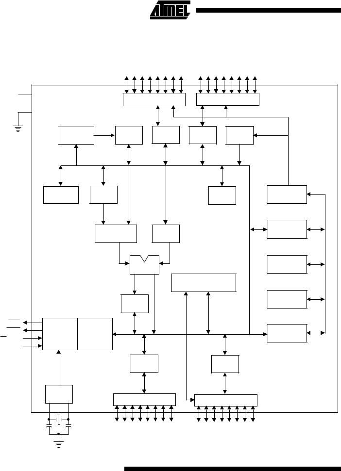
Block Diagram |
|
|
|
|
|
|
|
|
|
|
P0.0 |
- P0.7 |
P2.0 - |
P2.7 |
|
VCC |
|
|
|
|
|
|
|
|
|
|
PORT 0 DRIVERS |
PORT 2 DRIVERS |
|
||
GND |
|
|
|
|
|
|
|
|
RAM ADDR. |
RAM |
PORT 0 |
PORT 2 |
FLASH |
|
|
|
REGISTER |
|
LATCH |
LATCH |
|
||
|
|
|
|
||||
|
B |
|
|
|
STACK |
|
PROGRAM |
|
|
ACC |
|
|
ADDRESS |
||
|
REGISTER |
|
POINTER |
||||
|
|
|
|
|
|
|
REGISTER |
|
|
|
|
|
|
|
BUFFER |
|
|
|
TMP2 |
TMP1 |
|
|
|
|
|
|
|
|
|
|
PC |
|
|
|
ALU |
|
|
|
INCREMENTER |
|
|
|
|
INTERRUPT, SERIAL PORT, |
|
||
|
|
|
|
|
AND TIMER BLOCKS |
|
|
|
|
|
|
|
|
|
PROGRAM |
|
|
|
PSW |
|
|
|
COUNTER |
PSEN |
|
|
|
|
|
|
|
ALE/PROG |
TIMING |
INSTRUCTION |
|
|
|
DPTR |
|
AND |
|
|
|
||||
EA / VPP |
REGISTER |
|
|
|
|||
CONTROL |
|
|
|
|
|||
|
|
|
|
|
|
||
RST |
|
|
|
|
|
|
|
|
|
|
PORT 1 |
PORT 3 |
|
||
|
|
|
LATCH |
|
LATCH |
|
|
|
OSC |
|
|
|
|
|
|
|
|
|
PORT 1 DRIVERS |
PORT 3 DRIVERS |
|
||
|
|
|
P1.0 - P1.7 |
P3.0 - |
P3.7 |
|
|
|
|
|
|
|
|
||
4-170 |
|
AT89C55 |
|
|
|
|
|

The AT89C55 provides the following standard features: 20K bytes of Flash, 256-bytes of RAM, 32 I/O lines, three 16-bit timer/counters, a six-vector two-level interrupt architecture, a full duplex serial port, on-chip oscillator, and clock circuitry. In addition, the AT89C55 is designed with static logic for operation down to zero frequency and supports two software selectable power saving modes. The Idle Mode stops the CPU while allowing the RAM, timer/counters, serial port, and interrupt system to continue functioning. The Power Down Mode saves the RAM contents but freezes the oscillator, disabling all other chip functions until the next hardware reset. The low-voltage option saves power and operates with a 2.7-volt power supply.
Pin Description
VCC
Supply voltage.
GND
Ground.
Port 0
Port 0 is an 8-bit open drain bidirectional I/O port. As an output port, each pin can sink eight TTL inputs. When 1s are written to port 0 pins, the pins can be used as highimpedance inputs.
Port 0 can also be configured to be the multiplexed loworder address/data bus during accesses to external program and data memory. In this mode, P0 has internal pullups.
Port 0 also receives the code bytes during Flash programming and outputs the code bytes during program verification. External pullups are required during program verification.
Port 1
Port 1 is an 8-bit bidirectional I/O port with internal pullups. The Port 1 output buffers can sink/source four TTL inputs. When 1s are written to Port 1 pins, they are pulled high by the internal pullups and can be used as inputs. As inputs, Port 1 pins that are externally being pulled low will source current (IIL) because of the internal pullups.
In addition, P1.0 and P1.1 can be configured to be the timer/counter 2 external count input (P1.0/T2) and the timer/counter 2 trigger input (P1.1/T2EX), respectively, as shown in the following table.
Port Pin Alternate Functions
P1.0
T2 (external count input to Timer/Counter 2), clock-out
P1.1
T2EX (Timer/Counter 2 capture/reload trigger and direction control)
AT89C55
Port 2
Port 2 is an 8-bit bidirectional I/O port with internal pullups. The Port 2 output buffers can sink/source four TTL inputs. When 1s are written to Port 2 pins, they are pulled high by the internal pullups and can be used as inputs. As inputs, Port 2 pins that are externally being pulled low will source current (IIL) because of the internal pullups.
Port 2 emits the high-order address byte during fetches from external program memory and during accesses to external data memory that use 16-bit addresses (MOVX @ DPTR). In this application, Port 2 uses strong internal pullups when emitting 1s. During accesses to external data memory that use 8-bit addresses (MOVX @ RI), Port 2 emits the contents of the P2 Special Function Register.
Port 2 also receives the high-order address bits and some control signals during Flash programming and verification.
Port 3
Port 3 is an 8-bit bidirectional I/O port with internal pullups. The Port 3 output buffers can sink/source four TTL inputs. When 1s are written to Port 3 pins, they are pulled high by the internal pullups and can be used as inputs. As inputs, Port 3 pins that are externally being pulled low will source current (IIL) because of the pullups.
Port 3 also serves the functions of various special features of the AT89C55, as shown in the following table.
Port Pin |
|
Alternate Functions |
|||
|
|
|
|||
P3.0 |
|
RXD (serial input port) |
|||
|
|
|
|||
P3.1 |
|
TXD (serial output port) |
|||
|
|
|
|
|
|
P3.2 |
|
|
|
|
(external interrupt 0) |
|
INT0 |
||||
|
|
|
|
|
|
P3.3 |
|
|
|
|
(external interrupt 1) |
|
INT1 |
||||
|
|
|
|||
P3.4 |
|
T0 (timer 0 external input) |
|||
|
|
|
|||
P3.5 |
|
T1 (timer 1 external input) |
|||
|
|
|
|
|
|
P3.6 |
|
|
|
(external data memory write strobe) |
|
WR |
|||||
|
|
|
|
||
P3.7 |
|
|
(external data memory read strobe) |
||
|
RD |
||||
|
|
|
|
|
|
Port 3 also receives the highest-order address bit and some control signals for Flash programming and verification.
RST
Reset input. A high on this pin for two machine cycles while the oscillator is running resets the device.
Port 1 also receives the low-order address bytes during
Flash programming and verification.
4-171

ALE/PROG
Address Latch Enable is an output pulse for latching the low byte of the address during accesses to external memory. This pin is also the program pulse input (PROG) during Flash programming.
In normal operation, ALE is emitted at a constant rate of 1/6 the oscillator frequency and may be used for external timing or clocking purposes. Note, however, that one ALE pulse is skipped during each access to external data memory.
If desired, ALE operation can be disabled by setting bit 0 of SFR location 8EH. With the bit set, ALE is active only during a MOVX or MOVC instruction. Otherwise, the pin is weakly pulled high. Setting the ALE-disable bit has no effect if the microcontroller is in external execution mode.
PSEN
Program Store Enable is the read strobe to external program memory.
When the AT89C55 is executing code from external program memory, PSEN is activated twice each machine cycle, except that two PSEN activations are skipped during each access to external data memory.
EA/VPP
External Access Enable. EA must be strapped to GND in order to enable the device to fetch code from external program memory locations starting at 0000H up to FFFFH. Note, however, that if lock bit 1 is programmed, EA will be internally latched on reset.
EA should be strapped to VCC for internal program executions.
This pin also receives the 12-volt programming enable voltage (VPP) during 12-volt Flash programming.
XTAL1
Input to the inverting oscillator amplifier and input to the internal clock operating circuit.
XTAL2
Output from the inverting oscillator amplifier.
Special Function Registers
A map of the on-chip memory area called the Special Function Register (SFR) space is shown in Table 1.
Note that not all of the addresses are occupied, and unoccupied addresses may not be implemented on the chip. Read accesses to these addresses will in general return random data, and write accesses will have an indeterminate effect.
User software should not write 1s to these unlisted locations, since they may be used in future products to invoke new features. In that case, the reset or inactive values of the new bits will always be 0.
Timer 2 Registers Control and status bits are contained in registers T2CON (shown in Table 2) and T2MOD (shown in Table 4) for Timer 2. The register pair (RCAP2H, RCAP2L) are the Capture/Reload registers for Timer 2 in 16 bit capture mode or 16-bit auto-reload mode.
Interrupt Registers The individual interrupt enable bits are in the IE register. Two priorities can be set for each of the six interrupt sources in the IP register.
Data Memory
The AT89C55 implements 256-bytes of on-chip RAM. The upper 128-bytes occupy a parallel address space to the Special Function Registers. That means the upper 128bytes have the same addresses as the SFR space but are physically separate from SFR space.
When an instruction accesses an internal location above address 7FH, the address mode used in the instruction specifies whether the CPU accesses the upper 128-bytes of RAM or the SFR space. Instructions that use direct addressing access SFR space.
For example, the following direct addressing instruction accesses the SFR at location 0A0H (which is P2).
MOV 0A0H, #data
Instructions that use indirect addressing access the upper 128-bytes of RAM. For example, the following indirect addressing instruction, where R0 contains 0A0H, accesses the data byte at address 0A0H, rather than P2 (whose address is 0A0H).
MOV @R0, #data
Note that stack operations are examples of indirect addressing, so the upper 128-bytes of data RAM are available as stack space.
4-172 |
AT89C55 |
|
|
||
|

|
|
|
|
|
|
|
|
|
AT89C55 |
|
|
|
|
|
|
|
|
|
|
|
|
||
Table 1. AT89C55 SFR Map and Reset Values |
|
|
|
|
|
||||||
|
|
|
|
|
|
|
|||||
|
0F8H |
|
|
|
|
|
|
|
|
|
0FFH |
|
|
|
|
|
|
|
|
|
|
||
|
|
|
|
|
|
|
|
|
|
|
|
|
0F0H |
B |
|
|
|
|
|
|
|
|
0F7H |
|
00000000 |
|
|
|
|
|
|
|
|
||
|
|
|
|
|
|
|
|
|
|
|
|
|
0E8H |
|
|
|
|
|
|
|
|
|
0EFH |
|
|
|
|
|
|
|
|
|
|
||
|
|
|
|
|
|
|
|
|
|
|
|
|
0E0H |
ACC |
|
|
|
|
|
|
|
|
0E7H |
|
00000000 |
|
|
|
|
|
|
|
|
||
|
|
|
|
|
|
|
|
|
|
|
|
|
0D8H |
|
|
|
|
|
|
|
|
|
0DFH |
|
|
|
|
|
|
|
|
|
|
||
|
|
|
|
|
|
|
|
|
|
|
|
|
0D0H |
PSW |
|
|
|
|
|
|
|
|
0D7H |
|
00000000 |
|
|
|
|
|
|
|
|
||
|
|
|
|
|
|
|
|
|
|
|
|
|
|
|
|
|
|
|
|
|
|
|
|
|
0C8H |
T2CON |
T2MOD |
RCAP2L |
RCAP2H |
TL2 |
TH2 |
|
|
|
0CFH |
|
00000000 |
XXXXXX00 |
00000000 |
00000000 |
00000000 |
00000000 |
|
|
|
||
|
|
|
|
|
|
||||||
|
0C0H |
|
|
|
|
|
|
|
|
|
0C7H |
|
|
|
|
|
|
|
|
|
|
||
|
|
|
|
|
|
|
|
|
|
|
|
|
0B8H |
IP |
|
|
|
|
|
|
|
|
0BFH |
|
XX000000 |
|
|
|
|
|
|
|
|
||
|
|
|
|
|
|
|
|
|
|
|
|
|
|
|
|
|
|
|
|
|
|
|
|
|
0B0H |
P3 |
|
|
|
|
|
|
|
|
0B7H |
|
11111111 |
|
|
|
|
|
|
|
|
||
|
|
|
|
|
|
|
|
|
|
|
|
|
|
|
|
|
|
|
|
|
|
|
|
|
0A8H |
IE |
|
|
|
|
|
|
|
|
0AFH |
|
0X000000 |
|
|
|
|
|
|
|
|
||
|
|
|
|
|
|
|
|
|
|
|
|
|
|
|
|
|
|
|
|
|
|
|
|
|
0A0H |
P2 |
|
|
|
|
|
|
|
|
0A7H |
|
11111111 |
|
|
|
|
|
|
|
|
||
|
|
|
|
|
|
|
|
|
|
|
|
|
|
|
|
|
|
|
|
|
|
|
|
|
98H |
SCON |
SBUF |
|
|
|
|
|
|
|
9FH |
|
00000000 |
XXXXXXXX |
|
|
|
|
|
|
|
||
|
|
|
|
|
|
|
|
|
|
||
|
|
|
|
|
|
|
|
|
|
|
|
|
90H |
P1 |
|
|
|
|
|
|
|
|
97H |
|
11111111 |
|
|
|
|
|
|
|
|
||
|
|
|
|
|
|
|
|
|
|
|
|
|
|
|
|
|
|
|
|
|
|
|
|
|
88H |
TCON |
TMOD |
TL0 |
TL1 |
TH0 |
TH1 |
|
|
|
8FH |
|
00000000 |
00000000 |
00000000 |
00000000 |
00000000 |
00000000 |
|
|
|
||
|
|
|
|
|
|
||||||
|
|
|
|
|
|
|
|
|
|
|
|
|
80H |
P0 |
SP |
DPL |
DPH |
|
|
|
|
PCON |
87H |
|
11111111 |
00000111 |
00000000 |
00000000 |
|
|
|
|
0XXX0000 |
||
|
|
|
|
|
|
|
|||||
|
|
|
|
|
|
|
|
|
|
|
|
4-173

Table 2. T2CON—Timer/Counter 2 Control Register
|
|
T2CON Address = 0C8H |
|
|
|
|
|
|
|
|
|
|
|
Reset Value = 0000 0000B |
||||||||||||||
|
|
Bit Addressable |
|
|
|
|
|
|
|
|
|
|
|
|
|
|
|
|
|
|
|
|
|
|
||||
|
|
|
|
|
|
|
|
|
|
|
|
|
|
|
|
|
|
|
|
|
|
|
||||||
|
|
|
|
|
|
TF2 |
EXF2 |
|
RCLK |
TCLK |
EXEN2 |
TR2 |
|
|
|
|
|
|
|
|
|
|
|
|||||
|
|
|
|
|
|
C/T2 |
|
|
CP/RL2 |
|
||||||||||||||||||
|
|
|
|
|
|
|
|
|
|
|
|
|
|
|
|
|
|
|
|
|
|
|||||||
|
|
Bit |
|
7 |
6 |
|
5 |
4 |
3 |
|
|
2 |
|
1 |
|
|
0 |
|
|
|
|
|||||||
|
|
|
|
|
|
|
|
|
|
|
|
|
|
|
|
|
|
|
|
|
|
|
|
|
||||
|
|
|
|
|
|
|
|
|
|
|
|
|
|
|
|
|
|
|
|
|
|
|
|
|||||
Symbol |
Function |
|
|
|
|
|
|
|
|
|
|
|
|
|
|
|
|
|
|
|
|
|
|
|||||
|
|
|||||||||||||||||||||||||||
TF2 |
Timer 2 overflow flag set by a Timer 2 overflow and must be cleared by software. TF2 will not be set when either RCLK |
|||||||||||||||||||||||||||
|
|
|
|
|
= 1 or TCLK = 1. |
|
|
|
|
|
|
|
|
|
|
|
|
|
|
|
|
|
|
|
|
|
|
|
|
|
|||||||||||||||||||||||||||
EXF2 |
Timer 2 external flag set when either a capture or reload is caused by a negative transition on T2EX and EXEN2 = 1. |
|||||||||||||||||||||||||||
|
|
|
|
|
When Timer 2 interrupt is enabled, EXF2 = 1 will cause the CPU to vector to the Timer 2 interrupt routine. EXF2 must |
|||||||||||||||||||||||
|
|
|
|
|
be cleared by software. EXF2 does not cause an interrupt in up/down counter mode (DCEN = 1). |
|
|
|
|
|
|
|||||||||||||||||
|
|
|||||||||||||||||||||||||||
RCLK |
Receive clock enable. When set, causes the serial port to use Timer 2 overflow pulses for its receive clock in serial port |
|||||||||||||||||||||||||||
|
|
|
|
|
Modes 1 and 3. RCLK = 0 causes Timer 1 overflow to be used for the receive clock. |
|
|
|
|
|
|
|||||||||||||||||
|
|
|||||||||||||||||||||||||||
TCLK |
Transmit clock enable. When set, causes the serial port to use Timer 2 overflow pulses for its transmit clock in serial |
|||||||||||||||||||||||||||
|
|
|
|
|
port Modes 1 and 3. TCLK = 0 causes Timer 1 overflows to be used for the transmit clock. |
|
|
|
|
|
|
|||||||||||||||||
|
|
|||||||||||||||||||||||||||
EXEN2 |
Timer 2 external enable. When set, allows a capture or reload to occur as a result of a negative transition on T2EX if |
|||||||||||||||||||||||||||
|
|
|
|
|
Timer 2 is not being used to clock the serial port. EXEN2 = 0 causes Timer 2 to ignore events at T2EX. |
|||||||||||||||||||||||
|
|
|
|
|
|
|
|
|
|
|
|
|
|
|
|
|
||||||||||||
TR2 |
Start/Stop control for Timer 2. TR2 = 1 starts the timer. |
|
|
|
|
|
|
|
|
|
|
|
|
|
|
|
||||||||||||
|
|
|
|
|
|
|
|
|
|
|
|
|
|
|
|
|
|
|
|
|
||||||||
|
|
|
|
|
|
|
|
|
|
|
|
|
|
|
|
|
|
|
|
|
|
|
|
|
|
|
|
|
C/T2 |
|
|
Timer or counter select for Timer 2. C/T2 = 0 for timer function. C/T2 = 1 for external event counter (falling edge |
|||||||||||||||||||||||||
|
|
|
|
|
triggered). |
|
|
|
|
|
|
|
|
|
|
|
|
|
|
|
|
|
|
|
|
|
|
|
|
|
|
|
|
|
|
|
|
|
|
|
|
|
|
||||||||||||||
|
|
|
|
|
|
|
|
|
|
|
|
|
|
|
|
|
|
|
|
|
|
|
|
|
|
|
|
|
CP/RL2 |
Capture/Reload select. CP/RL2 |
= 1 causes captures to occur on negative transitions at T2EX if EXEN2 = 1. CP/RL2 = |
||||||||||||||||||||||||||
|
|
|
|
|
0 causes automatic reloads to occur when Timer 2 overflows or negative transitions occur at T2EX when EXEN2 = 1. |
|||||||||||||||||||||||
|
|
|
|
|
When either RCLK or TCLK = 1, this bit is ignored and the timer is forced to auto-reload on Timer 2 overflow. |
|||||||||||||||||||||||
|
|
|
|
|
|
|
|
|
|
|
|
|
|
|
|
|
|
|
|
|
|
|
|
|
|
|
|
|
4-174 |
AT89C55 |
|
|
||
|
Timer 0 and 1
Timer 0 and Timer 1 in the AT89C55 operate the same way as Timer) and Timer 1 in the AT89C51 and AT89C52. For further information, see the Microcontroller Data Book, section titled, “Timer/Counters.”
Timer 2
Timer 2 is a 16 bit Timer/Counter that can operate as either a timer or an event counter. The type of operation is selected by bit C/T2 in the SFR T2CON (shown in Table 2). Timer 2 has three operating modes: capture, auto-reload (up or down counting), and baud rate generator. The modes are selected by bits in T2CON, as shown in Table 3.
Timer 2 consists of two 8-bit registers, TH2 and TL2. In the Timer function, the TL2 register is incremented every machine cycle. Since a machine cycle consists of 12 oscillator periods, the count rate is 1/12 of the oscillator frequency.
In the Counter function, the register is incremented in response to a 1-to-0 transition at its corresponding external input pin, T2. In this function, the external input is sampled during S5P2 of every machine cycle. When the samples
Table 3. Timer 2 Operating Modes
|
|
|
|
|
|
RCLK + TCLK |
CP/RL2 |
TR2 |
MODE |
||
|
|
|
|
|
|
0 |
0 |
|
1 |
16 bit Auto-Reload |
|
|
|
|
|
|
|
0 |
1 |
|
1 |
16 bit Capture |
|
|
|
|
|
|
|
1 |
X |
1 |
Baud Rate Generator |
||
|
|
|
|
|
|
X |
X |
0 |
(Off) |
||
|
|
|
|
|
|
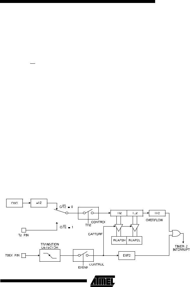
Figure 1. Timer 2 in Capture Mode
AT89C55
show a high in one cycle and a low in the next cycle, the count is incremented. The new count value appears in the register during S3P1 of the cycle following the one in which the transition was detected. Since two machine cycles (24 oscillator periods) are required to recognize a 1-to-0 transition, the maximum count rate is 1/24 of the oscillator frequency. To ensure that a given level is sampled at least once before it changes, the level should be held for at least one full machine cycle.
Capture Mode
In the capture mode, two options are selected by bit EXEN2 in T2CON. If EXEN2 = 0, Timer 2 is a 16 bit timer or counter which upon overflow sets bit TF2 in T2CON. This bit can then be used to generate an interrupt. If EXEN2 = 1, Timer 2 performs the same operation, but a 1- to-0 transition at external input T2EX also causes the current value in TH2 and TL2 to be captured into RCAP2H and RCAP2L, respectively. In addition, the transition at T2EX causes bit EXF2 in T2CON to be set. The EXF2 bit, like TF2, can generate an interrupt. The capture mode is illustrated in Figure 1.
Auto-Reload (Up or Down Counter)
Timer 2 can be programmed to count up or down when configured in its 16-bit auto-reload mode. This feature is invoked by the DCEN (Down Counter Enable) bit located in the SFR T2MOD (see Table 4). Upon reset, the DCEN bit is set to 0 so that timer 2 will default to count up. When DCEN is set, Timer 2 can count up or down, depending on the value of the T2EX pin.
Figure 2 shows Timer 2 automatically counting up when DCEN = 0. In this mode, two options are selected by bit EXEN2 in T2CON. If EXEN2 = 0, Timer 2 counts up to 0FFFFH and then sets the TF2 bit upon overflow. The overflow also causes the timer registers to be reloaded with the 16 bit value in RCAP2H and RCAP2L. The values in RCAP2H and RCAP2L are preset by software. If EXEN2 =
4-175
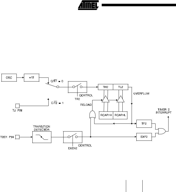
1, a 16 bit reload can be triggered either by an overflow or by a 1-to-0 transition at external input T2EX. This transition also sets the EXF2 bit. Both the TF2 and EXF2 bits can generate an interrupt if enabled.
Setting the DCEN bit enables Timer 2 to count up or down, as shown in Figure 3. In this mode, the T2EX pin controls the direction of the count. A logic 1 at T2EX makes Timer 2 count up. The timer will overflow at 0FFFFH and set the TF2 bit. This overflow also causes the 16 bit value in
Figure 2. Timer 2 Auto Reload Mode (DCEN = 0)
RCAP2H and RCAP2L to be reloaded into the timer registers, TH2 and TL2, respectively.
A logic 0 at T2EX makes Timer 2 count down. The timer underflows when TH2 and TL2 equal the values stored in RCAP2H and RCAP2L. The underflow sets the TF2 bit and causes 0FFFFH to be reloaded into the timer registers.
The EXF2 bit toggles whenever Timer 2 overflows or underflows and can be used as a 17th bit of resolution. In this operating mode, EXF2 does not flag an interrupt.
Table 4. T2MOD—Timer 2 Mode Control Register
T2MOD Address = 0C9H |
|
|
|
|
|
Reset Value = XXXX XX00B |
|
|||
Not Bit Addressable |
|
|
|
|
|
|
|
|
||
|
|
|
|
|
|
|
|
|
|
|
|
|
— |
— |
— |
— |
— |
— |
T20E |
DCEN |
|
|
|
|
|
|
|
|
|
|
|
|
Bit |
|
7 |
6 |
5 |
4 |
3 |
2 |
1 |
0 |
|
|
|
|
|
|
|
|
|
|
|
|
|
|
|
|
|
|
|
|
|
|
|
Symbol |
Function |
|
|
|
|
|
|
|
|
|
|
|
|
|
|
|
|
|
|||
— |
Not implemented, reserved for future use. |
|
|
|
|
|
|
|||
|
|
|
|
|
|
|
|
|
||
T20E |
Timer 2 Output Enable bit. |
|
|
|
|
|
|
|
||
|
|
|
|
|
||||||
DCEN |
When set, this bit allows Timer 2 to be configured as an up/down counter. |
|
|
|
||||||
|
|
|
|
|
|
|
|
|
|
|
4-176 |
AT89C55 |
|
|
||
|
 Loading...