


ATMEL AT49LV001N-70JI, AT49LV001N-12VI, AT49LV001N-12VC, AT49LV001N-12TI, AT49LV001N-12TC Datasheet
...
Features
•Single Supply for Read and Write: 2.7V to 3.6 (BV), 3.0 to 3.6V (LV)
•Fast Read Access Time - 70 ns
•Internal Program Control and Timer
•Sector Architecture
–One 16K Byte Boot Block with Programming Lockout
–Two 8K Byte Parameter Blocks
–Two Main Memory Blocks (32K, 64K) Bytes
•Fast Erase Cycle Time - 10 seconds
•Byte By Byte Programming - 30 μs/Byte Typical
•Hardware Data Protection
•DATA Polling For End Of Program Detection
•Low Power Dissipation
–25 mA Active Current
–50 μA CMOS Standby Current
•Typical 10,000 Write Cycles
Description
The AT49BV/LV001(N)(T) is a 3-volt-only in-system reprogrammable Flash Memory. Its 1 megabit of memory is organized as 131,072 words by 8 bits. Manufactured with Atmel’s advanced nonvolatile CMOS technology, the device offers access times to 70 ns with power dissipation of just 90 mW over the commercial temperature range. When the device is deselected, the CMOS standby current is less than 50 μA. For the
Pin Configurations
|
Pin Name |
|
|
Function |
|
|
|
||||||||||
|
|
|
|
|
|
|
|
|
|
||||||||
|
A0 - A16 |
|
|
Addresses |
|
|
|
||||||||||
|
|
|
|
|
|
|
|
|
|
|
|
|
|
|
|||
|
|
|
|
|
|
|
|
|
Chip Enable |
|
|
|
|||||
|
CE |
|
|
|
|
|
|
|
|||||||||
|
|
|
|
|
|
|
|
|
|
|
|
|
|||||
|
|
|
|
|
|
|
|
|
Output Enable |
||||||||
|
OE |
|
|
|
|
||||||||||||
|
|
|
|
|
|
|
|
|
|
|
|
|
|||||
|
|
|
|
|
|
|
|
|
Write Enable |
|
|
|
|||||
|
WE |
|
|
|
|
|
|
|
|||||||||
|
|
|
|
|
|
|
|
|
|
|
|
||||||
|
|
|
|
|
|
|
|
|
RESET |
|
|
|
|
||||
|
RESET |
|
|
|
|
|
|
||||||||||
|
|
|
|
|
|
|
|
|
|||||||||
|
I/O0 - I/O7 |
|
|
Data Inputs/Outputs |
|||||||||||||
|
|
|
|
|
|
|
|
|
|
|
|||||||
|
DC |
|
|
|
|
Don’t Connect |
|||||||||||
|
|
|
|
|
|
|
|
|
|
|
|
||||||
|
NC |
|
|
|
|
No Connect |
|
|
|
||||||||
|
|
|
|
|
|
|
|
|
|
|
|
|
|||||
|
|
|
|
|
|
PLCC Top View |
|
|
|
||||||||
|
|
|
|
|
|
A12 |
A15 |
A16 |
|
RESET* |
VCC |
|
WE |
NC |
|
|
|
|
|
|
|
|
|
|
|
|
|
|
|||||||
|
|
|
|
|
|
|
|
|
|
|
|||||||
|
A7 |
4 |
3 |
2 |
1 |
32 |
31 |
30 |
A14 |
||||||||
|
5 |
|
|
|
|
|
|
|
29 |
||||||||
|
A6 |
6 |
|
|
|
|
|
|
|
28 |
A13 |
||||||
|
A5 |
7 |
|
|
|
|
|
|
|
27 |
A8 |
||||||
|
A4 |
8 |
|
|
|
|
|
|
|
26 |
A9 |
||||||
|
A3 |
9 |
|
|
|
|
|
|
|
25 |
A11 |
||||||
|
A2 |
10 |
|
|
|
|
|
|
|
24 |
|
|
|||||
|
|
|
|
|
|
|
|
OE |
|
||||||||
|
A1 |
11 |
|
|
|
|
|
|
|
23 |
A10 |
||||||
|
A0 |
12 |
|
|
|
|
|
|
|
22 |
|
|
|||||
|
|
|
|
|
|
|
|
CE |
|||||||||
|
I/O0 |
13 |
15 |
16 |
17 |
18 |
19 |
21 |
I/O7 |
||||||||
|
|
|
|
|
14 |
20 |
|
|
|
||||||||
|
|
|
|
|
|
I/O1 |
I/O2 |
GND |
|
I/O3 |
I/O4 |
|
I/O5 |
I/O6 |
|
|
|
(continued)
DIP Top View
*RESET |
|
|
1 |
32 |
|
|
VCC |
A16 |
|
|
2 |
31 |
|
|
WE |
A15 |
|
|
3 |
30 |
|
|
NC |
A12 |
|
|
4 |
29 |
|
|
A14 |
A7 |
|
|
5 |
28 |
|
|
A13 |
A6 |
|
6 |
27 |
|
|
A8 |
|
A5 |
|
7 |
26 |
|
|
A9 |
|
A4 |
|
8 |
25 |
|
|
A11 |
|
A3 |
|
9 |
24 |
|
|
OE |
|
A2 |
|
10 |
23 |
|
|
A10 |
|
A1 |
|
11 |
22 |
|
|
CE |
|
A0 |
|
12 |
21 |
|
|
I/O7 |
|
I/O0 |
|
13 |
20 |
|
|
I/O6 |
|
I/O1 |
|
14 |
19 |
|
|
I/O5 |
|
I/O2 |
|
15 |
18 |
|
|
I/O4 |
|
GND |
|
16 |
17 |
|
|
I/O3 |
|
|
|
|
|
|
|
|
|
VSOP Top View (8 x 14mm) or
TSOP Top View (8 x 20mm)
Type 1
|
|
|
|
|
|
|
|
|
|
|
|
|
|
|
|
|
|
|
|
|
|
|
|
|
|
|
|
|
A11 |
|
1 |
32 |
|
OE |
|||||||
|
|
A9 |
|
2 |
31 |
|
A10 |
||||||
|
|
A8 |
|
3 |
30 |
|
|
|
|
||||
|
|
|
|
CE |
|||||||||
|
A13 |
|
4 |
29 |
|
I/O7 |
|||||||
|
A14 |
|
5 |
28 |
|
I/O6 |
|||||||
|
|
NC |
|
6 |
27 |
|
I/O5 |
||||||
|
|
|
|
7 |
26 |
|
I/O4 |
||||||
|
|
WE |
|
|
|
|
|||||||
|
VCC |
|
8 |
25 |
|
I/O3 |
|||||||
|
|
|
|
9 |
24 |
|
GND |
||||||
*RESET |
|
|
|||||||||||
|
A16 |
|
10 |
23 |
|
I/O2 |
|||||||
|
A15 |
|
11 |
22 |
|
I/O1 |
|||||||
|
A12 |
|
12 |
21 |
|
I/O0 |
|||||||
|
|
A7 |
|
13 |
20 |
|
A0 |
||||||
|
|
A6 |
|
14 |
19 |
|
A1 |
||||||
|
|
A5 |
|
15 |
18 |
|
A2 |
||||||
|
|
A4 |
|
16 |
17 |
|
A3 |
||||||
|
|
|
|
|
|
|
|
|
|
|
|
|
|
*Note: This pin is a DC on the AT49BV001N(T) and AT49LV001N(T).
1-Megabit |
(128K x 8) |
Single 2.7-Volt |
Battery-Voltage™ |
Flash Memory |
AT49BV001 |
AT49LV001 |
AT49BV001N |
AT49LV001N |
AT49BV001T |
AT49LV001T |
AT49BV001NT |
AT49LV001NT |
Rev. 1110A–07/98 |
1 |
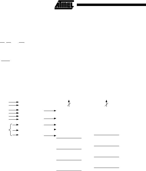
AT49BV/LV001NT pin 1 for the DIP and PLCC packages and pin 9 for the TSOP package are don’t connect pins.
To allow for simple in-system reprogrammability, the AT49BV/LV001(N)(T) does not require high input voltages for programming. Three-volt-only commands determine the read and programming operation of the device. Reading data out of the device is similar to reading from an EPROM; it has standard CE, OE, and WE inputs to avoid bus contention. Reprogramming the AT49BV/LV001(N)(T) is performed by erasing a block of data and then programming on a byte by byte basis. The byte programming time is a fast 50 μs. The end of a program cycle can be optionally detected by the DATA polling feature. Once the end of a byte program cycle has been detected, a new access for a read or program can begin. The typical number of program and erase cycles is in excess of 10,000 cycles.
The device is erased by executing the erase command sequence; the device internally controls the erase operations. There are two 8K byte parameter block sections and two main memory blocks.
The device has the capability to protect the data in the boot block; this feature is enabled by a command sequence. The 16K byte boot block section includes a reprogramming lock out feature to provide data integrity. The boot sector is designed to contain user secure code, and when the feature is enabled, the boot sector is protected from being reprogrammed.
In the AT49BV/LV001N(T), once the boot block programming lockout feature is enabled, the contents of the boot block are permanent and cannot be changed. In the AT49BV/LV001(T), once the boot block programming lockout feature is enabled, the contents of the boot block cannot be changed with input voltage levels of 5.5 volts or less.
Block Diagram
|
|
|
|
|
|
|
|
|
|
AT49BV/LV001(N) |
|
AT49BV/LV001(N)T |
|
|
|
|
|
|
|
|
|
|
DATA INPUTS/OUTPUTS |
|
DATA INPUTS/OUTPUTS |
|
|
|
|
|
|
|
|
|
|
|
|
I/O7 - I/O0 |
|
I/O7 - I/O0 |
|
|
VCC |
|
8 |
|
8 |
|
|||||||
|
GND |
|
|
|
|||||||||
|
|
|
|
|
|
|
|
||||||
|
|
|
|
|
|
|
|
|
|
INPUT/OUTPUT |
|
INPUT/OUTPUT |
|
|
|
OE |
|
|
|
|
|
||||||
|
|
|
|
|
BUFFERS |
|
BUFFERS |
|
|||||
|
|
|
|
|
|
|
CONTROL |
|
|
|
|
||
|
WE |
|
|
|
|
||||||||
|
|
|
|
|
|
|
|||||||
|
|
|
|
|
|
|
LOGIC |
|
|
|
|
|
|
|
|
|
CE |
|
|
PROGRAM |
|
PROGRAM |
|
||||
|
|
|
|
|
|
|
|
|
|
|
|
||
|
RESET |
|
|
|
|
DATA LATCHES |
|
DATA LATCHES |
|
||||
|
|
|
|
|
|
|
|
|
|
|
|
|
|
|
|
|
|
|
|
|
Y DECODER |
|
|
Y-GATING |
1FFFF |
Y-GATING |
1FFFF |
ADDRESS |
|
|
|
|
|
||||||||
|
|
|
MAIN MEMORY |
BOOT BLOCK |
|||||||||
|
|
|
|
|
|||||||||
INPUTS |
|
|
|
|
|
||||||||
X DECODER |
|
|
BLOCK 2 |
|
(16K BYTES) |
1C000 |
|||||||
|
|
|
|
|
|
|
|
|
|
||||
|
|
|
|
|
|
|
|
|
|
(64K BYTES) |
10000 |
|
|
|
|
|
|
|
|
|
|
|
|
PARAMETER |
1BFFF |
||
|
|
|
|
|
|
|
|
|
|
|
0FFFF |
||
|
|
|
|
|
|
|
|
|
|
MAIN MEMORY |
BLOCK 1 |
|
|
|
|
|
|
|
|
|
|
|
|
|
|
||
|
|
|
|
|
|
|
|
|
|
BLOCK 1 |
|
(8K BYTES) |
1A000 |
|
|
|
|
|
|
|
|
|
|
(32K BYTES) |
08000 |
|
|
|
|
|
|
|
|
|
|
|
|
PARAMETER |
19FFF |
||
|
|
|
|
|
|
|
|
|
|
|
07FFF |
||
|
|
|
|
|
|
|
|
|
|
|
|
||
|
|
|
|
|
|
|
|
|
|
PARAMETER |
BLOCK 2 |
|
|
|
|
|
|
|
|
|
|
|
|
|
|
||
|
|
|
|
|
|
|
|
|
|
BLOCK 2 |
|
(8K BYTES) |
18000 |
|
|
|
|
|
|
|
|
|
|
(8K BYTES) |
06000 |
|
|
|
|
|
|
|
|
|
|
|
|
MAIN MEMORY |
17FFF |
||
|
|
|
|
|
|
|
|
|
|
|
05FFF |
||
|
|
|
|
|
|
|
|
|
|
|
|
||
|
|
|
|
|
|
|
|
|
|
PARAMETER |
BLOCK 1 |
|
|
|
|
|
|
|
|
|
|
|
|
|
|
||
|
|
|
|
|
|
|
|
|
|
BLOCK 1 |
|
(32K BYTES) |
10000 |
|
|
|
|
|
|
|
|
|
|
(8K BYTES) |
04000 |
|
|
|
|
|
|
|
|
|
|
|
|
MAIN MEMORY |
0FFFF |
||
|
|
|
|
|
|
|
|
|
|
|
03FFF |
||
|
|
|
|
|
|
|
|
|
|
|
|
||
|
|
|
|
|
|
|
|
|
|
BOOT BLOCK |
BLOCK 2 |
|
|
|
|
|
|
|
|
|
|
|
|
|
|
||
|
|
|
|
|
|
|
|
|
|
(16K BYTES) |
00000 |
(64K BYTES) |
00000 |
|
|
|
|
|
|
|
|
|
|
|
|
||
|
|
|
|
|
|
|
|
|
|
|
|
||
2 AT49BV/LV001(N)(T) 

Device Operation
READ: The AT49BV/LV001(N)(T) is accessed like an EPROM. When CE and OE are low and WE is high, the data stored at the memory location determined by the address pins is asserted on the outputs. The outputs are put in the high impedance state whenever CE or OE is high. This dual-line control gives designers flexibility in preventing bus contention.
COMMAND SEQUENCES: When the device is first powered on it will be reset to the read or standby mode depending upon the state of the control line inputs. In order to perform other device functions, a series of command sequences are entered into the device. The command sequences are shown in the Command Definitions table. The command sequences are written by applying a low pulse on the WE or CE input with CE or WE low (respectively) and OE high. The address is latched on the falling edge of CE or WE, whichever occurs last. The data is latched by the first rising edge of CE or WE. Standard microprocessor write timings are used. The address locations used in the command sequences are not affected by entering the command sequences.
RESET: A RESET input pin is provided to ease some system applications. When RESET is at a logic high level, the device is in its standard operating mode. A low level on the RESET input halts the present device operation and puts the outputs of the device in a high impedance state. If the RESET pin makes a high to low transition during a program or erase operation, the operation may not be successfully completed and the operation will have to be repeated after a high level is applied to the RESET pin. When a high level is reasserted on the RESET pin, the device returns to the read or standby mode, depending upon the state of the control inputs. By applying a 12V ± 0.5V input signal to the RESET pin, the boot block array can be reprogrammed even if the boot block lockout feature has been enabled (see Boot Block Programming Lockout Override section). T h e R E S E T f e at u r e i s no t a v a i l ab l e o n t h e AT49BV/LV001N(T).
ERASURE: Before a byte can be reprogrammed, the main memory block or parameter block which contains the byte must be erased. The erased state of the memory bits is a logical “1”. The entire device can be erased at one time by using a 6 byte software code. The software chip erase code consists of 6 byte load commands to specific address locations with a specific data pattern (please refer to the Chip Erase Cycle Waveforms).
After the software chip erase has been initiated, the device will internally time the erase operation so that no external clocks are required. The maximum time needed to erase the whole chip is tEC. If the boot block lockout feature has been enabled, the data in the boot sector will not be erased.
AT49BV/LV001(N)(T)
CHIP ERASE: If the boot block lockout has been enabled, the Chip Erase function will erase Parameter Block 1, Parameter Block 2, Main Memory Block 1, and Main Memory Block 2 but not the boot block. If the Boot Block Lockout has not been enabled, the Chip Erase function will erase the entire chip. After the full chip erase the device will return back to read mode. Any command during chip erase will be ignored.
SECTOR ERASE: As an alternative to a full chip erase, the device is organized into sectors that can be individually erased. There are two 8K-byte parameter block sections and two main memory blocks. The 8K-byte parameter block sections can be independently erased and reprogrammed. The two main memory sections are designed to be used as alternative memory sectors. That is, whenever one of the blocks has been erased and reprogrammed, the other block should be erased and reprogrammed before the first block is again erased. The Sector Erase command is a six bus cycle operation. The sector address is latched on the falling WE edge of the sixth cycle while the 30H data input command is latched at the rising edge of WE. The sector erase starts after the rising edge of WE of the sixth cycle. The erase operation is internally controlled; it will automatically time to completion.
BYTE PROGRAMMING: Once the memory array is erased, the device is programmed (to a logical “0”) on a byte-by-byte basis. Please note that a data “0” cannot be programmed back to a “1”; only erase operations can convert “0”s to “1”s. Programming is accomplished via the internal device command register and is a 4 bus cycle operation (please refer to the Command Definitions table). The device will automatically generate the required internal program pulses.
The program cycle has addresses latched on the falling edge of WE or CE, whichever occurs last, and the data latched on the rising edge of WE or CE, whichever occurs first. Programming is completed after the specified tBP cycle
time. The DATA polling feature may also be used to indicate the end of a program cycle.
BOOT BLOCK PROGRAMMING LOCKOUT: The device has one designated block that has a programming lockout feature. This feature prevents programming of data in the designated block once the feature has been enabled. The size of the block is 16K bytes. This block, referred to as the boot block, can contain secure code that is used to bring up the system. Enabling the lockout feature will allow the boot code to stay in the device while data in the rest of the device is updated. This feature does not have to be activated; the boot block’s usage as a write protected region is optional to the user. The address range of the boot block is 00000 to 03FFF for the AT49BV/LV001(N) while the
3
address range of the boot block is 1C000 to 1FFFF for the AT49BV/LV001(N)T.
Once the feature is enabled, the data in the boot block can no longer be erased or programmed with input voltage level of 5.5V or less. Data in the main memory block can still be changed through the regular programming method. To activate the lockout feature, a series of six program commands to specific addresses with specific data must be performed. Please refer to the Command Definitions table.
BOOT BLOCK LOCKOUT DETECTION: A software method is available to determine if programming of the boot block section is locked out. When the device is in the software product identification mode (see Software Product Identification Entry and Exit sections) a read from address location 00002H will show if programming the boot block is locked out for the AT49BV/LV001(N) and a read from address 1C002H will show if programming the boot block is locked out for the AT49BV/LV001(N)T. If the data on I/O0 is low, the boot block can be programmed; if the data on I/O0 is high, the program lockout feature has been activated and the block cannot be programmed. The software product identification code should be used to return to standard operation.
BOOT BLOCK PROGRAMMING LOCKOUT OVERRIDE:
The user can override the boot block programming lockout by taking the RESET pin to 12 volts during the entire chip erase, sector erase or byte programming operation. When the RESET pin is brought back to TTL levels the boot block programming lockout feature is again active. This feature is not available on the AT49BV/LV001N(T).
PRODUCT IDENTIFICATION: The product identification mode identifies the device and manufacturer as Atmel. It
may be accessed by hardware or software operation. The hardware operation mode can be used by an external programmer to identify the correct programming algorithm for the Atmel product.
For details, see Operating Modes (for hardware operation) or Software Product Identification. The manufacturer and device code is the same for both modes.
DATA POLLING: The AT49BV/LV001(N)(T) features DATA polling to indicate the end of a program cycle. During a program cycle an attempted read of the last byte loaded will result in the complement of the loaded data on I/O7. Once the program cycle has been completed, true data is valid on all outputs and the next cycle may begin. DATA polling may begin at any time during the program cycle.
T O G G L E B I T : In a d di t i o n t o DA T A po l l i n g t h e AT49BV/LV001(N)(T) provides another method for determining the end of a program or erase cycle. During a program or erase operation, successive attempts to read data from the device will result in I/O6 toggling between one and zero. Once the program cycle has completed, I/O6 will stop toggling and valid data will be read. Examining the toggle bit may begin at any time during a program cycle.
HARDWARE DATA PROTECTION: Hardware features p r o te c t a ga i n s t i n ad v e r t en t p r o gr am s to t h e AT49BV/LV001(N)(T) in the following ways: (a) VCC sense: if VCC is below 1.8V (typical), the program function is inhib-
ited. (b) Program inhibit: holding any one of OE low, CE high or WE high inhibits program cycles. (c) Noise filter: pulses of less than 15 ns (typical) on the WE or CE inputs will not initiate a program cycle.
4 AT49BV/LV001(N)(T) 

 AT49BV/LV001(N)(T)
Command Definition (in Hex)(1)
|
|
1st Bus |
2nd Bus |
3rd Bus |
4th Bus |
5th Bus |
6th Bus |
||||||
Command |
Bus |
Cycle |
Cycle |
Cycle |
Cycle |
Cycle |
Cycle |
||||||
|
|
|
|
|
|
|
|
|
|
|
|
||
Sequence |
Cycles |
Addr |
Data |
Addr |
Data |
Addr |
Data |
Addr |
Data |
Addr |
Data |
Addr |
Data |
|
|
|
|
|
|
|
|
|
|
|
|
|
|
Read |
1 |
Addr |
DOUT |
|
|
|
|
|
|
|
|
|
|
Chip Erase |
6 |
5555 |
AA |
2AAA |
55 |
5555 |
80 |
5555 |
AA |
2AAA |
55 |
5555 |
10 |
|
|
|
|
|
|
|
|
|
|
|
|
|
|
Sector Erase |
6 |
5555 |
AA |
2AAA |
55 |
5555 |
80 |
5555 |
AA |
2AAA |
55 |
SA(4) |
30 |
Byte Program |
4 |
5555 |
AA |
2AAA |
55 |
5555 |
A0 |
Addr |
DIN |
|
|
|
|
Boot Block Lockout(2) |
6 |
5555 |
AA |
2AAA |
55 |
5555 |
80 |
5555 |
AA |
2AAA |
55 |
5555 |
40 |
Product ID Entry |
3 |
5555 |
AA |
2AAA |
55 |
5555 |
90 |
|
|
|
|
|
|
|
|
|
|
|
|
|
|
|
|
|
|
|
|
Product ID Exit(3) |
3 |
5555 |
AA |
2AAA |
55 |
5555 |
F0 |
|
|
|
|
|
|
Product ID Exit(3) |
1 |
XXXX |
F0 |
|
|
|
|
|
|
|
|
|
|
Notes: 1. The DATA FORMAT in each bus cycle is as follows: I/O7 - I/O0 (Hex)
2.The 16K byte boot sector has the address range 00000H to 03FFFH for the AT49BV/LV001(N) and 1C000H to 1FFFFH for the AT49BV/LV001(N)T.
3.Either one of the Product ID Exit commands can be used.
4.SA = sector addresses: For the AT49BV/LV001(N):
SA = 10000 to 1FFFF for BOOT BLOCK
Nothing will happen and the device goes back to the read mode in 100 ns SA = 04000 to 05FFF for PARAMETER BLOCK 1
SA = 06000 to 07FFF for PARAMETER BLOCK 2
SA = 08000 to 0FFFF for MAIN MEMORY ARRAY BLOCK 1 This command will erase - PB1, PB2 and MMB1
SA = 10000 to 1FFFF for MAIN MEMORY ARRAY BLOCK 2
For the AT49BV/LV001(N)T:
SA = 1C000 to 1FFFF for BOOT BLOCK
Nothing will happen and the device goes back to the read mode in 100 ns SA = 1A000 to 1BFFF for PARAMETER BLOCK 1
SA = 18000 to 19FFF for PARAMETER BLOCK 2
SA = 10000 to 17FFF for MAIN MEMORY ARRAY BLOCK 1 This command will erase - PB1, PB2 and MMB1
SA = 00000 to 0FFFF for MAIN MEMORY ARRAY BLOCK 2
Absolute Maximum Ratings*
Temperature Under Bias |
................................ -55°C to +125°C |
*NOTICE: Stresses beyond those listed under “Absolute Maxi- |
||
|
|
|
|
mum Ratings” may cause permanent damage to the |
Storage Temperature ..................................... |
-65°C to +150°C |
device. This is a stress rating only and functional |
||
|
|
|
|
operation of the device at these or any other condi- |
All Input Voltages |
|
tions beyond those indicated in the operational sec- |
||
(including NC Pins) |
|
tions of this specification is not implied. Exposure to |
||
with Respect to Ground ................................... |
-0.6V to +6.25V |
absolute maximum rating conditions for extended |
||
All Output Voltages |
|
periods may affect device reliability. |
||
|
|
|||
with Respect to Ground ............................. |
- 0.6V to VCC + 0.6V |
|
||
Voltage on |
|
|
|
|
OE |
|
|
||
with Respect to Ground ................................... |
-0.6V to +13.5V |
|
||
|
|
|
|
|
5

DC and AC Operating Range
|
|
AT49LV001(N)(T)-70 |
AT49BV/LV001(N)(T)-90 |
AT49BV/LV001(N)(T)-12 |
|
|
|
|
|
Operating |
Com. |
0°C - 70°C |
0°C - 70°C |
0°C - 70°C |
|
|
|
|
|
Temperature (Case) |
Ind. |
-40°C - 85°C |
-40°C - 85°C |
-40°C - 85°C |
|
||||
|
|
|
|
|
VCC Power Supply |
|
3.0V - 3.6V |
2.7V - 3.6V/3.0V - 3.6V |
2.7V - 3.6V/3.0V - 3.6V |
|
|
|
|
|
Operating Modes
Mode |
|
|
|
|
|
|
|
|
|
|
|
(6) |
|
|
Ai |
|
I/O |
||||
CE |
OE |
WE |
RESET |
|
|
||||||||||||||||
|
|
|
|
|
|
|
|
|
|
|
|
|
|
||||||||
Read |
|
VIL |
|
VIL |
|
VIH |
|
VIH |
|
|
Ai |
|
DOUT |
||||||||
Program/Erase(2) |
|
V |
|
V |
|
V |
IL |
|
V |
IH |
|
|
Ai |
|
D |
IN |
|||||
|
|
IL |
|
IH |
|
|
|
|
|
|
|
|
|
|
|||||||
Standby/Write Inhibit |
|
VIH |
|
X(1) |
|
X |
|
VIH |
|
|
X |
|
High Z |
||||||||
Program Inhibit |
|
X |
|
X |
|
VIH |
|
VIH |
|
|
|
|
|
|
|
||||||
Program Inhibit |
|
X |
|
VIL |
|
X |
|
VIH |
|
|
|
|
|
|
|
||||||
Output Disable |
|
X |
|
VIH |
|
X |
|
VIH |
|
|
|
|
|
High Z |
|||||||
Reset |
|
X |
|
X |
|
X |
|
VIL |
|
|
X |
|
High Z |
||||||||
Product Identification |
|
|
|
|
|
|
|
|
|
|
|
|
|
|
|
|
|
|
|
|
|
|
|
|
|
|
|
|
|
|
|
|
|
|
|
|
|
|
|
|
|
||
|
|
|
|
|
|
|
|
|
|
|
|
|
|
|
A1 - A16 = V |
IL |
, A9 = V ,(3) |
Manufacturer Code(4) |
|||
|
|
|
|
|
|
|
|
|
|
|
|
|
|
|
|
|
|
H |
|||
Hardware |
|
|
|
|
|
|
|
|
|
|
|
|
|
|
|
A0 = VIL |
|
|
|||
|
VIL |
|
VIL |
|
VIH |
|
|
|
|
A1 - A16 = V |
IL |
, A9 = V ,(3) |
Device Code(4) |
||||||||
|
|
|
|
|
|
|
|
||||||||||||||
|
|
|
|
|
|
|
|
|
|
|
|
|
|
|
|
|
|
H |
|||
|
|
|
|
|
|
|
|
|
|
|
|
|
|
|
|
A0 = VIH |
|
|
|||
Software(5) |
|
|
|
|
|
|
|
|
|
|
|
|
|
|
A0 = VIL, A1 - A16=VIL |
Manufacturer Code(4) |
|||||
|
|
|
|
|
|
|
|
|
|
|
|
|
|
A0 = V |
IH |
, A1 - A16=V |
Device Code(4) |
||||
|
|
|
|
|
|
|
|
|
|
|
|
|
|
|
|||||||
|
|
|
|
|
|
|
|
|
|
|
|
|
|
|
|
|
|
IL |
|
|
|
Notes: 1. X can be VIL or VIH.
2.Refer to AC Programming Waveforms.
3.VH = 12.0V ± 0.5V.
4.Manufacturer Code: 1FH, Device Code: 05H - AT49BV/LV001(N), 04H - AT49BV/LV001(N)T.
5.See details under Software Product Identification Entry/Exit.
6.This pin is not available on the AT49BV/LV001N(T).
DC Characteristics
Symbol |
|
Parameter |
|
Condition |
Min |
Max |
Units |
||
|
|
|
|
|
|
|
|
||
ILI |
|
Input Load Current |
|
VIN = 0V to VCC |
|
10 |
μA |
||
ILO |
|
Output Leakage Current |
|
VI/O = 0V to VCC |
|
10 |
μA |
||
ISB1 |
|
VCC Standby Current CMOS |
|
|
|
= VCC - 0.3V to VCC |
|
50 |
μA |
|
CE |
|
|||||||
ISB2 |
|
VCC Standby Current TTL |
|
|
= 2.0V to VCC |
|
3 |
mA |
|
|
CE |
|
|||||||
(1) |
|
VCC Active Current |
|
f = 5 MHz; IOUT = 0 mA |
|
25 |
mA |
||
ICC |
|
|
|
||||||
VIL |
|
Input Low Voltage |
|
|
|
|
|
0.6 |
V |
VIH |
|
Input High Voltage |
|
|
|
|
2.0 |
|
V |
VOL |
|
Output Low Voltage |
IOL = 2.1 mA |
|
.45 |
V |
|||
VOH |
|
Output High Voltage |
IOH = -400 μA |
2.4 |
|
V |
|||
Note: |
1. In the erase mode, ICC is 50 mA. |
|
|
|
|
|
|
|
|
6 AT49BV/LV001(N)(T) 
 Loading...