


ATMEL AT28BV16-30TI, AT28BV16-30TC, AT28BV16-30SI, AT28BV16-30SC, AT28BV16-30PI Datasheet
...
 AT28BV16
Features
∙ 2.7 to 3.6V Supply
Full Read and Write Operation ∙ Low Power Dissipation
8 mA Active Current
μ
∙Read Access Time - 250 ns
∙Byte Write - 3 ms
∙Direct Microprocessor Control DATA Polling
READ/BUSY Open Drain Output on TSOP
∙High Reliability CMOS Technology Endurance: 100,000 Cycles Data Retention: 10 Years
∙Low Voltage CMOS Compatible Inputs and Outputs
∙JEDEC Approved Byte Wide Pinout
∙Commercial and Industrial Temperature Ranges50 A CMOS Standby Current
Description
The AT28BV16 is a low-power, high-performance Electrically Erasable and Programmable Read Only Memory with easy to use features. The AT28BV16 is a 16K memory organized as 2,048 words by 8 bits. The device is manufactured with Atmel’s reliable nonvolatile CMOS technology.
The AT28BV16 is accessed like a static RAM for the read or write cycles without the need of external components. During a byte write, the address and data are latched
(continued)
Pin Configurations
|
Pin Name |
Function |
|
|
|
|
|
|
|
|
|
||
|
A0 - A10 |
Addresses |
|
|
|
|
|
|
|
TSOP |
|
||
|
|
|
|
|
|
|
|
Top View |
|
||||
|
|
|
|
|
|
|
|
|
|
|
|
|
|
|
CE |
Chip Enable |
|
|
|
|
|
|
|
|
|
||
|
OE |
Output Enable |
|
|
|
|
|
|
|
|
|
||
|
|
|
|
|
|
|
|
|
|
||||
|
|
|
|
|
|
|
|
|
|
|
|
||
|
|
|
|
|
|
|
|
|
|
|
|
|
|
|
WE |
Write Enable |
|
|
|
|
|
|
|
|
|
||
|
|
|
|
|
|
|
|
|
|
||||
|
|
|
|
|
|
|
|
|
|
||||
|
|
|
|
|
|
|
|
|
|
||||
|
|
|
|
|
|
|
|
|
|
|
|
|
|
|
I/O0 - I/O7 |
Data Inputs/Outputs |
|
|
|
|
|
|
|
|
|
||
|
|
|
|
|
|
|
|
|
|
||||
|
|
|
|
|
|
|
|
|
|
||||
|
|
|
|
|
|
|
|
|
|
||||
|
|
|
|
|
|
|
|
|
|
||||
|
|
|
|
|
|
|
|
|
|
|
|
|
|
|
NC |
No Connect |
|
|
|
|
|
|
|
|
|
||
|
|
|
|
|
|
|
|
|
|
||||
|
|
|
|
|
|
|
|
|
|
||||
|
|
|
|
|
|
|
|
|
|
||||
|
|
|
|
|
|
|
|
|
|
||||
|
|
|
|
|
|
|
|
|
|
|
|
|
|
|
DC |
Don’t Connect |
|
|
|
|
|
|
|
|
|
||
|
|
|
|
|
|
|
|
|
|
||||
|
|
|
|
|
|
|
|
|
|
||||
|
|
|
|
|
|
|
|
|
|
||||
|
|
|
|
|
|
|
|
|
|
||||
|
|
|
|
|
|
|
|
|
|
||||
|
|
|
|
|
|
|
|
|
|
|
|
|
|
|
PDIP, SOIC |
|
|
|
|
|
|
|
|
|
PLCC |
|
|||||||||||||
|
Top View |
|
|
|
|
|
|
|
|
Top View |
|
||||||||||||||
|
|
|
|
|
|
|
|
|
|
|
|
|
|
|
|
|
|
|
|
|
|
|
|
|
|
|
|
|
|
|
|
|
|
|
|
|
|
|
|
|
|
|
|
|
|
|
|
|
|
|
|
|
|
|
|
|
|
|
|
|
|
|
|
|
|
|
|
|
|
|
|
|
|
|
|
|
|
|
|
|
|
|
|
|
|
|
|
|
|
|
|
|
|
|
|
|
|
|
|
|
|
|
|
|
|
|
|
|
|
|
|
|
|
|
|
|
|
|
|
|
|
|
|
|
|
|
|
|
|
|
|
|
|
|
|
|
|
|
|
|
|
|
|
|
|
|
|
|
|
|
|
|
|
|
|
|
|
|
|
|
|
|
|
|
|
|
|
|
|
|
|
|
|
|
|
|
|
|
|
|
|
|
|
|
|
|
|
|
|
|
|
|
|
|
|
|
|
|
|
|
|
|
|
|
|
|
|
|
|
|
|
|
|
|
|
|
|
|
|
|
|
|
|
|
|
|
|
|
|
|
|
|
|
|
|
|
|
|
|
|
|
|
|
|
|
|
|
|
|
|
|
|
|
|
|
|
|
|
|
|
|
|
|
|
|
|
|
|
|
|
|
|
|
|
|
|
|
|
|
|
|
|
|
|
|
|
|
|
|
|
|
|
|
|
|
|
|
|
|
|
|
|
|
|
|
|
|
|
|
|
|
|
|
|
|
|
|
|
|
|
|
|
|
|
|
|
|
|
|
|
|
|
|
|
|
|
|
|
|
|
|
|
|
|
|
|
|
|
|
|
|
|
|
|
|
|
|
|
|
|
|
|
|
|
|
|
|
|
|
|
|
|
|
|
|
|
|
|
|
|
|
|
|
|
|
|
|
|
|
|
|
|
|
|
|
|
|
|
|
|
|
|
|
|
|
|
|
|
|
|
|
|
|
|
|
|
|
|
|
|
|
|
|
|
|
|
|
|
|
|
|
|
|
|
|
|
|
|
|
|
|
|
|
|
|
|
|
|
|
|
|
|
|
|
|
|
|
|
|
|
|
|
|
|
|
|
|
|
|
|
|
|
|
|
|
|
|
|
|
|
|
|
|
|
|
|
|
|
|
|
|
|
|
|
|
|
|
|
|
|
|
|
|
|
|
|
|
|
|
|
|
|
|
|
|
|
|
|
|
|
|
|
|
|
|
|
|
|
|
|
|
|
|
|
|
|
|
|
|
|
|
|
|
|
|
|
|
|
|
|
|
|
|
|
|
|
|
|
|
|
|
|
|
|
|
|
|
|
|
|
|
|
|
|
|
|
|
|
|
|
|
|
|
|
|
|
|
|
|
|
|
|
|
|
|
|
|
|
|
|
|
|
|
|
|
|
|
|
|
|
|
|
|
|
|
|
|
|
|
|
|
|
|
|
|
|
|
|
|
|
|
|
|
|
|
|
|
|
|
|
|
|
|
|
|
|
|
|
|
|
|
|
|
|
|
|
|
|
|
|
|
|
|
|
|
|
|
|
|
|
|
|
|
|
|
|
|
|
|
|
|
|
|
|
|
|
|
|
|
|
|
|
|
|
|
|
|
|
|
|
|
|
|
|
|
|
|
|
|
|
|
|
|
|
|
|
|
|
|
|
|
|
|
|
|
|
|
16K (2K x 8)
Battery-Voltage™
CMOS E2PROM
0308A
2-119
Description (Continued)
internally, freeing the microprocessor address and data bus for other operations. Following the initiation of a write cycle, the device will go to a busy state and automatically clear and write the latched data using an internal control timer. The end of a write cycle can be determined by DATA polling of I/O7. Once the end of a write cycle has been detected, a new access for a read or a write can begin.
The CMOS technology offers fast access times of 250 ns at low power dissipation. When the chip is deselected the standby current is less than 50 μA.
Atmel’s 28BV16 has additional features to ensure high quality and manufacturability. The device utilizes error correction internally for extended endurance and for improved data retention characteristics. An extra 32-bytes of E2PROM are available for device identification or tracking.
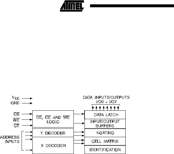
Block Diagram
Absolute Maximum Ratings*
Temperature Under Bias |
................. -55°C to +125°C |
||
Storage Temperature...................... |
-65°C to +150°C |
||
All Input Voltages |
|
||
(including NC Pins) |
|
||
with Respect to Ground ................... |
-0.6V to +6.25V |
||
All Output Voltages |
|
||
with Respect to Ground ............. |
- 0.6V to VCC + 0.6V |
||
|
|
|
|
Voltage on OE and A9 |
|
||
with Respect to Ground ................... |
-0.6V to +13.5V |
||
|
|
|
|
*NOTICE: Stresses beyond those listed under “Absolute Maximum Ratings” may cause permanent damage to the device. This is a stress rating only and functional operation of the device at these or any other conditions beyond those indicated in the operational sections of this specification is not implied. Exposure to absolute maximum rating conditions for extended periods may affect device reliability.
2-120 AT28BV16 

Device Operation
READ: The AT28BV16 is accessed like a Static RAM. When CE and OE are low and WE is high, the data stored at the memory location determined by the address pins is asserted on the outputs. The outputs are put in a high impedance state whenever CE or OE is high. This dual line control gives designers increased flexibility in preventing bus contention.
BYTE WRITE: Writing data into the AT28BV16 is similar to writing into a Static RAM. A low pulse on the WE or CE input with OE high and CE or WE low (respectively) initiates a byte write. The address location is latched on the last falling edge of WE (or CE); the new data is latched on the first rising edge. Internally, the device performs a selfclear before write. Once a byte write has been started, it will automatically time itself to completion. Once a programming operation has been initiated and for the duration of tWC, a read operation will effectively be a polling operation.
DATA POLLING: The AT28BV16 provides DATA POLLING to signal the completion of a write cycle. During a write cycle, an attempted read of the data being written results in the complement of that data for I/O7 (the other outputs are indeterminate). When the write cycle is finished, true data appears on all outputs.
AT28BV16
READY/BUSY (TSOP only): READY/BUSY is an open drain output; it is pulled low during the internal write cycle and released at the completion of the write cycle.
WRITE PROTECTION: Inadvertent writes to the device are protected against in the following ways. (a) Vcc sense— if Vcc is below 2.0V (typical) the write function is inhibited. (b) Vcc power on delay— once Vcc has reached 2.0V the device will automatically time out 5 ms (typical) before allowing a byte write. (c) Write Inhibit— holding any one of OE low, CE high or WE high inhibits byte write cycles.
DEVICE IDENTIFICATION: An extra 32-bytes of E2PROM memory are available to the user for device identification. By raising A9 to 12 ± 0.5V and using address locations 7E0H to 7FFH the additional bytes may be written to or read from in the same manner as the regular memory array.
2-121
 Loading...