


ATMEL AT27C520-90XI, AT27C520-90XC, AT27C520-90TI, AT27C520-90TC, AT27C520-90SI Datasheet
...
Features
•8-Bit Multiplexed Addresses/Outputs
•Fast Read Access Time - 70 ns
•Low Power CMOS Operation
–20 mA max. Active at 5 MHz
•20-Lead TSSOP Package
•20-Lead SOIC Package
•28-Lead TSOP Package
•5V ± 10% Supply
•High Reliability CMOS Technology
–2,000V ESD Protection
–200 mA Latchup Immunity
• Rapid™ Programming Algorithm - 50 μs/byte (typical)
•CMOS and TTL Compatible Inputs and Outputs
•Integrated Product Identification Code
•Commercial and Industrial Temperature Range
Description
The AT27C520 is a low-power, high performance 524,288 bit one-time programmable read only memory (OTP EPROM) organized 64K by 8 bits. It incorporates latches for the 8 lower order address bits to multiplex with the 8 data bits. This minimizes system chip count, reduces cost, and simplifies the design of multiplexed bus systems. It requires only one 5V power supply in normal read mode operation. Any byte can be accessed in less than 70 ns, eliminating the need for speed reducing WAIT states on high performance microprocessor systems.
Atmel’s scaled CMOS technology provides high speed, lower active power consumption, and significantly faster programming. Power consumption is typically only 8 mA in Active Mode.
The AT27C520 is available in 173 mil, 20-pin TSSOP; 300 mil, 20-pin SOIC; and 28pin TSOP, one-time programmable (OTP) plastic packages.
(continued)
Pin Configurations |
|
|
|
|
TSSOP Top View |
|||||||||||||||||
|
Pin Name |
Function |
|
|
|
|
A10 |
|
|
1 |
|
|
20 |
|
A8 |
|||||||
|
|
|
|
|
|
|
|
|
||||||||||||||
|
|
|
|
|
|
|
|
|
||||||||||||||
|
|
|
|
|
|
|
|
|
|
|
|
A12 |
|
|
2 |
|
|
19 |
|
AD1 |
||
|
A8 - A15 |
Addresses |
|
|
|
|||||||||||||||||
|
|
|
|
|
A14 |
|
|
3 |
|
|
18 |
|
AD3 |
|||||||||
|
|
|
|
|
|
|
|
|
||||||||||||||
|
|
|
|
|
|
|
|
|
||||||||||||||
|
|
|
|
|
|
|
|
|
|
|
|
ALE |
|
|
4 |
|
|
17 |
|
AD5 |
||
|
AD0 - AD7 |
Addresses/Outputs |
|
|
|
|||||||||||||||||
|
|
|
|
|
VCC |
|
|
5 |
|
|
16 |
|
AD7 |
|||||||||
|
|
|
|
|
|
|
|
|
||||||||||||||
|
|
|
|
|
|
|
|
|
||||||||||||||
|
|
|
|
|
|
|
|
|
|
|
OE/VPP |
|
|
|
6 |
|
|
15 |
|
GND |
||
|
|
|
|
|
|
|
|
|
|
|
|
|
|
|||||||||
|
|
|
|
|
|
|
|
|
|
|
||||||||||||
|
OE /VPP |
Output Enable/VPP |
|
|
|
|
A15 |
|
|
7 |
|
|
14 |
|
AD6 |
|||||||
|
|
|
|
|
A13 |
|
|
|
|
8 |
|
|
13 |
|
AD4 |
|||||||
|
|
|
|
|
|
|
|
|
|
|
|
|
|
|
|
|
||||||
|
ALE |
|
Address Latch Enable |
|
|
|
||||||||||||||||
|
|
|
|
|
|
A11 |
|
|
9 |
|
|
12 |
|
AD2 |
||||||||
|
|
|
|
|
|
|
|
|
|
|||||||||||||
|
|
|
|
|
|
A9 |
|
|
|
|
10 |
|
11 |
|
AD0 |
|||||||
|
|
|
|
|
|
|
|
|
|
|
|
|
|
|
|
|||||||
|
|
|
|
TSOP Top View |
|
|
||||||||||||||||
|
|
|
|
|
|
|
|
|
|
|
|
|
|
|
|
|
|
|
||||
|
|
|
|
|
|
|
|
|
|
|
|
|
|
|
|
|
|
|
||||
|
|
|
|
|
|
|
|
|
|
|
|
|
SOIC Top View |
|||||||||
|
A10 |
22 |
21 |
|
A8 |
|
|
|
|
|||||||||||||
|
|
|
|
|
|
|
|
|
|
|
|
|
|
|
|
|||||||
|
NC |
23 |
20 |
|
NC |
|
|
|
|
|
|
|
|
|
|
|
|
|
|
|||
|
NC |
24 |
19 |
|
NC |
|
|
|
|
|
|
|
|
|
|
|
|
|
|
|||
|
OE/VPP |
|
|
|
1 |
|
|
20 |
|
VCC |
||||||||||||
|
A12 |
25 |
18 |
|
AD1 |
|
|
|
A15 |
|
|
|
2 |
|
|
19 |
|
ALE |
||||
|
A14 |
26 |
17 |
|
AD3 |
|
|
|
|
|
|
|
|
|
||||||||
|
|
|
|
|
A13 |
|
|
|
3 |
|
|
18 |
|
A14 |
||||||||
|
ALE |
27 |
16 |
|
AD5 |
|
|
|
|
|
|
|
|
|
||||||||
|
|
|
|
|
A11 |
|
|
|
4 |
|
|
17 |
|
A12 |
||||||||
|
VCC |
28 |
15 |
|
AD7 |
|
|
|
|
|
|
|
|
|
||||||||
|
|
|
|
|
A9 |
|
|
|
5 |
|
|
16 |
|
A10 |
||||||||
OE/VPP |
1 |
14 |
|
GND |
|
|
|
|
|
|
|
|
|
|||||||||
|
|
|
|
AD0 |
|
|
|
6 |
|
|
15 |
|
A8 |
|||||||||
|
A15 |
2 |
13 |
|
AD6 |
|
|
|
|
|
|
|
|
|
||||||||
|
|
|
|
|
AD2 |
|
|
|
7 |
|
|
14 |
|
AD1 |
||||||||
|
A13 |
3 |
12 |
|
AD4 |
|
|
|
|
|
|
|
|
|
||||||||
|
|
|
|
|
|
|||||||||||||||||
|
A11 |
4 |
11 |
|
AD2 |
|
|
|
AD4 |
|
|
|
8 |
|
|
13 |
|
AD3 |
||||
|
|
|
|
|
|
|
||||||||||||||||
|
|
|
|
|
|
|||||||||||||||||
|
NC |
5 |
10 |
|
NC |
|
|
|
AD6 |
|
|
|
9 |
|
|
12 |
|
AD5 |
||||
|
|
|
|
|
|
|||||||||||||||||
|
NC |
6 |
9 |
|
NC |
|
|
|
GND |
|
|
|
10 |
|
11 |
|
AD7 |
|||||
|
|
|
|
|
||||||||||||||||||
|
A9 |
7 |
8 |
|
AD0 |
|
|
|
|
|
|
|
|
|
|
|
|
|
|
|||
|
|
|
|
|
|
|
|
|
|
|
|
|
|
|
|
|
|
|
|
|
|
|
|
|
|
|
|
|
|
|
|
|
|
|
|
|
|
|
|
|
|
|
|
|
|
|
|
|
|
|
|
|
|
|
|
|
|
|
|
|
|
|
|
|
|
|
|
|
|
|
|
|
|
|
|
|
|
|
|
|
|
|
|
|
|
|
|
|
|
|
|
|
|
|
|
|
|
|
|
|
|
|
|
|
|
|
|
|
|
|
|
|
|
|
512K (64K x 8) Multiplexed Addresses/ Outputs
OTP EPROM
AT27C520
Rev. 0752C-C–01/98
1
With 64K byte storage capability, the AT27C520 allows firmware to be stored reliably and to be accessed by the system without the delays of mass storage media.
Atmel's 27C520 has additional features to ensure high quality and efficient production use. The Rapid™ Programming Algorithm reduces the time required to program the part and guarantees reliable programming. Programming time is typically only 50 μs/byte. The Integrated Product Identification Code electronically identifies the device and manufacturer. This feature is used by industry standard programming equipment to select the proper programming algorithms and voltages.
System Considerations
Switching under active conditions may produce transient voltage excursions. Unless accommodated by the system design, these transients may exceed data sheet limits, resulting in device non-conformance. At a minimum, a 0.1 μF high frequency, low inherent inductance, ceramic capacitor should be utilized for each device. This capacitor should be connected between the VCC and Ground terminals of the device, as close to the device as possible. Additionally, to stabilize the supply voltage level on printed circuit boards with large EPROM arrays, a 4.7 μF bulk electrolytic capacitor should be utilized, again connected between the VCC and Ground terminals. This capacitor should be positioned as close as possible to the point where the power supply is connected to the array.
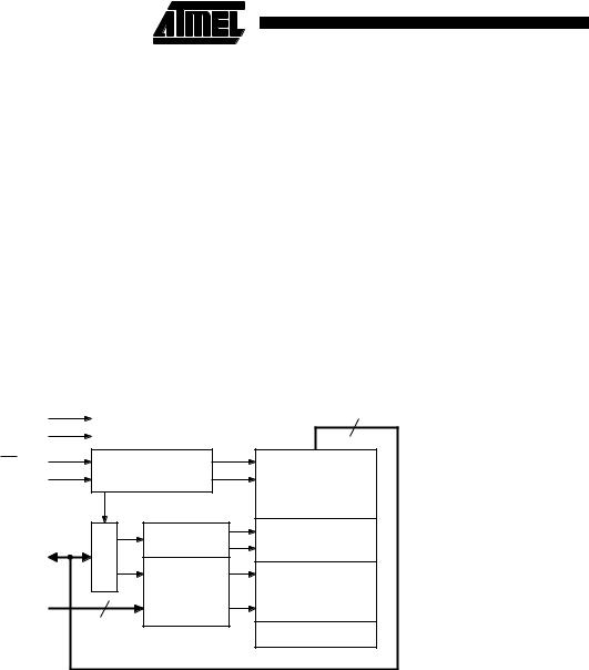
Block Diagram
VCC |
|
|
8 |
|
GND |
|
|
|
|
OE/VPP |
|
OE, ALE, AND |
OUTPUT |
|
ALE |
PROGRAM LOGIC |
|||
BUFFERS |
||||
|
|
|
||
|
LATCHES |
Y DECODER |
Y-GATING |
|
AD7 - AD0 |
|
|
||
|
X DECODER |
CELL MATRIX |
||
|
8 |
|||
A15 - A8 |
|
|
||
|
|
|
||
|
|
|
IDENTIFICATION |
|
2 |
AT27C520 |
|
|
||
|

Absolute Maximum Ratings*
Temperature Under Bias |
................................ -55°C to +125°C |
Storage Temperature ..................................... |
-65°C to +150°C |
Voltage on Any Pin with |
-2.0V to +7.0V(1) |
Respect to Ground ......................................... |
|
Voltage on A9 with |
-2.0V to +14.0V(1) |
Respect to Ground ...................................... |
|
VPP Supply Voltage with |
-2.0V to +14.0V(1) |
Respect to Ground ....................................... |
|
|
|
AT27C520
*NOTICE: Stresses beyond those listed under “Absolute Maximum Ratings” may cause permanent damage to the device. This is a stress rating only and functional operation of the device at these or any other conditions beyond those indicated in the operational sections of this specification is not implied. Exposure to absolute maximum rating conditions for extended periods may affect device reliability.
Note: 1. Minimum voltage is -0.6V DC which may undershoot to -2.0V for pulses of less than 20 ns. Maximum output pin voltage is VCC + 0.75V DC which may overshoot to +7.0V for pulses of less than 20 ns.
Operating Modes
|
|
|
|
|
|
|
|
|
|
Mode/Pin |
ALE |
OE/VPP |
A8 - A15 |
|
AD0 - AD7 |
||||
Read |
VIL |
|
VIL |
Ai |
|
DOUT |
|||
Output Disable |
V /V |
|
V |
IH |
X(1) |
|
High Z/A0 - A7 |
||
|
IL IH |
|
|
|
|
|
|
|
|
Address Latch Enable |
VIH |
|
VIH |
X |
|
A0 - A7 |
|||
Rapid Program(2) |
V |
|
V |
|
Ai |
|
D |
IN |
|
|
IH |
|
|
PP |
|
|
|
||
Product Identification(3) |
|
|
|
|
|
A9 = VH(4) |
|
|
|
V |
|
V |
IL |
A8 = V or V |
IL |
Identification Code |
|||
|
IL |
|
|
|
IH |
|
|
||
|
|
|
|
|
|
A10 - A15 = VIL |
|
|
|
Notes: 1. X can be VIL or VIH. |
|
|
|
|
|
|
|
|
|
2.Refer to Programming Characteristics.
3.VH = 12.0 ± 0.5V.
4.Two identifier bytes may be selected. All A8 - A15 inputs are held low (VIL), except A9 which is set to VH and A8 which is toggled low (VIL) to select the Manufacturer’s Identification byte and high (VIH) to select the Device Code byte.
3
 Loading...