


ATMEL AT22LV10-25PI, AT22LV10-25JI, AT22LV10-20SI, AT22LV10-20SC, AT22LV10-20PI Datasheet
...
Features
•Low Voltage Programmable Logic Device
–Wide Power Supply Range - 3.0V to 5.5V
–Ideal for Battery Powered Systems
•High Speed Operation
–20 ns max Propagation Delay at V CC = 3.0V
•Commercial and Industrial Temperature Ranges
•Familiar 22V10 Logic Architecture
•Low Power 3-Volt CMOS Operation
|
AT22LV10L |
AT22LV10 |
|
|
|
|
|
Temp |
Com./Ind. |
Com./Ind. |
|
|
|
|
VCC = 3.6V |
ICC (mA) |
4 / 5 |
35 / 45 |
•CMOS and TTL Compatible Inputs and Outputs
–10 μA Leakage Maximum
•Reprogrammable - Tested 100% for Programmability
•High Reliability CMOS Technology
–2000V ESD Protection
–200 mA Latchup Immunity
•Dual-In-Line and Surface Mount Packages
Logic Diagram
Description
The AT22LV10 and AT22LV10L are low voltage compatible CMOS high performance Programmable Logic Devices (PLDs). Speeds down to 20 ns and power dissipation as low as 14.4 mW are offered. All speed ranges are specified over the 3.0V to 5.5V range. All pins offer a low ±10 μA leakage.
(continued)
Pin Configurations |
DIP/SOIC |
PLCC |
|
Pin Name |
Function |
|
|
CLK/IN |
Clock and Logic Input |
|
|
IN |
Logic Inputs |
|
|
I/O |
Bidirectional Buffers |
|
|
* |
No Internal Connection |
|
|
VCC |
3.0V to 5.5V Supply |
|
|
Low-Voltage UV |
Erasable |
Programmable |
Logic Device |
AT22LV10 |
AT22LV10L |
Rev. 0190C—05/98 |
1 |
The AT22LV10L provides the optimum low power CMOS PLD solution, with low DC power (1 mA typical at VCC = 3.3V) and full CMOS output levels. The AT22LV10L significantly reduces total system power, allowing battery powered operation.
Full CMOS output levels help reduce power in many other system components.
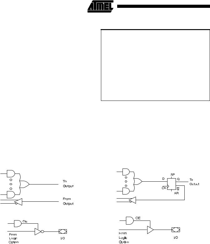
The AT22LV10 and AT22LV10L logic architectures are identical to the familiar 22V10. Each output is allocated from eight to 16 product terms, which allows highly complex logic functions to be realized.
Two additional product terms are included to provide synchronous preset and asynchronous reset. These terms are common to all ten registers. All registers are automatically cleared upon power up.
Register preload simplifies testing. A security fuse prevents unauthorized copying of programmed fuse patterns.
Absolute Maximum Ratings*
Temperature Under Bias ................................ |
-55°C to +125°C |
Storage Temperature ..................................... |
-65°C to +150°C |
Voltage on Any Pin with |
-2.0V to +7.0V (1) |
Respect to Ground........................................ |
|
Voltage on Input Pins |
|
with Respect to Ground |
-2.0V to +14.0V (1) |
During Programming................................... |
|
Programming Voltage with |
-2.0V to +14.0V (1) |
Respect to Ground...................................... |
|
Integrated UV Erase Dose ............................. |
7258 W•sec/cm2 |
*NOTICE: Stresses beyond those listed under “Absolute Maximum Ratings” may cause permanent damage to the device. This is a stress rating only and functional operation of the device at these or any other conditions beyond those indicated in the operational sections of this specification is not implied. Exposure to absolute maximum rating conditions for extended periods may affect device reliability.
Note: 1. Minimum voltage is -0.6V dc whihc may undershoot to -2.0V for pulses of less than 20 ns. Maximum pin voltage is VCC + 0.75V dc which may undershoot to VCC + 2.0V for pulses of less than 20 ns.
Logic Options
Output Options
DC and AC Operating Conditions
|
Commercial |
Industrial |
|
|
|
Operating Temperature (Case) |
0°C - 70°C |
-40°C - 85°C |
|
|
|
VCC Power Supply |
3.0V to 5.5V |
3.0V to 5.5V |
|
|
|
2 AT22LV10(L) 

AT22LV10(L)
DC Characteristics
Symbol |
Parameter |
Condition |
|
|
Min |
Typ |
Max |
Units |
|
|
|
|
|
|
|
|
|
ILI |
Input Load Current |
VIN = -0.1V to VCC + 1V |
|
|
|
10 |
μA |
|
ILO |
Output Leakage |
VOUT = -0.1V to VCC + 0.1V |
|
|
|
10 |
μA |
|
Current |
|
|
|
|||||
|
|
|
|
|
|
|
|
|
|
|
|
|
|
|
|
|
|
|
|
|
AT22LV10 |
Com. |
|
20/50 |
35/90 |
mA |
|
|
VCC = 3.6V / 5.5V, |
|
|
|
|
|
|
ICC |
Power Supply |
Ind. |
|
20/50 |
45/100 |
mA |
||
|
|
|||||||
VIN = GND, |
|
|
|
|
|
|
||
Current |
|
Com. |
|
1/2 |
4/12 |
mA |
||
|
Outputs Open |
|
|
|||||
|
|
AT22LV10L |
|
|||||
|
|
|
Ind. |
|
1/2 |
5/15 |
mA |
|
|
|
|
|
|
||||
|
|
|
|
|
|
|
|
|
(1) |
Output Short Circuit |
VOUT = 0.5V |
|
|
|
|
-120 |
mA |
IOS |
Current |
|
|
|
|
|||
|
|
|
|
|
|
|
|
|
|
|
|
|
|
|
|
|
|
VIL1 |
Input Low Voltage |
4.5V ≤ VCC ≤ 5.5V |
|
|
-0.6 |
|
0.8 |
V |
VIL2 |
Input Low Voltage |
3.0V ≤ VCC < 4.5V |
|
|
-0.6 |
|
0.6 |
V |
VIH |
Input High Voltage |
|
|
|
2.0 |
|
VCC + 0.75 |
V |
|
Output Low Voltage |
VCC = 3.0V |
Com.,Ind. |
IOL = 8 mA |
|
|
0.5 |
V |
|
|
|
|
|
|
|
|
|
VOL |
VCC = 4.5V |
Com.,Ind. |
IOL = 16 mA |
|
|
0.5 |
V |
|
VIN = VIH or VIL |
|
|
||||||
|
VCC = 3.0V |
Com.,Ind. |
IOL = 6 mA |
|
|
0.35 |
V |
|
|
|
|
|
|||||
VOH |
Output High Voltage |
VIN = VIH or VIL, |
IOH = -100 μA |
|
VCC - 0.3 |
|
|
V |
VCC = 3.0V / 4.5V |
IOH = -0.4 mA / -4.0 mA |
2.4 |
|
|
V |
|||
|
|
|
|
|||||
Note: 1. |
Not more than one output at a time should be shorted. Duration of short circuit test should not exceed 30 sec. |
|
||||||
3
AC Characteristics for the AT22LV10
|
|
|
AT22LV10-20 |
|
|
AT22LV10-25 |
|
|
||||
|
|
|
|
|
|
|
|
|
|
|
|
|
Symbol |
Parameter |
Min |
|
Typ |
|
Max |
Min |
|
Typ |
|
Max |
Units |
|
|
|
|
|
|
|
|
|
|
|
|
|
tPD |
Input or Feedback to Non- |
|
|
12 |
|
20 |
|
|
15 |
|
25 |
ns |
Registered Output |
|
|
|
|
|
|
||||||
|
|
|
|
|
|
|
|
|
|
|
|
|
|
|
|
|
|
|
|
|
|
|
|
|
|
tEA |
Input to Output Enable |
|
|
|
|
20 |
|
|
15 |
|
25 |
ns |
tER |
Input to Output Disable |
|
|
|
|
20 |
|
|
15 |
|
25 |
ns |
tCF |
Clock to Feedback |
0 |
|
4 |
|
9 |
0 |
|
5 |
|
9 |
ns |
tCO |
Clock to Output |
0 |
|
8 |
|
14 |
0 |
|
10 |
|
17 |
ns |
tS |
Input or Feedback Setup Time |
10 |
|
6 |
|
|
12 |
|
7 |
|
|
ns |
tH |
Hold Time |
0 |
|
|
|
|
0 |
|
|
|
|
ns |
|
|
|
|
|
|
|
|
|
|
|
|
|
tP |
Clock Period |
10 |
|
|
|
|
12 |
|
|
|
|
ns |
|
|
|
|
|
|
|
|
|
|
|
|
|
tW |
Clock Width |
5 |
|
|
|
|
6 |
|
|
|
|
ns |
|
External Feedback 1/(tS+tCO) |
|
|
|
|
41.6 |
|
|
|
|
34.5 |
MHz |
FMAX |
|
|
|
|
|
|
|
|
|
|
|
|
Internal Feedback 1/(tS + tCF) |
|
|
|
|
52.6 |
|
|
|
|
47.6 |
MHz |
|
|
No Feedback 1/(tP) |
|
|
|
|
100.0 |
|
|
|
|
83.3 |
MHz |
|
|
|
|
|
|
|
|
|
|
|
|
|
tAW |
Asynchronous Reset Width |
20 |
|
12 |
|
|
25 |
|
15 |
|
|
ns |
|
Asynchronous Reset, |
|
|
|
|
|
|
|
|
|
|
|
tAR |
Synchronous Preset, |
20 |
|
12 |
|
|
25 |
|
15 |
|
|
ns |
|
Recovery Time |
|
|
|
|
|
|
|
|
|
|
|
|
|
|
|
|
|
|
|
|
|
|
|
|
tAP |
Asynchronous Reset to |
|
|
15 |
|
25 |
|
|
18 |
|
28 |
ns |
Registered Output Reset |
|
|
|
|
|
|
||||||
|
|
|
|
|
|
|
|
|
|
|
|
|
|
|
|
|
|
|
|
|
|
|
|
|
|
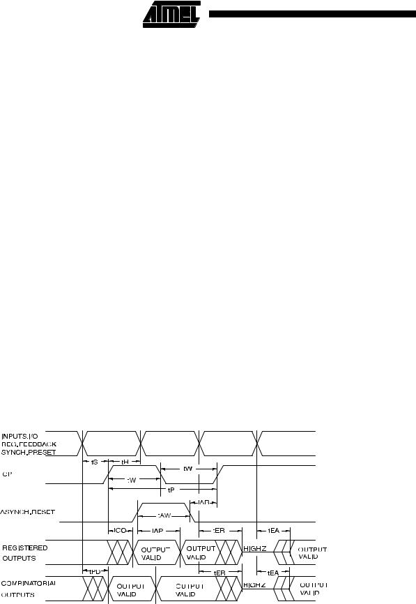
AC Waveforms(1)
Note: 1. Timing measurement reference is 1.5V. Input AC driving levels are 0.0V and 3.0V, unless otherwise specified.
4 AT22LV10(L) 
 Loading...