


ATMEL AT28HC256F-12LM-883, AT28HC256E-12LM-883, AT28HC256F-90LM-883, AT28HC256E-90LM-883, AT28HC256E-12SI Datasheet
...
Features
•Fast Read Access Time - 70 ns
•Automatic Page Write Operation
–Internal Address and Data Latches for 64 Bytes
–Internal Control Timer
•Fast Write Cycle Times
–Page Write Cycle Time: 3 ms or 10 ms Maximum
–1 to 64-Byte Page Write Operation
•Low Power Dissipation
–80 mA Active Current
–3 mA Standby Current
•Hardware and Software Data Protection
•DATA Polling for End of Write Detection
•High Reliability CMOS Technology
–Endurance: 10 4 or 105 Cycles
–Data Retention: 10 Years
•Single 5V ± 10% Supply
•CMOS and TTL Compatible Inputs and Outputs
•JEDEC Approved Byte-Wide Pinout
•Full Military, Commercial, and Industrial Temperature Ranges
Description
The AT28HC256 is a high-performance Electrically Erasable and Programmable Read Only Memory. Its 256K of memory is organized as 32,768 words by 8 bits. Manufactured with Atmel’s advanced nonvolatile CMOS technology, the AT28HC256
(continued)
Pin Configurations
|
Pin Name |
Function |
|||
|
|
|
|||
|
A0 - A14 |
Addresses |
|||
|
|
|
|
|
|
|
|
|
|
|
Chip Enable |
|
CE |
||||
|
|
|
|
|
|
|
|
|
|
|
Output Enable |
|
OE |
||||
|
|
|
|
||
|
|
|
|
|
Write Enable |
|
WE |
||||
|
|
|
|||
|
I/O0 - I/O7 |
Data Inputs/Outputs |
|||
|
|
|
|||
|
NC |
No Connect |
|||
|
|
|
|||
|
DC |
Don’t Connect |
|||
|
|
|
|
|
|
TSOP
Top View
|
|
|
|
|
|
|
|
|
|
|
|
|
|
|
|
|
|
|
|
|
OE |
1 |
28 |
|
A10 |
||||
A11 |
2 |
27 |
|
|
|
||||
|
CE |
||||||||
|
|
A9 |
3 |
26 |
|
I/O7 |
|||
|
|
A8 |
4 |
25 |
|
I/O6 |
|||
A13 |
5 |
24 |
|
I/O5 |
|||||
|
|
|
6 |
23 |
|
I/O4 |
|||
|
WE |
|
|||||||
VCC |
7 |
22 |
|
I/O3 |
|||||
A14 |
8 |
21 |
|
GND |
|||||
A12 |
9 |
20 |
|
I/O2 |
|||||
|
|
A7 |
10 |
19 |
|
I/O1 |
|||
|
|
A6 |
11 |
18 |
|
I/O0 |
|||
|
|
A5 |
12 |
17 |
|
A0 |
|||
|
|
A4 |
13 |
16 |
|
A1 |
|||
|
|
A3 |
14 |
15 |
|
A2 |
|||
|
|
|
|
|
|
|
|
|
|
|
LCC, PLCC |
|
|
|
|
CERDIP, PDIP, FLATPACK |
PGA |
|
|
|
||||||||||||||||||||||
|
|
Top View |
|
|
|
|
|
|
Top View |
|
|
|
|
|
|
|
|
|
Top View |
|
|
|
||||||||||
|
A7 |
A12 |
A14 |
DC |
VCC |
|
WE |
A13 |
|
|
|
|
|
|
|
|
|
|
|
|
|
|
|
|
|
|
|
|
|
|
|
|
|
|
|
|
|
A14 |
|
1 |
28 |
|
|
VCC |
|
|
|
|
|
|
|
|
|
|
|
||||||||||
|
|
|
|
|
|
|
|
|
|
|
|
A12 |
|
2 |
27 |
|
|
|
|
|
|
|
|
|
|
|
|
|
|
|
|
|
|
4 |
3 |
2 |
1 |
32 |
31 |
30 |
|
|
|
|
|
|
WE |
|
|
|
|
|
|
|
|
|
|
|
|||||||
|
|
|
|
A7 |
|
3 |
26 |
|
|
A13 |
|
|
|
|
|
|
|
|
|
|
|
|||||||||||
A6 |
5 |
|
|
|
|
|
|
29 |
A8 |
|
|
|
|
|
|
|
|
|
|
|
|
|
|
|||||||||
A5 |
6 |
|
|
|
|
|
|
28 |
A9 |
A6 |
|
4 |
25 |
|
|
A8 |
|
|
|
|
|
|
|
|
|
|
|
|||||
|
|
|
|
|
|
|
|
|
|
|
|
|
|
|
|
|
|
|
||||||||||||||
A4 |
7 |
|
|
|
|
|
|
27 |
A11 |
A5 |
|
5 |
24 |
|
|
A9 |
|
|
|
|
|
|
|
|
|
|
|
|||||
|
|
|
|
|
|
|
|
|
|
|
|
|
|
|
|
|
|
|
||||||||||||||
|
|
|
|
|
|
|
|
|
|
|
|
|
|
|
|
|
|
|
||||||||||||||
A3 |
8 |
|
|
|
|
|
|
26 |
NC |
A4 |
|
6 |
23 |
|
|
A11 |
|
|
|
|
|
|
|
|
|
|
|
|||||
|
|
|
|
|
|
|
|
|
|
|
|
|
|
|
|
|
|
|
||||||||||||||
A2 |
9 |
|
|
|
|
|
|
25 |
|
|
|
A3 |
|
7 |
22 |
|
|
|
OE |
|
|
|
|
|
|
|
|
|
|
|
||
|
|
|
|
|
|
OE |
|
|
|
|
|
|
|
|
||||||||||||||||||
|
|
|
|
|
|
|
|
|
|
|
|
|
|
|
|
|
|
|
|
|||||||||||||
A1 |
10 |
|
|
|
|
|
|
24 |
A10 |
A2 |
|
8 |
21 |
|
|
A10 |
|
|
|
|
|
|
|
|
|
|
||||||
|
|
|
|
|
|
|
|
|
|
|
|
|
|
|||||||||||||||||||
|
|
|
|
|
|
|
|
|
|
|
|
|
|
|
|
|
|
|
||||||||||||||
A0 |
11 |
|
|
|
|
|
|
23 |
|
|
A1 |
|
9 |
20 |
|
|
|
CE |
|
|
|
|
|
|
|
|
|
|
|
|||
|
|
|
|
|
|
CE |
|
|
|
|
|
|
|
|
|
|
|
|
|
|||||||||||||
|
|
|
|
|
|
|
|
|
|
|
|
|
|
|
|
|
|
|
|
|
||||||||||||
NC |
12 |
|
|
|
|
|
|
22 |
I/O7 |
A0 |
|
10 |
19 |
|
|
I/O7 |
|
|
|
|
|
|
|
|
|
|
|
|||||
I/O0 |
13 |
|
|
|
|
|
|
21 |
I/O6 |
I/O0 |
|
11 |
18 |
|
|
I/O6 |
|
|
|
|
|
|
|
|
|
|
|
|||||
|
|
|
|
|
|
|
|
|
|
|
|
|
|
|
|
|
|
|
||||||||||||||
|
14 |
15 |
16 |
17 |
18 |
19 |
20 |
|
|
|
I/O1 |
|
12 |
17 |
|
|
I/O5 |
|
|
|
|
|
|
|
|
|
|
|
||||
|
|
|
|
|
|
|
|
|
|
|
|
|
|
|
|
|
|
|||||||||||||||
|
I/O1 |
I/O2 |
GND |
DC |
I/O3 |
|
I/O4 |
I/O5 |
|
|
|
I/O2 |
|
13 |
16 |
|
|
I/O4 |
|
|
|
|
|
|
|
|
|
|
|
|||
|
|
|
|
|
GND |
|
14 |
15 |
|
|
I/O3 |
|
|
|
|
|
|
|
|
|||||||||||||
|
|
|
|
|
|
|
|
|
|
|
|
|
|
|
|
|
|
|
|
|
|
|
||||||||||
|
|
|
|
|
|
|
|
|
|
|
|
|
|
|
|
|
|
|
|
|
|
|
|
|
|
|
|
|
|
|
|
|
Note: PLCC package pins 1 and 17 are DON’T CONNECT.
256 (32K x 8) |
High Speed |
Parallel |
EEPROMs |
AT28HC256 |
Rev. 0007G–10/98 |
1 |
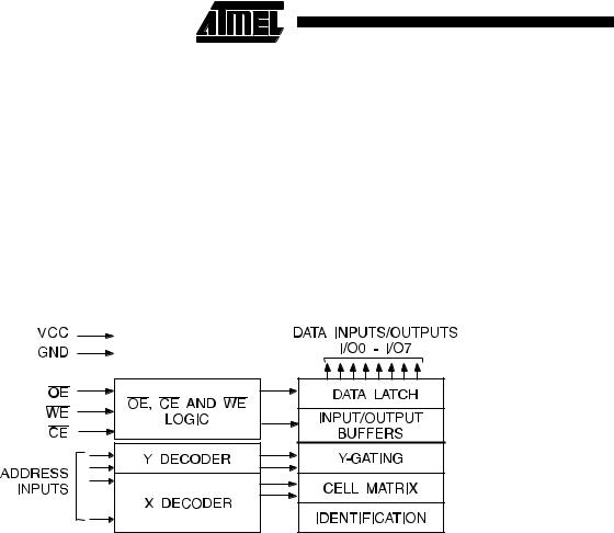
offers access times to 70 ns with power dissipation of just 440 mW. When the AT28HC256 is deselected, the standby current is less than 5 mA.
The AT28HC256 is accessed like a Static RAM for the read or write cycle without the need for external components. The device contains a 64-byte page register to allow writing of up to 64 bytes simultaneously. During a write cycle, the address and 1 to 64 bytes of data are internally latched, freeing the addresses and data bus for other operations. Following the initiation of a write cycle, the device will automatically write the latched data using an internal control timer. The end of a write cycle can be detected by DATA
polling of I/O7. Once the end of a write cycle has been detected a new access for a read or write can begin.
Atmel’s 28HC256 has additional features to ensure high quality and manufacturability. The device utilizes internal error correction for extended endurance and improved data retention characteristics. An optional software data protection mechanism is available to guard against inadvertent writes. The device also includes an extra 64 bytes of EEPROM for device identification or tracking.
Block Diagram
Absolute Maximum Ratings*
Temperature Under Bias |
................................ -55°C to +125°C |
*NOTICE: Stresses beyond those listed under “Absolute |
||
|
|
|
|
Maximum Ratings” may cause permanent dam- |
Storage Temperature ..................................... |
-65°C to +150°C |
age to the device. This is a stress rating only and |
||
|
|
|
|
functional operation of the device at these or any |
All Input Voltages |
|
other conditions beyond those indicated in the |
||
(including NC Pins) |
|
operational sections of this specification is not |
||
with Respect to Ground ................................... |
-0.6V to +6.25V |
implied. Exposure to absolute maximum rating |
||
All Output Voltages |
|
conditions for extended periods may affect |
||
- 0.6V to VCC + 0.6V |
device reliability |
|||
with Respect to Ground ............................. |
|
|||
Voltage on |
|
and A9 |
|
|
OE |
|
|
||
with Respect to Ground ................................... |
-0.6V to +13.5V |
|
||
|
|
|
|
|
2 |
AT28HC256 |
|
|
||
|
Device Operation
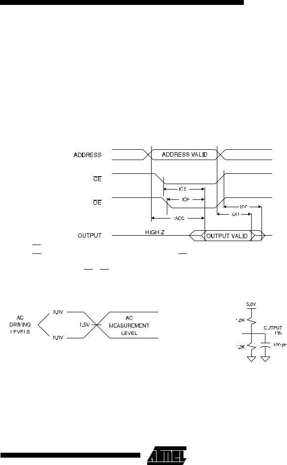
READ: The AT28HC256 is accessed like a Static RAM. When CE and OE are low and WE is high, the data stored at the memory location determined by the address pins is asserted on the outputs. The outputs are put in the high impedance state when either CE or OE is high. This dualline control gives designers flexibility in preventing bus contention in their system.
BYTE WRITE: A low pulse on the WE or CE input with CE or WE low (respectively) and OE high initiates a write cycle. The address is latched on the falling edge of CE or WE, whichever occurs last. The data is latched by the first rising edge of CE or WE. Once a byte write has been started it will automatically time itself to completion. Once a programming operation has been initiated and for the duration of tWC, a read operation will effectively be a polling operation.
P A G E W R I T E : Th e pa ge w r it e op er a ti on o f th e AT28HC256 allows 1 to 64 bytes of data to be written into the device during a single internal programming period. A page write operation is initiated in the same manner as a byte write; the first byte written can then be followed by 1 to 63 additional bytes. Each successive byte must be written
within 150 μs (tBLC) of the previous byte. If the tBLC limit is exceeded the AT28C256 will cease accepting data and
commence the internal programming operation. All bytes during a page write operation must reside on the same page as defined by the state of the A6 - A14 inputs. That is, for each WE high to low transition during the page write operation, A6 - A14 must be the same.
The A0 to A5 inputs are used to specify which bytes within the page are to be written. The bytes may be loaded in any order and may be altered within the same load period. Only bytes which are specified for writing will be written; unnecessary cycling of other bytes within the page does not occur.
DATA POLLING: The AT28HC256 features DATA Polling to indicate the end of a write cycle. During a byte or page write cycle an attempted read of the last byte written will result in the complement of the written data to be presented on I/O7. Once the write cycle has been completed, true data is valid on all outputs, and the next write cycle may begin. DATA Polling may begin at anytime during the write cycle.
TOGGLE BIT: In addition to DATA Polling the AT28HC256 provides another method for determining the end of a write cycle. During the write operation, successive attempts to read data from the device will result in I/O6 toggling between one and zero. Once the write has completed, I/O6 will stop toggling and valid data will be read. Testing the toggle bit may begin at any time during the write cycle.
DATA PROTECTION: If precautions are not taken, inadvertent writes to any 5-volt-only nonvolatile memory may
AT28HC256
occur during transition of the host system power supply. Atmel has incorporated both hardware and software features that will protect the memory against inadvertent writes.
HARDWARE PROTECTION: Hardware features protect against inadvertent writes to the AT28HC256 in the following ways: (a) VCC sense—if V CC is below 3.8V (typical) the write function is inhibited; (b) VCC power-on delay—once VCC has reached 3.8V the device will automatically time out 5 ms typical) before allowing a write; (c) write inhibit—hold- ing any one of OE low, CE high or WE high inhibits write cycles; and (d) noise filter—pulses of less than 15 ns (typical) on the WE or CE inputs will not initiate a write cycle.
SOFTWARE DATA PROTECTION: A software controlled data protection feature has been implemented on the AT28HC256. When enabled, the software data protection (SDP), will prevent inadvertent writes. The SDP feature may be enabled or disabled by the user; the AT28HC256 is shipped from Atmel with SDP disabled.
SDP is enabled by the host system issuing a series of three write commands; three specific bytes of data are written to three specific addresses (refer to Software Data Protection Algorithm). After writing the 3-byte command sequence and after tWC the entire AT28HC256 will be protected against inadvertent write operations. It should be noted, that once protected the host may still perform a byte or page write to the AT28HC256. This is done by preceding the data to be written by the same 3-byte command sequence.
Once set, SDP will remain active unless the disable command sequence is issued. Power transitions do not disable SDP and SDP will protect the AT28HC256 during power-up and power-down conditions. All command sequences must conform to the page write timing specifications. It should also be noted that the data in the enable and disable command sequences is not written to the device and the memory addresses used in the sequence may be written with data in either a byte or page write operation.
After setting SDP, any attempt to write to the device without the three byte command sequence will start the internal write timers. No data will be written to the device; however, for the duration of tWC, read operations will effectively be polling operations.
DEVICE IDENTIFICATION: An extra 64 bytes of EEPROM memory are available to the user for device identification. By raising A9 to 12V ± 0.5V and using address locations 7FC0H to 7FFFH the additional bytes may be written to or read from in the same manner as the regular memory array.
OPTIONAL CHIP ERASE MODE: The entire device can be erased using a 6-byte software code. Please see Software Chip Erase application note for details.
3

DC and AC Operating Range
|
|
AT28HC256-70 |
AT28HC256-90 |
AT28HC256-12 |
|
|
|
|
|
|
|
|
Com. |
0°C - 70°C |
0°C - 70°C |
0°C - 70°C |
|
Operating |
|
|
|
|
|
Ind. |
-40°C - 85°C |
-40°C - 85°C |
-40°C - 85°C |
||
Temperature (Case) |
|||||
|
|
|
|
||
Mil. |
|
-55°C - 125°C |
-55°C - 125°C |
||
|
|
||||
|
|
|
|
|
|
VCC Power Supply |
|
5V ± 10% |
5V ± 10% |
5V ± 10% |
Operating Modes
|
|
|
|
|
|
|
|
|
|
|
|
|
|
Mode |
CE |
|
OE |
|
WE |
I/O |
|||||||
|
|
|
|
|
|
|
|
|
|
|
|||
Read |
|
VIL |
|
VIL |
|
VIH |
DOUT |
||||||
Write(2) |
|
V |
IL |
|
V |
IH |
|
V |
IL |
D |
|||
|
|
|
|
|
|
|
IN |
||||||
Standby/Write Inhibit |
|
V |
|
|
|
X(1) |
|
X |
High Z |
||||
|
|
IH |
|
|
|
|
|
|
|
|
|
||
Write Inhibit |
|
X |
|
X |
|
VIH |
|
||||||
Write Inhibit |
|
X |
|
VIL |
|
X |
|
||||||
Output Disable |
|
X |
|
VIH |
|
X |
High Z |
||||||
Chip Erase |
|
V |
IL |
V |
(3) |
|
V |
IL |
High Z |
||||
|
|
|
|
H |
|
|
|
||||||
Notes: 1. X can be VIL or VIH.
2.Refer to AC Programming Waveforms.
3.VH = 12.0V ± 0.5V.
DC Characteristics
Symbol |
Parameter |
|
Condition |
|
|
Min |
Max |
Units |
|
|
|
|
|
|
|
|
|||
ILI |
Input Load Current |
|
VIN = 0V to VCC + 1V |
|
10 |
μA |
|||
ILO |
Output Leakage Current |
VI/O = 0V to VCC |
|
|
|
10 |
μA |
||
ISB1 |
VCC Standby Current TTL |
|
|
= 2.0V to VCC |
+ 1V |
AT28HC256-90, -12 |
|
3 |
mA |
|
CE |
|
|
|
|
||||
|
AT28HC256-70 |
|
60 |
mA |
|||||
|
|
|
|
|
|
|
|||
|
|
|
|
|
|
|
|
|
|
ISB2 |
VCC Standby Current CMOS |
|
|
= -3.0V to VCC + 1V |
AT28HC256-90, -12 |
|
300 |
μA |
|
CE |
|
||||||||
ICC |
VCC Active Current |
|
f = 5 MHz; IOUT = 0 mA |
|
80 |
mA |
|||
VIL |
Input Low Voltage |
|
|
|
|
|
|
0.8 |
V |
VIH |
Input High Voltage |
|
|
|
|
|
2.0 |
|
V |
VOL |
Output Low Voltage |
IOL = 6.0 mA |
|
|
|
0.45 |
V |
||
VOH |
Output High Voltage |
|
IOH = -4 mA |
|
|
2.4 |
|
V |
|
4 |
AT28HC256 |
|
|
||
|
AT28HC256
AC Read Characteristics
|
|
|
|
|
|
|
|
|
|
|
AT28HC256-70 |
AT28C256-90 |
AT28HC256-12 |
|
||||
|
|
|
|
|
|
|
|
|
|
|
|
|
|
|||||
Symbol |
|
|
|
|
|
Parameter |
Min |
Max |
Min |
Max |
Min |
Max |
Units |
|||||
|
|
|
|
|
|
|
|
|
|
|||||||||
tACC |
|
Address to Output Delay |
|
70 |
|
90 |
|
120 |
ns |
|||||||||
(1) |
|
|
|
|
|
|
|
|
|
|
|
|
|
|
|
|
|
|
CE to Output Delay |
|
70 |
|
90 |
|
120 |
ns |
|||||||||||
tCE |
|
|
|
|
||||||||||||||
(2) |
|
|
|
|
|
|
|
|
|
|
|
|
|
|
|
|
|
|
OE to Output Delay |
0 |
35 |
0 |
40 |
0 |
50 |
ns |
|||||||||||
tOE |
|
|||||||||||||||||
tDF(3)(4) |
|
|
or |
|
to Output Float |
0 |
35 |
0 |
40 |
0 |
50 |
ns |
||||||
CE |
OE |
|||||||||||||||||
|
|
Output Hold from |
|
|
|
or Address, |
|
|
|
|
|
|
|
|||||
tOH |
|
OE, |
CE |
0 |
|
0 |
|
0 |
|
ns |
||||||||
|
whichever occurred first |
|
|
|
||||||||||||||
|
|
|
|
|
|
|
|
|
||||||||||
|
|
|
|
|
|
|
|
|
|
|
|
|
|
|
|
|
|
|
AC Read Waveforms(1)(2)(3)(4)
Notes: 1. CE may be delayed up to tACC - tCE after the address transition without impact on tACC.
2.OE may be delayed up to tCE - tOE after the falling edge of CE without impact on tCE or by tACC - tOE after an address change without impact on tACC.
3.tDF is specified from OE or CE whichever occurs first (CL = 5 pF).
4.This parameter is characterized and is not 100% tested.
Input Test Waveforms and |
Output Test Load |
Measurement Level |
|
tR, tF < 5 ns
Pin Capacitance
f = 1 MHz, T = 25°C (1)
Symbol |
|
Typ |
Max |
Units |
Conditions |
|
|
|
|
|
|
CIN |
|
4 |
6 |
pF |
VIN = 0V |
COUT |
|
8 |
12 |
pF |
VOUT = 0V |
Note: 1. |
This parameter is characterized and is not 100% tested. |
|
|
||
5
 Loading...