


T5760 / T5761
UHF ASK/FSK Receiver
Description
The T5760/T5761 is a multi-chip PLL receiver device supplied in an SO20 package. It has been especially developed for the demands of RF low-cost data transmission systems with data rates from 1 kBaud to 10 kBaud in Manchester or Bi-phase code. The receiver is well suited to operate with the Atmel Wireless & Microcontrollers’ PLL RF transmitter T5750. Its main applications are in
the areas of telemetering, security technology and key- less-entry systems. It can be used in the frequency receiving range of f0 = 868 to 870 MHz or f0 = 902 to 928 MHz for ASK or FSK data transmission. All the statements made below refer to 868.3 MHz and 915.0 MHz applications.
Features
DFully integrated LC-VCO and PLL loop filter
DVery high sensitivity with power matched LNA
D30 dB image rejection
DHigh system IIP3 (–16 dBm), system 1-dB compression point (–25 dBm)
DHigh large-signal capability at GSM band (blocking –30 dBm @ + 20 MHz, IIP3 = –12 dBm @ + 20 MHz)
D5 V to 20 V automotive compatible data interface
DData clock available for Manchesterand Bi-phase- coded signals
DProgrammable digital noise suppresion
DReceiving bandwidth BIF = 600 kHz for low cost 90-ppm crystals
DLow power consumption due to configurable polling
DTemperature range –40° C to 105° C
DESD protection 2 kV HBM, 200 V MM
DCommunication to mC possible via a single bi-directional data line
DLow-cost solution due to high integration level with minimum external circuitry requirements
System Block Diagram
UHF ASK/FSK |
UHF ASK/FSK |
Remote control transmitter |
Remote control receiver |
T5750 |
|
T5760/ |
|
|
|
|
|
T5761 |
Demod. |
Control |
1...5 |
|
|
|
|
mC |
|
XTO |
PLL |
|
|
|
|
|
Antenna |
Antenna |
IF Amp |
|
|
|
|
|
|
||
|
VCO |
|
PLL |
XTO |
|
|
|
|
|
||
|
Power |
LNA |
VCO |
|
|
|
amp. |
|
|
||
|
|
|
|
|
Figure 1. System block diagram
Ordering Information
Extended Type Number |
Package |
Remarks |
|
|
|
T5760-TG |
SO20 |
Tube, for 868 MHz ISM band |
T5760-TGQ |
SO20 |
Taped and reeled, for 868 MHz ISM band |
T5761-TG |
SO20 |
Tube, for 915 MHz ISM band |
T5761-TGQ |
SO20 |
Taped and reeled, for 915 MHz ISM band |
|
|
|
Rev. A2, 19-Oct-00 |
1 (32) |
Preliminary Information

T5760 / T5761
Pin Description
Pin |
Symbol |
Function |
1 |
SENS |
Sensitivity-control resistor |
|
|
|
2 |
IC_ |
IC condition indicator |
|
ACTIVE |
Low = sleep mode |
|
|
High = active mode |
|
|
|
3 |
CDEM |
Lower cut-off frequency data fil- |
|
|
ter |
|
|
|
4 |
AVCC |
Analog power supply |
|
|
|
5 |
TEST 1 |
Test pin, during operation at GND |
|
|
|
6 |
AGND |
Analog ground |
|
|
|
7 |
n.c. |
Not connected, connect to GND |
|
|
|
8 |
LNAREF |
High-frequency reference node |
|
|
LNA and mixer |
|
|
|
9 |
LNA_IN |
RF input |
|
|
|
10 |
LNAGND |
DC ground LNA and mixer |
|
|
|
11 |
TEST 2 |
Do not connect during operating |
|
|
|
12 |
TEST 3 |
Test pin, during operation at GND |
|
|
|
13 |
n.c. |
Not connected, connect to GND |
|
|
|
14 |
XTAL |
Crystal oscillator XTAL connec- |
|
|
tion |
|
|
|
15 |
DVCC |
Digital power supply |
|
|
|
16 |
TEST 4 |
Test pin, during operation at |
|
|
DVCC |
|
|
|
17 |
DATA_ |
Bit clock of data stream |
|
CLK |
|
|
|
|
18 |
DGND |
Digital ground |
|
|
|
19 |
POLL- |
Selects polling or rceiving mode |
|
ING/_ON |
Low: receiving mode |
|
|
High: polling mode |
|
|
|
20 |
DATA |
Data output / configuration input |
|
|
|
|
|
|
|
|
|
SENS |
1 |
|
|
20 |
DATA |
|
|
|
|
|
|
|
|
|
|
|
|
IC_ACTIVE |
2 |
|
|
19 |
POLLING |
|
|
|
|
|
/_ON |
|
|
|
|
|
|
CDEM |
3 |
|
|
18 |
DGND |
|
|
|
|
|
DATA_CLK |
AVCC |
4 |
|
|
17 |
|
|
|
|
|
|
|
TEST 1 |
5 |
|
16 |
TEST 4 |
|
|
|
|
T5760/ |
|
|
AGND |
6 |
|
T5761 |
15 |
DVCC |
|
|
||||
|
|
|
|
|
|
n.c. |
7 |
|
|
14 |
XTAL |
|
|
|
|
|
|
LNAREF |
8 |
|
|
13 |
n.c. |
LNA_IN |
|
|
|
|
TEST 3 |
9 |
|
|
12 |
||
|
|
|
|
|
TEST 2 |
|
|
|
|
|
|
LNAGND |
10 |
|
|
11 |
|
|
|
|
|
|
|
Figure 2. Pinning SO20
2 (32) |
Rev. A2, 19-Oct-00 |
Preliminary Information
T5760 / T5761
Block Diagram
|
FSK/ASK– |
Dem_out |
Data – |
|
CDEM |
demodulator |
|
interface |
|
|
and data filter |
|
|
|
|
Rssi |
Limiter out |
|
|
|
RSSI IF |
|
|
|
SENS |
Amp. |
Sensitivity– |
|
|
|
Polling circuit |
|||
|
|
reduction |
||
AVCC |
|
and |
|
|
|
|
|
||
AGND |
|
|
control logic |
|
4. Order |
|
|
|
|
DGND |
f0=950 kHz/ |
|
|
|
1 MHz |
|
FE |
CLK |
|
DVCC |
|
|
|
|
|
LPF |
|
|
|
|
fg=2.2MHz |
|
Standby logic |
|
|
|
|
|
|
IF |
|
|
|
Loop– |
|
Amp. |
|
|
|
|
filter |
|
|
|
Poly–LPF |
|
|
fg=7MHz |
LC–VCO |
XTO |
LNAREF |
|
f |
f |
LNA_IN LNA |
:256 |
:2 |
LNAGND
DATA
POLLING/_ON
DATA_CLK
 IC_ACTIVE
XTAL
Figure 3. Block diagram
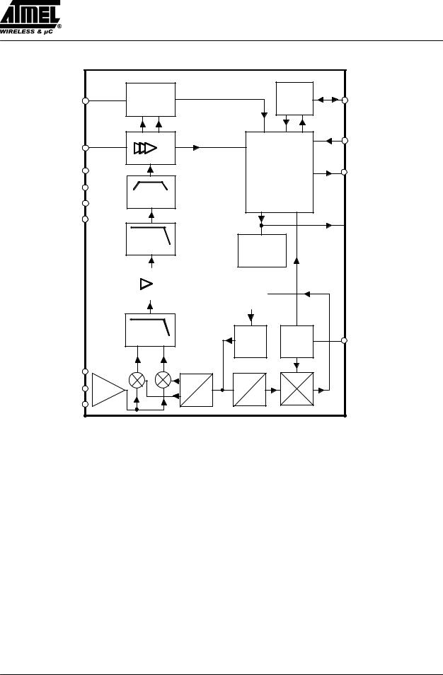
RF Front End
The RF front end of the receiver is a low-IF heterodyne configuration that converts the input signal into a 950-kHz/ 1-MHz IF signal with an image rejection of typical 30dB. According to figure 3 the front end consists of an LNA (low noise amplifier), LO (local oscillator), I/Q mixer, polyphase lowpass filter and an IF amplifier.
The PLL generates the carrier frequency for the mixer via a full integrated synthesizer with integrated low noise LC-VCO (voltage controlled oscillator ) and PLL-loop- filter. The XTO ( crystal oscillator ) generates the
reference frequency fXTO. The integrated LC-VCO generates two times the mixer drive frequency fVCO. The I/Q
signals for the mixer are generated with a divide by two
circuit ( fLO = fVCO/2 ). fVCO is divided by a factor of 256 and feed into a phase frequency detector and compared
with fXTO. The output of the phase frequency detector is feed into an integrated loopfilter and thereby generates the control voltage for the VCO. If fLO is determined, fXTO can be calculated using the following formula:
fXTO = fLO / 128
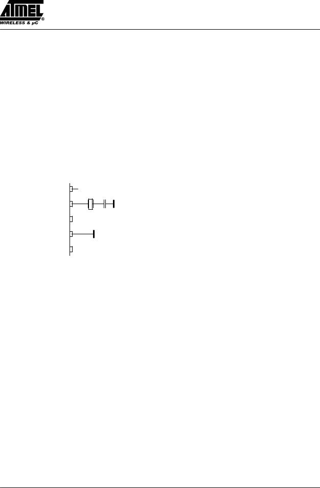
The XTO is a one-pin oscillator that operates at the series resonance of the quartz crystal with high current but low voltage signal, so that there is only a small voltage at the crystal oscillator frequency at Pin XTAL. According to figure 4, the crystal should be connected to GND with a series capacitor CL. The value of that capacitor is recommended by the crystal supplier. Due to a somewhat inductive impedance at steady state oscillation and some PCB parasitics a lower value of CL is normally necessary.
Rev. A2, 19-Oct-00 |
3 (32) |
Preliminary Information
T5760 / T5761
The value of CL should be optimized for the individual board layout to achieve the exact value of fXTO (the best way is to use a crystal with known load resonance frequency to find the right value for this capacitor) and hereby of fLO. When designing the system in terms of receiving bandwidth and local oscillator accuracy, the accuracy of the crystal and the XTO must be considered.
If a crystal with $30 ppm adjustment tolerance at 25_C , $50ppm over Temperature –40_C to 105_C, $10 ppm of total aging and a CM ( motional capacitance ) of 7 fF is used, an additional XTO pulling of $30 ppm has to be added.
The resulting total LO tolerance of $120ppm agrees with the receiving bandwidth specification of the T5760/T5761 if the T5750 has also a total LO tolerance of $120 ppm.
V
S
DVCC
CL
XTAL
n.c.
TEST 3
TEST 2
Figure 4. XTO peripherals
The nominal frequency fLO is determined by the RF input frequency fRF and the IF frequency fIF using the following formula (low side injection):
fLO = fRF – fIF
To determine fLO , the construction of the IF filter must be considered at this point. The nominal IF frequency is fIF = 950 kHz. To achieve a good accuracy of the filter corner frequencies, the filter is tuned by the crystal frequency fXTO. This means that there is a fixed relation between fIF and fLO.
fIF = fLO / 915
The relation is designed to achieve the nominal IF frequency of fIF = 950 kHz for the 868.3 MHz version. For the 915 MHz version an IF frequency of fIF = 1.0 MHz results.
The RF input either from an antenna or from a RF generator must be transformed to the RF input Pin LNA_IN. The input impedance of that pin is provided in the electrical parameters. The parasitic board inductances and capacitances influence the input matching. The RF receiver T5760/T5761 exhibits its highest sensitivity if the LNA is power matched. This makes the matching to an SAW filter as well as to 50 W or an antenna more easy.
Figure 33 shows a typical input matching network for fRF = 868.3 MHz to 50 W. Figure 34 illustrates an according input matching for 868.3 MHz to an SAW. The input matching network shown in Figure 33 is the reference network for the parameters given in the electrical characteristics.
Analog Signal Processing
IF Filter
The signals coming from the RF front end are filtered by the fully integrated 4th-order IF filter. The IF center frequency is fIF = 950 kHz for applications where fRF = 868.3 MHz and fIF =1.0 MHz for fRF = 915 MHz. The nominal bandwidth is 600 kHz.
Limiting RSSI Amplifier
The subsequent RSSI amplifier enhances the output signal of the IF amplifier before it is fed into the demodulator. The dynamic range of this amplifier is
DRRSSI = 60 dB. If the RSSI amplifier is operated within its linear range, the best S/N ratio is maintained in ASK
mode. If the dynamic range is exceeded by the transmitter signal, the S/N ratio is defined by the ratio of the maximum RSSI output voltage and the RSSI output voltage due to a disturber. The dynamic range of the RSSI amplifier is exceeded if the RF input signal is about 60 dB higher compared to the RF input signal at full sensitivity.
In FSK mode the S/N ratio is not affected by the dynamic range of the RSSI amplifier, because only the hard limited signal from a high gain limiting amplifier is used by the demodulator.
The output voltage of the RSSI amplifier is internally
compared to a threshold voltage VTh_red. VTh_red is determined by the value of the external resistor RSens. RSens is connected between Pin SENS and GND or VS. The output
of the comparator is fed into the digital control logic. By this means it is possible to operate the receiver at a lower sensitivity.
If RSens is connected to GND, the receiver switches to full sensitivity. It is also possible to connect the Pin SENS di-
rectly to GND to get the maximum sensitivity.
If RSens is connected to VS, the receiver operates at a lower sensitivity. The reduced sensitivity is defined by the
value of RSens, the maximum sensitivity by the signal-to- noise ratio of the LNA input. The reduced sensitivity depends on the signal strength at the output of the RSSI amplifier.
Since different RF input networks may exhibit slightly different values for the LNA gain, the sensitivity values given in the electrical characteristics refer to a specific input matching. This matching is illustrated in figure 33
4 (32) |
Rev. A2, 19-Oct-00 |
Preliminary Information

T5760 / T5761
and exhibits the best possible sensitivity and at the same time power matching at RF_IN.
RSens can be connected to VS or GND via a C. The receiver can be switched from full sensitivity to reduced
sensitivity or vice versa at any time. In polling mode, the receiver will not wake up if the RF input signal does not exceed the selected sensitivity. If the receiver is already active, the data stream at Pin DATA will disappear when the input signal is lower than defined by the reduced sensitivity. Instead of the data stream, the pattern according to figure 5 is issued at Pin DATA to indicate that the receiver is still active (see also figure 32).
DATA |
t DATA_L_max |
t DATA_min |
Figure 5. Steady L state limited DATA output pattern
FSK/ASK Demodulator and Data Filter
The signal coming from the RSSI amplifier is converted into the raw data signal by the ASK/FSK demodulator. The operating mode of the demodulator is set via the bit ASK/_FSK in the OPMODE register. Logic ‘L’ sets the demodulator to FSK, applying ‘H’ to ASK mode.
In ASK mode an automatic threshold control circuit (ATC) is employed to set the detection reference voltage to a value where a good signal to noise ratio is achieved. This circuit also implies the effective suppression of any kind of in-band noise signals or competing transmitters. If the S/N (ratio to suppress in-band noise signals) exceeds about 10 dB the data signal can be detected properly, but better values are found for many modulation schemes of the competing transmitter.
The FSK demodulator is intended to be used for an FSK deviation of 10 kHz ≤ Df ≤ 100 kHz. In FSK mode the data signal can be detected if the S/N (ratio to suppress inband noise signals) exceeds about 2 dB. This value is valid for all modulation schemes of a disturber signal.
The output signal of the demodulator is filtered by the data filter before it is fed into the digital signal processing circuit. The data filter improves the S/N ratio as its passband can be adopted to the characteristics of the data signal. The data filter consists of a 1st-order highpass and a 2nd-order lowpass filter
The highpass filter cut-off frequency is defined by an external capacitor connected to Pin CDEM. The cut-off frequency of the highpass filter is defined by the following formula:
fcu_DF + |
1 |
|
2 p 30 kW CDEM |
|
In self-polling mode, the data filter must settle very rapidly to achieve a low current consumption. Therefore, CDEM cannot be increased to very high values if selfpolling is used. On the other hand CDEM must be large enough to meet the data filter requirements according to the data signal. Recommended values for CDEM are given in the electrical characteristics.
The cut-off frequency of the lowpass filter is defined by the selected baud-rate range (BR_Range). The BR_Range is defined in the OPMODE register (refer to chapter ‘Configuration of the Receiver’). The BR_Range must be set in accordance to the used baud-rate.
The T5760/T5761 is designed to operate with data coding where the DC level of the data signal is 50%. This is valid for Manchester and Bi-phase coding. If other modulation schemes are used, the DC level should always remain
within the range of VDC_min = 33% and VDC_max = 66%. The sensitivity may be reduced by up to 2 dB in that
condition.
Each BR_Range is also defined by a minimum and a maximum edge-to-edge time (tee_sig). These limits are defined in the electrical characteristics. They should not be exceeded to maintain full sensitivity of the receiver.
Receiving Characteristics
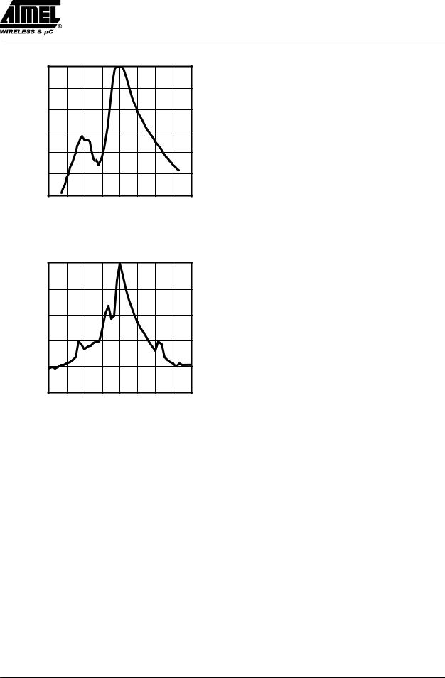
The RF receiver T5760/T5761 can be operated with and without a SAW front-end filter. In a typical automotive application, a SAW filter is used to achieve better selectivity and large signal capability. The receiving frequency response without a SAW front-end filter is illustrated in figures 6 and 7. This example relates to ASK mode. FSK mode exhibit similar behavior. The plots are printed relatively to the maximum sensitivity. If a SAW filter is used, an insertion loss of about 3 dB must be considered, but the over all selectivity is much better.
When designing the system in terms of receiving bandwidth, the LO deviation must be considered as it also determines the IF center frequency. The total LO deviation is calculated to be the sum of the deviation of the crystal and the XTO deviation of the T5760/T5761. Lowcost crystals are specified to be within ± 90 ppm over tolerance, temperature and aging. The XTO deviation of the T5760/T5761 is an additional deviation due to the XTO circuit. This deviation is specified to be ± 30 ppm worst case for a crystal with CM = 7 fF. If a crystal of
± 90 ppm is used, the total deviation is ± 120 ppm in that case. Note that the receiving bandwidth and the IF-filter bandwidth are equivalent in ASK mode but not in FSK mode.
Rev. A2, 19-Oct-00 |
5 (32) |
Preliminary Information
T5760 / T5761 |
|
|
|
|
|
|
|
|
|||||
0 |
|
|
|
|
|
|
|
|
single bi-directional line to save ports to the connected mC |
||||
|
|
|
|
|
|
|
|
or it can be operated by up to five uni-directional ports. |
|||||
|
|
|
|
|
|
|
|
|
|||||
–10 |
|
|
|
|
|
|
|
|
Basic Clock Cycle of the Digital Circuitry |
|
|||
–20 |
|
|
|
|
|
|
|
|
The complete timing of |
the digital circuitry and |
the |
||
|
|
|
|
|
|
|
|
analog filtering is derived from one clock. This clock |
|||||
) |
|
|
|
|
|
|
|
|
|||||
( dB |
|
|
|
|
|
|
|
|
cycle TClk is derived from the crystal oscillator (XTO) in |
||||
–30 |
|
|
|
|
|
|
|
|
combination with a divide by 14 circuit. According to |
||||
dP |
|
|
|
|
|
|
|
|
|||||
–40 |
|
|
|
|
|
|
|
|
chapter ‘RF Front End’, the frequency of the crystal oscil- |
||||
|
|
|
|
|
|
|
|
lator (fXTO) is defined by the RF input signal (fRFin) which |
|||||
|
|
|
|
|
|
|
|
|
|||||
–50 |
|
|
|
|
|
|
|
|
also defines the operating frequency of the local oscillator |
||||
|
|
|
|
|
|
|
|
(fLO). The basic clock cycle is TClk = 14/ fXTO giving |
|||||
|
|
|
|
|
|
|
|
|
|||||
–60 |
|
|
|
|
|
|
|
|
TClk = 2.066 ms |
for |
fRF = 868.3 MHz |
and |
|
–4 |
–3 |
–2 |
–1 |
0 |
1 |
2 |
3 |
4 |
TClk = 1.961 ms for fRF = 915 MHz |
|
|||
|
|
|
|
df ( MHz ) |
|
|
|
TClk controls the following application-relevant parame- |
|||||
Figure 6. Narrow band receiving frequency response |
ters: |
|
|
|
|||||||||
|
Timing of the polling circuit including bit check |
|
|||||||||||
|
|
|
|
|
|
|
|
|
D |
|
|||
|
0 |
|
|
|
|
|
|
|
|
|
–20 |
|
|
|
|
|
|
|
|
) |
–40 |
|
|
|
|
|
|
|
|
( dB |
|
|
|
|
|
|
|
|
|
|
|
|
|
|
|
|
|
|
|
dP |
–60 |
|
|
|
|
|
|
|
|
|
|
|
|
|
|
|
|
|
|
|
–80 |
|
|
|
|
|
|
|
|
|
–100 |
|
|
|
|
|
|
|
|
|
–12 |
–9 |
–6 |
–3 |
0 |
3 |
6 |
9 |
12 |
df ( MHz )
Figure 7. Wide band receiving frequency response
Polling Circuit and Control Logic
The receiver is designed to consume less than 1 mA while being sensitive to signals from a corresponding transmitter. This is achieved via the polling circuit. This circuit enables the signal path periodically for a short time. During this time the bit-check logic verifies the presence of a valid transmitter signal. Only if a valid signal is detected the receiver remains active and transfers the data to the connected µ C. If there is no valid signal present the receiver is in sleep mode most of the time resulting in low current consumption. This condition is called polling mode. A connected µ C is disabled during that time.
All relevant parameters of the polling logic can be configured by the connected µ C. This flexibility enables the user to meet the specifications in terms of current consumption, system response time, data rate etc.
Regarding the number of connection wires to the mC, the receiver is very flexible. It can be either operated by a
DTiming of the analog and digital signal processing
DTiming of the register programming
DFrequency of the reset marker
DIF filter center frequency (fIF0)
Most applications are dominated by two transmission fre-
quencies: fTransmit = 915 MHz is mainly used in USA, fTransmit = 868.3 MHz in Europe. In order to ease the usage of all TClk-dependent parameters on this electrical characteristics display three conditions for each parameter.
DApplication USA
(fXTO = 7.14063 MHz, TClk = 1.961 µ s)
DApplication Europe
(fXTO = 6.77617 MHz, TClk = 2.066 µ s)
DOther applications
The electrical characteristic is given as a function of TClk.
The clock cycle of some function blocks depends on the selected baud-rate range (BR_Range) which is defined in the OPMODE register. This clock cycle TXClk is defined by the following formulas for further reference:
BR_Range = BR_Range0: TXClk = 8 × TClk BR_Range1: TXClk = 4 × TClk BR_Range2: TXClk = 2 × TClk BR_Range3: TXClk = 1 × TClk
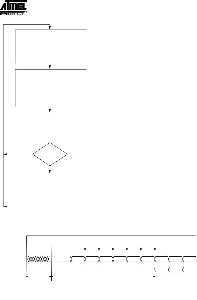
Polling Mode
According to figure 11, the receiver stays in polling mode in a continuous cycle of three different modes. In sleep mode the signal processing circuitry is disabled for the
time period TSleep while consuming low current of IS = ISoff. During the start-up period, TStartup, all signal processing circuits are enabled and settled. In the follow-
6 (32) |
Rev. A2, 19-Oct-00 |
Preliminary Information

T5760 / T5761
ing bit-check mode, the incoming data stream is analyzed bit by bit contra a valid transmitter signal. If no valid signal is present, the receiver is set back to sleep mode af-
ter the period TBit-check. This period varies check by check as it is a statistical process. An average value for
TBit-check is given in the electrical characteristics. During
TStartup and TBit-check the current consumption is IS = ISon. The condition of the receiver is indicated on Pin IC_AC-
TIVE. The average current consumption in polling mode is dependent on the duty cycle of the active mode and can be calculated as:
ISpoll + |
ISoff TSleep ) ISon |
(TStartup ) TBitcheck) |
|
TSleep ) TStartup |
) TBitcheck |
||
|
During TSleep and TStartup the receiver is not sensitive to a transmitter signal. To guarantee the reception of a trans-
mitted command the transmitter must start the telegram with an adequate preburst. The required length of the preburst depends on the polling parameters TSleep,
TStartup, TBit-check and the start-up time of a connected C (TStart, C). Thus, TBit-check depends on the actual bit rate and the number of bits (NBit-check) to be tested.
The following formula indicates how to calculate the preburst length.
TPreburst w TSleep + TStartup + TBit-check + TStart_mC
Sleep Mode
The length of period TSleep is defined by the 5-bit word Sleep of the OPMODE register, the extension factor
XSleep (according to table 9), and the basic clock cycle TClk. It is calculated to be:
TSleep = Sleep XSleep 1024 TClk
In USand European applications, the maximum value of
TSleep is about 60 ms if XSleep is set to 1. The time resolution is about 2 ms in that case. The sleep time can be
extended to almost half a second by setting XSleep to 8. XSleep can be set to 8 by bit XSleepStd to’1’.
According to table 8, the highest register value of sleep sets the receiver into a permanent sleep condition. The receiver remains in that condition until another value for Sleep is programmed into the OPMODE register. This function is desirable where several devices share a single data line and may also be used for C polling – via Pin POLLING/_ON, the receiver can be switched on and off.
Rev. A2, 19-Oct-00 |
7 (32) |
Preliminary Information
T5760 / T5761
Sleep mode:
All circuits for signal processing are disabled. Only XTO and Polling logic is enabled.
Output level on Pin IC_ACTIVE => low
IS = ISoff
TSleep = Sleep × XSleep × 1024 × TClk
Start-up mode:
The signal processing circuits are enabled.
After the start-up time (TStartup) all circuits are in stable condition and ready to receive.
Output level on Pin IC_ACTIVE => high IS = ISon
TStartup
Sleep: |
5-bit word defined by Sleep0 to |
|
Sleep4 in OPMODE register |
XSleep: |
Extension factor defined by |
|
XSleepStd |
|
according to table 9 |
TClk: |
Basic clock cycle defined by fXTO |
|
and Pin MODE |
TStartup: |
Is defined by the selected baud rate |
|
range and TClk. The baud-rate range |
|
is defined by Baud0 and Baud1 in |
|
the OPMODE register. |
|
|
|
Bit-check mode: |
|
|
|
|
|
|
|
|
||||||||||
|
|
|
The incomming data stream is analyzed. If |
TBit-check: |
Depends on the result of the |
||||||||||||||||
|
|
|
the timing indicates a valid transmitter |
|
|
|
bit check |
|
|
|
|||||||||||
|
|
|
signal, the receiver is set to receiving mode. |
|
|
|
|
|
|
|
|
||||||||||
|
|
|
Otherwise it is set to Sleep mode. |
|
|
|
If the bit check is ok, TBit-check |
||||||||||||||
|
|
|
Output level on Pin IC_ACTIVE => high |
|
|
|
depends on the number of bits to be |
||||||||||||||
|
|
|
IS = ISon |
|
|
|
checked (N |
|
) and on the |
||||||||||||
|
|
|
TBit-check |
|
|
|
|
Bit-check |
|
|
|||||||||||
|
|
|
|
|
|
utilized data rate. |
|
|
|||||||||||||
|
|
|
|
|
|
|
Bit check |
|
|
|
If the bit check fails, the average |
||||||||||
|
|
NO |
|
|
|
|
OK ? |
|
|
|
|||||||||||
|
|
|
|
|
|
|
|
|
time period for that check depends |
||||||||||||
|
|
|
|
|
|
|
|
|
|
|
|
|
|
|
|
|
|||||
|
|
|
|
|
|
|
|
|
|
|
|
|
|
|
|
|
on the selected baud-rate range and |
||||
|
|
|
|
|
|
|
|
|
|
|
|
|
|
|
|
|
on TClk. The baud-rate range is |
||||
|
|
|
|
|
|
|
|
YES |
|
|
|
||||||||||
|
|
|
|
|
|
|
|
|
|
|
defined by Baud0 and Baud1 in the |
||||||||||
|
|
|
Receiving mode: |
|
|
|
|||||||||||||||
|
|
|
|
|
|
OPMODE register. |
|
|
|||||||||||||
|
|
|
The receiver is turned on permanently and |
|
|
|
|
|
|||||||||||||
|
|
|
|
|
|
|
|
|
|
|
|||||||||||
|
|
|
passes the data stream to the connected mC. |
|
|
|
|
|
|
|
|
||||||||||
|
|
|
It can be set to Sleep mode through an OFF |
|
|
|
|
|
|
|
|
||||||||||
|
|
|
command via Pin DATA or POLLING/_ON. |
|
|
|
|
|
|
|
|
||||||||||
|
|
|
Output level on Pin IC_ACTIVE => high |
|
|
|
|
|
|
|
|
||||||||||
|
|
|
IS = ISon |
|
|
|
|
|
|
|
|
||||||||||
|
|
|
|
|
|
|
OFF command |
|
|
|
|
|
|
|
|
|
|
|
|||
|
|
|
|
|
|
|
|
|
|
|
|
|
|
|
|||||||
|
|
|
|
|
|
|
|
|
|
|
|
|
|
|
|
|
|
|
|
|
|
|
|
|
|
|
|
|
|
|
|
|
|
|
|
|
|
|
|
|
|
|
|
|
|
|
|
|
|
|
|
|
|
|
Figure 8. Polling mode flow chart |
|
|
|
|||||||
( Number of checked Bits: 3 ) |
|
|
Bit check ok |
|
|
|
|||||||||||||||
IC_ACTIVE |
|
|
|
|
|
|
|
|
|
||||||||||||
Bit check |
|
|
|
|
|
|
|
|
|
|
|
|
|
|
|
|
|
|
|
||
|
|
|
|
|
|
|
|
1/2 Bit |
1/2 Bit 1/2 Bit |
1/2 Bit 1/2 Bit |
1/2 Bit |
||||||||||
|
|
|
|
|
|
|
|
|
|
|
|||||||||||
Dem_out |
|
|
|
|
|
|
|
|
|
|
|
|
|
|
|
|
|
|
|
||
|
|
|
|
|
|
|
|
|
|
|
|
|
|
|
|
|
|
|
|||
|
|
|
|
|
|
|
|
|
|
|
|
|
|||||||||
Data_out (DATA) |
TBit–check |
|
|
|
|
|
|||||||||||||||
|
|
|
|
|
|
TStart–up |
|
|
|
|
|
||||||||||
|
|
|
|
|
Start–up mode |
Bit–check mode |
|
|
|
|
Receiving mode |
||||||||||
Figure 9. Timing diagram for complete successful bit check
8 (32) Rev. A2, 19-Oct-00
Preliminary Information
T5760 / T5761
Bit-Check Mode
In bit-check mode the incoming data stream is examined to distinguish between a valid signal from a corresponding transmitter and signals due to noise. This is done by subsequent time frame checks where the distances between 2 signal edges are continuously compared to a programmable time window. The maximum count of this edge-to-edge tests before the receiver switches to receiving mode is also programmable.
Configuring the Bit Check
Assuming a modulation scheme that contains 2 edges per bit, two time frame checks are verifying one bit. This is valid for Manchester, Bi-phase and most other modulation schemes. The maximum count of bits to be checked
can be set to 0, 3, 6 or 9 bits via the variable NBit-check in the OPMODE register. This implies 0, 6, 12 and 18 edge
to edge checks respectively. If NBit-check is set to a higher value, the receiver is less likely to switch to receiving mode due to noise. In the presence of a valid transmitter
signal, the bit check takes less time if NBit-check is set to a lower value. In polling mode, the bit-check time is not
dependent on NBit-check. Figure 12 shows an example where 3 bits are tested successfully and the data signal is
transferred to Pin DATA.
According to figure 13, the time window for the bit check is defined by two separate time limits. If the edge-to-edge
time tee is in between the lower bit-check limit TLim_min and the upper bit-check limit TLim_max, the check will be continued. If tee is smaller than TLim_min or tee exceeds
T , the bit check will be terminated and the receiver switches to sleep mode.
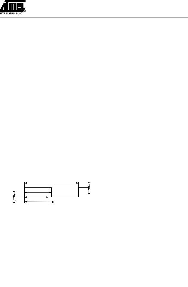
1/fSig
tee
Dem_out
TLim_min
TLim_max
Figure 10. Valid time window for bit check
For best noise immunity it is recommended to use a low span between TLim_min and TLim_max. This is achieved us-
ing a fixed frequency at a 50% duty cycle for the transmitter preburst. A ‘11111...’ or a ‘10101...’ sequence in Manchester or Bi-phase is a good choice concerning that advice. A good compromise between receiver sensitivity and susceptibility to noise is a time window of
± 25% regarding the expected edge-to-edge time tee. Using pre-burst patterns that contain various edge-to-edge time periods, the bit-check limits must be programmed according to the required span.
The bit-check limits are determined by means of the formula below.
TLim_min = Lim_min × TXClk
TLim_max = (Lim_max –1) × TXClk
Lim_min and Lim_max are defined by a 5-bit word each within the LIMIT register.
Using above formulas, Lim_min and Lim_max can be determined according to the required TLim_min, TLim_max and TXClk. The time resolution defining TLim_min and TLim_max is TXClk. The minimum edge-to-edge time tee (tDATA_L_min, tDATA_H_min) is defined according to the chapter ‘Receiving Mode’. The lower limit should be set to Lim_min ≥ 10. The maximum value of the upper limit is Lim_max = 63.
If the calculated value for Lim_min is < 19, it is recom-
mended to check 6 or 9 bits (NBit-check) to prevent switching to receiving mode due to noise.
Figures 14, 15 and 16 illustrate the bit check for the bitcheck limits Lim_min = 14 and Lim_max = 24. When the IC is enabled, the signal processing circuits are en-
abled during TStartup. The output of the ASK/ FSK demodulator (Dem_out) is undefined during that period.
When the bit check becomes active, the bit-check counter is clocked with the cycle TXClk.
Figure 14 shows how the bit check proceeds if the bitcheck counter value CV_Lim is within the limits defined by Lim_min and Lim_max at the occurrence of a signal edge. In figure 15 the bit check fails as the value CV_lim is lower than the limit Lim_min. The bit check also fails if CV_Lim reaches Lim_max. This is illustrated in figure 16.
Rev. A2, 19-Oct-00 |
9 (32) |
Preliminary Information

T5760 / T5761
( Lim_min = 14, Lim_max = 24 ) |
Bit check ok |
Bit check ok |
IC_ACTIVE |
|
|
|
|
|
|
|
|
|
|
|
|
|
|
|
|
|
|
|
|
|
|
|
|
|
|
|
|
|
|
|
|
Bit check |
|
|
|
|
|
|
|
|
|
|
|
|
|
|
|
|
|
|
|
|
|
|
|
|
|
|
|
|
|
|
|
|
|
|
|
|
|
|
|
|
|
|
|
|
|
|
|
|
|
1/2 Bit |
|
|
|
|
|
|
1/2 Bit |
|
1/2 Bit |
||||||
Dem_out |
|
|
|
|
|
|
|
|
|
|
|
|
|
|
|
|
|
|
|
|
|
|
|
|
|
|
|
|
|
|
|
|
Bit–check– |
0 |
1 |
2 |
3 |
4 |
5 |
6 |
7 |
8 |
1 |
2 |
3 |
4 |
5 |
6 |
7 |
8 |
9 10 11 12 13 14 15 16 17 18 |
1 |
2 |
3 |
4 |
5 |
6 |
7 |
8 |
9 10 11 12 13 14 15 |
1 |
2 |
3 |
4 |
|
counter |
||||||||||||||||||||||||||||||||
|
|
|
|
|
|
|
|
|
|
|
|
|
|
|
|
|
|
|
|
|
|
|
|
|
|
|
|
|
|
|
||
|
TStart–up |
|
|
|
|
|
|
TXClk |
|
|
|
|
|
|
|
|
TBit–check |
|
|
|
|
|
|
|
|
|
|
|
|
|
||
|
Start–up mode |
|
|
|
|
|
|
|
|
|
|
|
|
|
|
|
|
Bit–check mode |
|
|
|
|
|
|
|
|
|
|
|
|
|
|
|
|
|
|
|
|
|
Figure 11. Timing diagram during bit check |
|
|
|
|
|
|
|
|
|
|
|
|
|
||||||||||||
( Lim_min = 14, Lim_max = 24 ) |
|
|
|
|
|
|
|
|
|
|
|
|
|
|
Bit check failed ( CV_Lim < Lim_min ) |
|
|
|
|
|
|
|
|
|||||||||
|
|
|
|
|
|
|
|
|
|
|
|
|
|
|
|
|
|
|
|
|
|
|
|
|||||||||
IC_ACTIVE |
|
|
|
|
|
|
|
|
|
|
|
|
|
|
|
|
|
|
Bit check |
|
|
|
|
|
|
|
|
|
|
|
|
|
|
|
|
|
|
|
|
|
|
|
|
|
|
|
|
|
|
|
1/2 Bit |
|
|
|||
Dem_out |
|
|
|
|
|
|
|
|
|
|
|
|
|
|
|
|
|
|
Bit–check– |
0 |
1 |
2 |
3 |
4 |
5 |
6 |
1 |
2 |
3 |
4 |
5 |
6 |
7 |
8 |
9 10 11 12 |
0 |
|
counter |
||||||||||||||||||
|
|
|
|
|
|
|
|
|
|
|
|
|
|
|
|
|
||
|
TStart–up |
|
|
|
|
|
|
|
|
TBit–check |
|
|
|
TSleep |
||||
|
Start–up mode |
|
|
|
|
|
|
|
Bit–check mode |
|
Sleep mode |
|||||||
Figure 12. Timing diagram for failed bit check (condition: CV_Lim < Lim_min)
( Lim_min = 14, Lim_max = 24 ) |
|
|
|
|
|
|
|
|
|
|
|
|
|
|
|
|
|
|
|
|
|
|
|
|
|
|
|
|
|
Bit check failed ( CV_Lim >= Lim_max ) |
||||||||||
IC_ACTIVE |
|
|
|
|
|
|
|
|
|
|
|
|
|
|
|
|
|
|
|
|
|
|
|
|
|
|
|
|
|
|
|
|
|
|
|
|
|
|
|
|
|
|
|
|
|
|
|
|
|
|
|
|
|
|
|
|
|
|
|
|
|
|
|
|
|
|
|
|
|
|
|
|
|
|
|
|
|
|
|
|
|
Bit check |
|
|
|
|
|
|
|
|
|
|
|
|
|
|
|
|
|
|
|
|
|
|
|
|
|
|
|
|
|
|
|
|
|
|
|
|
|
|
|
|
|
|
|
|
|
|
|
|
|
|
|
|
|
|
|
|
|
|
|
|
|
|
|
|
|
|
|
|
|
|
|
|
|
|
|
|
|
|
|
|
|
Dem_out |
|
|
|
|
|
|
|
|
|
|
|
|
|
|
|
|
|
|
|
|
|
|
|
|
1/2 Bit |
|
|
|
|
|
|
|
|
|
|
|||||
|
|
|
|
|
|
|
|
|
|
|
|
|
|
|
|
|
|
|
|
|
|
|
|
|
|
|
|
|
|
|
|
|
|
|
|
|
|
|
|
|
|
|
|
|
|
|
|
|
|
|
|
|
|
|
|
|
|
|
|
|
|
|
|
|
|
|
|
|
|
|
|
|
|
|
|
|
|
|
|
|
|
Bit–check– |
|
|
|
|
|
|
|
|
|
|
|
|
|
|
|
|
|
|
|
|
|
|
|
|
|
|
|
|
|
|
|
|
|
|
|
|
|
|
|
|
0 |
|
|
1 |
2 |
3 |
4 |
5 |
6 |
7 |
1 |
2 |
3 |
4 |
|
5 |
6 |
7 |
8 |
9 |
10 |
11 |
12 |
13 |
14 |
15 |
16 |
17 |
18 |
19 |
20 |
21 |
22 |
23 |
24 |
0 |
|||||
counter |
|
|
|
|||||||||||||||||||||||||||||||||||||
|
|
TStart–up |
|
|
|
|
|
|
|
|
|
|
|
|
|
|
|
TBit–check |
|
|
|
|
|
|
|
|
|
|
|
|
|
|
|
|
TSleep |
|||||
|
|
|
|
|
|
|
|
|
|
|
|
|
|
|
|
|
|
|
|
|
|
|
|
|
|
|
|
|
|
|
|
|
|
|||||||
|
|
|
Start–up mode |
|
|
|
|
|
|
|
|
|
|
|
|
|
Bit–check mode |
|
|
|
|
|
|
|
|
|
Sleep mode |
|||||||||||||
Figure 13. Timing diagram for failed bit check (condition: CV_Lim > = Lim_max)
Duration of the Bit Check
If no transmitter signal is present during the bit check, the output of the ASK/ FSK demodulator delivers random
signals. The bit check is a statistical process and TBit-check varies for each check. Therefore, an average value for
TBit-check is given in the electrical characteristics. TBit-check depends on the selected baud-rate range and on TClk. A higher baud-rate range causes a lower value for
TBit-check resulting in a lower current consumption in polling mode.
In the presence of a valid transmitter signal, TBit-check is dependent on the frequency of that signal, fSig, and the
count of the checked bits, NBit-check. A higher value for
NBit-check thereby results in a longer period for TBit-check requiring a higher value for the transmitter pre-burst
TPreburst.
Receiving Mode
If the bit check was successful for all bits specified by NBit-check, the receiver switches to receiving mode. According to figure 9, the internal data signal is switched to Pin DATA in that case and the data clock is available after the start bit has been detected (figure 20). A connected C can be woken up by the negative edge at Pin DATA or by the data clock at Pin DATA_CLK. The receiver stays in that condition until it is switched back to polling mode explicitly.
10 (32) |
Rev. A2, 19-Oct-00 |
Preliminary Information
 Loading...