


Features
•Two Different IF Receiving Bandwidth Versions Are Available (BIF = 300 kHz or 600 kHz)
•5 V to 20 V Automotive Compatible Data Interface
•IC Condition Indicator, Sleep or Active Mode
•Low Power Consumption Due to Configurable Self Polling with a Programmable Timeframe Check
•High Sensitivity, Especially at Low Data Rates
•Data Clock Available for Manchesterand Bi-phase-coded Signals
•Minimal External Circuitry Requirements, no RF Components on the PC Board Except Matching to the Receiver Antenna
•Sensitivity Reduction Possible Even While Receiving
•Fully Integrated VCO
•SO20 Package
•Supply Voltage 4.5 V to 5.5 V, Operating Temperature Range -40°C to +105°C
•Single-ended RF Input for Easy Adaptation to λ/4 Antenna or Printed Antenna on PCB
•Low-cost Solution Due to High Integration Level
•ESD Protection According to MIL-STD. 883 (4KV HBM)
•High Image Frequency Suppression Due to 1 MHz IF in Conjunction with a SAW Frontend Filter. Up to 40 dB is Thereby Achievable With State-of-the-art SAWs.
•Communication to Microcontroller Possible Via a Single, Bi-directional Data Line
•Power Management (Polling) Is Also Possible by Means of a Separate Pin Via the Microcontroller
•Programmable Digital Noise Suppression
Description
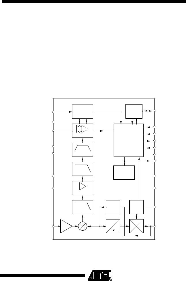
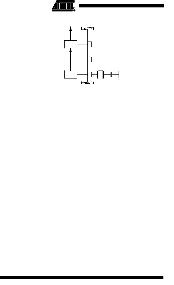
The T5743 is a multi-chip PLL receiver device supplied in an SO20 package. It has been especially developed for the demands of RF low-cost data transmission systems with data rates from 1 kBaud to 10 kBaud in Manchester or Bi-phase code. The receiver is well suited to operate with Atmel's PLL RF transmitter U2741B. Its main applications are in the areas of telemetering, security technology and keyless-entry systems. It can be used in the frequency receiving range of f0 = 300 MHz to 450 MHz for ASK or FSK data transmission. All the statements made below refer to 433.92 MHz and 315 MHz applications.
System Block Diagram |
|
|
|
|
|
|
Figure 1. System Block Diagram |
|
|
|
|
|
|
UHF ASK/FSK |
|
UHF ASK/FSK |
|
|
|
|
Remote control transmitter |
|
Remote control receiver |
|
|
|
|
U2741B |
|
T5743 |
Demod. |
|
1...5 |
|
|
|
|
Control |
µC |
||
|
|
|
|
|
||
XTO |
PLL |
|
|
|
|
|
|
|
|
IF Amp |
|
|
|
|
Antenna |
Antenna |
|
|
|
|
|
VCO |
|
PLL |
XTO |
|
|
|
|
|
|
|
||
|
Power |
LNA |
VCO |
|
|
|
|
amp. |
|
|
|
||
|
|
|
|
|
|
|
UHF ASK/FSK
Receiver
T5743
Preliminary
Rev. 4569A–RKE–12/02
1
Pin Configuration
Figure 2. Pinning SO20
SENS |
1 |
20 |
DATA |
IC_ACTIVE |
2 |
19 |
POLLING/_ON |
CDEM |
3 |
18 |
DGND |
AVCC |
4 |
17 |
DATA_CLK |
|
|
|
|
TEST |
5 |
16 |
MODE |
|
|
T5743 |
|
AGND |
6 |
15 |
DVCC |
MIXVCC |
7 |
14 |
XTO |
|
|
||
LNAGND |
8 |
13 |
LFGND |
LNA_IN |
9 |
12 |
LF |
n.c. |
10 |
11 |
LFVCC |
Pin Description
Pin |
Symbol |
Function |
|
|
|
1 |
SENS |
Sensitivity-control resistor |
|
|
|
2 |
IC_ACTIVE |
IC condition indicator |
|
|
Low = sleep mode |
|
|
High = active mode |
|
|
|
3 |
CDEM |
Lower cut-off frequency data filter |
|
|
|
4 |
AVCC |
Analog power supply |
|
|
|
5 |
TEST |
Test pin, during operation at GND |
|
|
|
6 |
AGND |
Analog ground |
|
|
|
7 |
MIXVCC |
Power supply mixer |
|
|
|
8 |
LNAGND |
High-frequency ground LNA and mixer |
|
|
|
9 |
LNA_IN |
RF input |
|
|
|
10 |
n.c. |
Not connected |
|
|
|
11 |
LFVCC |
Power supply VCO |
|
|
|
12 |
LF |
Loop filter |
|
|
|
13 |
LFGND |
Ground VCO |
|
|
|
14 |
XTO |
Crystal oscillator |
|
|
|
2 T5743
4569A–RKE–12/02
T5743
Pin Description (Continued)
Pin |
Symbol |
Function |
|
|
|
15 |
DVCC |
Digital power supply |
|
|
|
16 |
MODE |
Selecting 433.92 MHz/315 MHz |
|
|
Low: fXT0 = 4.90625 MHz (USA) |
|
|
High: fXT0 = 6.76438 MHz (Europe) |
17 |
DATA_CLK |
Bit clock of data stream |
|
|
|
18 |
DGND |
Digital ground |
|
|
|
19 |
POLLING/_ON |
Selects polling or receiving mode |
|
|
Low: receiving mode |
|
|
High: polling mode |
|
|
|
20 |
DATA |
Data output/configuration input |
|
|
|
Figure 3. Block Diagram
|
FSK/ASK- |
Dem_out |
|
Data |
DATA |
|
CDEM |
Demodulator |
|
|
interface |
||
|
and data filter |
|
|
|
|
|
AVCC |
RSSI |
Limiter out |
|
|
|
|
SENS |
|
|
|
|
|
POLLING/_ON |
|
|
Sensitivity |
|
|
TEST |
|
|
|
IF Amp |
Polling circuit |
|||
|
|
reduction |
|
|||
|
|
|
|
and |
DATA_CLK |
|
|
|
|
|
|
||
|
|
|
|
control logic |
||
|
|
|
|
|
||
AGND |
|
|
|
|
|
MODE |
|
|
|
|
|
|
|
DGND |
|
4. Order |
|
FE |
CLK |
DVCC |
|
|
|
|
|||
|
|
|
|
|
|
IC_ACTIVE |
|
|
LPF |
|
Standby logic |
|
|
MIXVCC |
|
3 MHz |
|
LFGND |
||
|
|
|
|
|
||
LNAGND |
|
|
|
|
|
LFVCC |
|
|
IF Amp |
|
|
|
|
|
|
LPF |
|
VCO |
XTO |
XTO |
|
|
3 MHz |
|
|
|
|
LNA_IN |
LNA |
|
|
f |
|
LF |
|
|
64 |
|
|||
|
|
|
|
|
|
|
3
4569A–RKE–12/02
RF Front-end
The RF front-end of the receiver is a heterodyne configuration that converts the input signal into a 1 MHz IF signal. According to Figure 3, the front-end consists of an LNA (low-noise amplifier), LO (local oscillator), a mixer and an RF amplifier.
The LO generates the carrier frequency for the mixer via a PLL synthesizer. The XTO (crystal oscillator) generates the reference frequency fXTO. The VCO (voltage-controlled oscillator) generates the drive voltage frequency fLO for the mixer. fLO is dependent on the voltage at Pin LF. fLO is divided by factor 64. The divided frequency is compared to fXTO by the phase frequency detector. The current output of the phase frequency detector is connected to a passive loop filter and thereby generates the control voltage VLF for the VCO. By means of that configuration VLF is controlled in a way that fLO/64 is equal to fXTO. If fLO is determined, fXTO can be calculated using the following formula: fXTO = fLO/64.
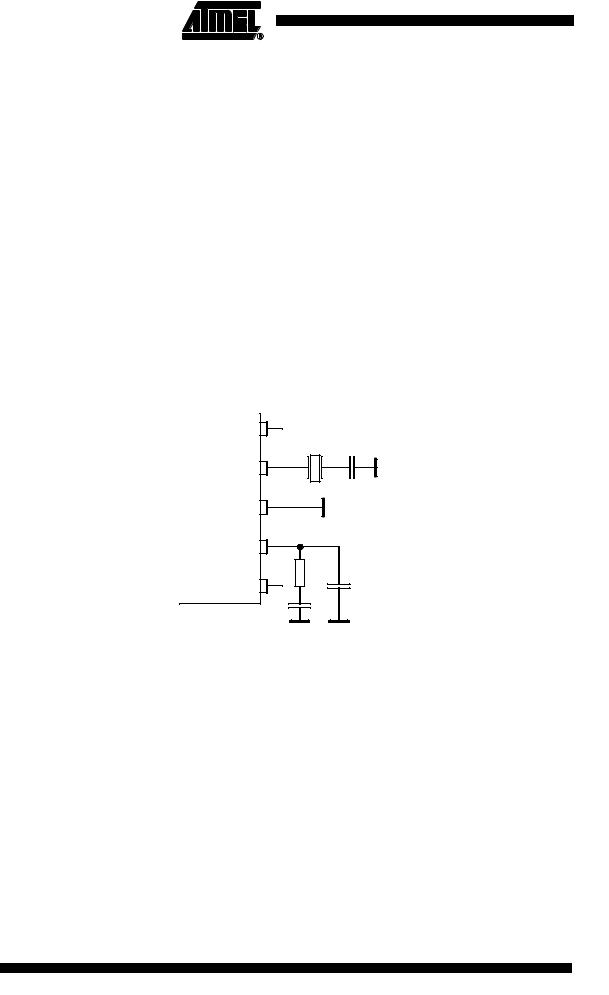
The XTO is a one-pin oscillator that operates at the series resonance of the quartz crystal. According to Figure 4, the crystal should be connected to GND via a capacitor CL. The value of that capacitor is recommended by the crystal supplier. The value of CL should be optimized for the individual board layout to achieve the exact value of fXTO and hereby of fLO. When designing the system in terms of receiving bandwidth, the accuracy of the crystal and the XTO must be considered.
Figure 4. PLL Peripherals
VS
DVCC
CL
XTO
LFGND |
|
R1 = 820 |
|
|
C9 = 4.7 nF |
LF |
|
C10 = 1 nF |
|
|
|
VS |
R1 |
C10 |
LFVCC |
|
|
|
C9 |
|
The passive loop filter connected to Pin LF is designed for a loop bandwidth of BLoop = 100 kHz. This value for BLoop exhibits the best possible noise performance of the LO. Figure 4 shows the appropriate loop filter components to achieve the desired loop bandwidth. If the filter components are changed for any reason please notify that the maximum capacitive load at Pin LF is limited. If the capacitive load is exceeded, a bit check may no longer be possible since fLO cannot settle in time before the bit check starts to evaluate the incoming data stream. Self polling does therefore also not work in that case.
fLO is determined by the RF input frequency fRF and the IF frequency fIF using the following formula: fLO = fRF - fIF
To determine fLO, the construction of the IF filter must be considered at this point. The nominal IF frequency is fIF = 1 MHz. To achieve a good accuracy of the filter’s corner frequencies, the filter is tuned by the crystal frequency fXTO. This means that there is a fixed relation between fIF and fLO. This relation is dependent on the logic level at Pin MODE.
4 T5743
4569A–RKE–12/02
T5743
This is described by the following formulas:
MODE 0 (USA) : f fLO
= IF = ---------
314
MODE 1 (Europe) : f fLO
= IF = -----------------
432.92
The relation is designed to achieve the nominal IF frequency of fIF = 1 MHz for most applications. For applications where fRF = 315 MHz, MODE must be set to ‘0’. In the case of fRF = 433.92 MHz, MODE must be set to ‘1’. For other RF frequencies, fIF is not equal to 1 MHz. fIF is then dependent on the logical level at Pin MODE and on fRF. Table 1 summarizes the different conditions.
The RF input either from an antenna or from a generator must be transformed to the RF input Pin LNA_IN. The input impedance of that pin is provided in the electrical parameters. The parasitic board inductances and capacitances also influence the input matching. The RF receiver T5743 exhibits its highest sensitivity at the best signal-to- noise ratio in the LNA. Hence, noise matching is the best choice for designing the transformation network.
A good practice when designing the network is to start with power matching. From that starting point, the values of the components can be varied to some extent to achieve the best sensitivity.
If a SAW is implemented into the input network a mirror frequency suppression ofPRef = 40 dB can be achieved. There are SAWs available that exhibit a notch atf = 2 MHz. These SAWs work best for an intermediate frequency of fIF = 1 MHz. The selectivity of the receiver is also improved by using a SAW. In typical automotive applications, a SAW is used.
Figure 5 shows a typical input matching network, for fRF = 315 MHz and fRF = 433.92 MHz using a SAW. Figure 6 illustrates an according input matching to 50 without a SAW. The input matching networks shown in Figure 6 are the reference networks for the parameters given in the electrical characteristics.
Table 1. Calculation of LO and IF Frequency
Conditions |
Local Oscillator Frequency Intermediate Frequency |
fRF = 315 MHz, MODE = 0 |
fLO = 314 MHz |
fIF = 1 MHz |
||||
fRF = 433.92 MHz, MODE = 1 |
fLO = 432.92 MHz |
fIF = 1 MHz |
||||
300 MHz < fRF < 365 MHz, |
|
|
fRF |
|
fLO |
|
MODE = 0 |
fLO |
= ----- |
+----- |
----1----- |
fIF = |
314--------- |
|
|
1 |
|
|||
|
|
|
|
314 |
|
|
|
|
|
|
|
|
|
365 MHz < fRF < 450 MHz, |
|
|
|
fRF |
|
fLO |
MODE = 1 |
fLO |
= ----- |
+----- |
--------1--------- |
fIF = 432.92----------------- |
|
|
|
1 |
432.92----------------- |
|
|
|
5
4569A–RKE–12/02
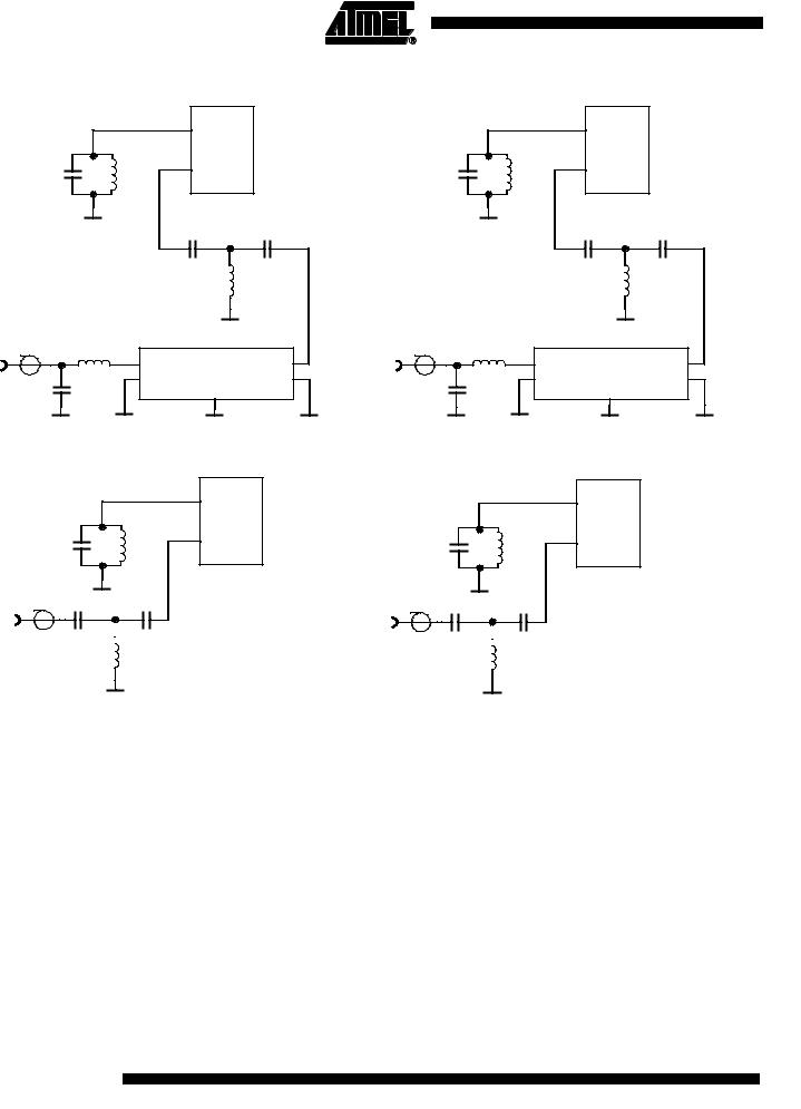
Figure 5. Input Matching Network with SAW Filter
8 LNAGND
|
|
|
|
9 |
T5743 |
|
||
|
C3 |
L |
|
LNA_IN |
|
|
||
|
|
|
|
|
|
|
||
|
22p |
25n |
|
|
|
|
|
|
|
|
|
|
C16 |
|
C17 |
|
|
fRF = 433.92 MHz |
|
|
100p |
L3 |
8.2p |
|
||
|
|
|
27n |
F27NJ |
|
|||
|
|
|
|
|
|
|
TOKO LL2012 |
|
|
L2 |
|
|
|
|
|
|
|
RFIN |
TOKO LL2012 |
|
|
|
|
|
|
|
F33NJ |
1 |
|
|
B3555 |
|
5 |
||
|
33n |
IN |
|
OUT |
||||
|
2 |
|
|
|
6 |
|||
|
IN_GND |
|
|
OUT_GND |
||||
|
C2 |
|
|
|
|
|||
|
8.2p |
|
|
|
CASE_GND |
|
||
|
|
|
|
3,4 |
7,8 |
|
|
|
|
|
|
|
|
|
|
||
Figure 6. Input Matching Network without SAW Filter
fRF = 433.92 MHz |
8 |
LNAGND |
|
||
|
9 |
T5743 |
15p |
LNA_IN |
|
25n |
|
RFIN
3.3p 
 100p
100p
22n TOKO LL2012
F22NJ
8 LNAGND
|
|
|
|
9 |
T5743 |
|
||
|
C3 |
L |
|
LNA_IN |
|
|
||
|
|
|
|
|
|
|
||
|
47p |
25n |
|
|
|
|
|
|
|
|
|
|
C16 |
|
C17 |
|
|
fRF = 315 MHz |
|
|
100p |
L3 |
22p |
|
||
|
|
|
47n |
TOKO LL2012 |
||||
|
|
|
|
|
|
|
F47NJ |
|
|
L2 |
|
|
|
|
|
|
|
RFIN |
TOKO LL2012 |
|
|
|
|
|
|
|
F82NJ |
1 |
|
|
B3551 |
|
5 |
||
|
82n |
IN |
|
OUT |
||||
|
2 |
|
|
|
6 |
|||
|
IN_GND |
|
|
OUT_GND |
||||
|
C2 |
|
|
|
|
|||
|
10p |
|
|
|
CASE_GND |
|
||
|
|
|
|
3,4 |
7,8 |
|
|
|
|
|
|
|
|
|
|
||
fRF = 315 MHz |
8 |
LNAGND |
|
||
|
9 |
T5743 |
33p |
LNA_IN |
|
25n |
|
RFIN
3.3p 
 100p
100p
39n TOKO LL2012
F39NJ
Please notify that for all coupling conditions (see Figure 5 and Figure 6), the bond wire inductivity of the LNA ground is compensated. C3 forms a series resonance circuit together with the bond wire. L = 25 nH is a feed inductor to establish a DC path. Its value is not critical but must be large enough not to detune the series resonance circuit. For cost reduction this inductor can be easily printed on the PCB. This configuration improves the sensitivity of the receiver by about 1 dB to 2 dB.
6 T5743
4569A–RKE–12/02

T5743
Analog Signal Processing
IF Amplifier
RSSI Amplifier
The signals coming from the RF front-end are filtered by the fully integrated 4th-order IF filter. The IF center frequency is fIF = 1 MHz for applications where fRF = 315 MHz or fRF = 433.92 MHz is used. For other RF input frequencies refer to Table 1 to determine the center frequency.
The T5743 is available with two different IF bandwidths. T5743P3, the version with BIF = 300 kHz, is well suited for ASK systems where Atmel’s PLL transmitter U2741B is used. The receiver T5743P6 employs an IF bandwidth of BIF = 600 kHz. Both versions can be used together with the U2741B in ASK and FSK mode. If used in ASK applications, it allows higher tolerances for the receiver and PLL transmitter crystals. SAW transmitters exhibit much higher transmit freqeuncy tolerances compared to PLL transmitters. Generally, it is necessary to use BIF = 600 kHz together with such transmitters.
The subsequent RSSI amplifier enhances the output signal of the IF amplifier before it is
fed into the demodulator. The dynamic range of this amplifier is DRRSSI = 60 dB. If the RSSI amplifier is operated within its linear range, the best S/N ratio is maintained in ASK
mode. If the dynamic range is exceeded by the transmitter signal, the S/N ratio is defined by the ratio of the maximum RSSI output voltage and the RSSI output voltage due to a disturber. The dynamic range of the RSSI amplifier is exceeded if the RF input signal is about 60 dB higher compared to the RF input signal at full sensitivity.
In FSK mode the S/N ratio is not affected by the dynamic range of the RSSI amplifier.
The output voltage of the RSSI amplifier is internally compared to a threshold voltage
VTh_red. VTh_red is determined by the value of the external resistor RSens. RSens is connected between Pin SENS and GND or VS. The output of the comparator is fed into the
digital control logic. By this means it is possible to operate the receiver at a lower sensitivity.
If RSens is connected to GND, the receiver operates at full sensitivity.
If RSens is connected to VS, the receiver operates at a lower sensitivity. The reduced sensitivity is defined by the value of RSens, the maximum sensitivity by the signal-to-noise ratio of the LNA input. The reduced sensitivity depends on the signal strength at the output of the RSSI amplifier.
Since different RF input networks may exhibit slightly different values for the LNA gain, the sensitivity values given in the electrical characteristics refer to a specific input matching. This matching is illustrated in Figure 6 and exhibits the best possible sensitivity.
RSens can be connected to VS or GND via a microcontroller. The receiver can be switched from full sensitivity to reduced sensitivity or vice versa at any time. In polling
mode, the receiver will not wake up if the RF input signal does not exceed the selected sensitivity. If the receiver is already active, the data stream at Pin DATA will disappear when the input signal is lower than defined by the reduced sensitivity. Instead of the data stream, the pattern according to Figure 7 is issued at Pin DATA to indicate that the receiver is still active (see also figure 34).
Figure 7. Steady L State Limited DATA Output Pattern
DATA |
t DATA_L_max |
t DATA_min |
7
4569A–RKE–12/02

FSK/ASK Demodulator
and Data Filter
Receiving
Characteristics
The signal coming from the RSSI amplifier is converted into the raw data signal by the ASK/FSK demodulator. The operating mode of the demodulator is set via the bit ASK/_FSK in the OPMODE register. Logic ‘L’ sets the demodulator to FSK, applying ‘H’ to ASK mode.
In ASK mode, an automatic threshold control circuit (ATC) is used to set the detection reference voltage to a value where a good signal-to-noise ratio is achieved. This circuit effectively suppresses any kind of inband noise signals or competing transmitters. If the S/N (ratio to suppress inband noise signals) exceeds 10 dB, the data signal can be detected properly.
The FSK demodulator is intended to be used for an FSK deviation of 10 kHz f 100 kHz. In FSK mode the data signal can be detected if the S/N (ratio to suppress inband noise signals) exceeds 2 dB. This value is guaranteed for all modulation schemes of a disturber signal.
The output signal of the demodulator is filtered by the data filter before it is fed into the digital signal processing circuit. The data filter improves the S/N ratio as its passband can be adopted to the characteristics of the data signal. The data filter consists of a 1st-order highpass and a 2nd-order lowpass filter.
The highpass filter cut-off frequency is defined by an external capacitor connected to Pin CDEM. The cut-off frequency of the highpass filter is defined by the following formula:
fcu_DF 1
= ----------------------------------------------------------
2 30 k CDEM
In self-polling mode, the data filter must settle very rapidly to achieve a low current consumption. Therefore, CDEM cannot be increased to very high values if self-polling is used. On the other hand, CDEM must be large enough to meet the data filter requirements according to the data signal. Recommended values for CDEM are given in the electrical characteristics.
The cut-off frequency of the lowpass filter is defined by the selected baud-rate range (BR_Range). The BR_Range is defined in the OPMODE register (refer to section ‘Configuration of the Receiver’). The BR_Range must be set in accordance to the used baud rate.
The T5743 is designed to operate with data coding where the DC level of the data signal is 50%. This is valid for Manchester and Bi-phase coding. If other modulation schemes
are used, the DC level should always remain within the range of VDC_min = 33% and VDC_max = 66%. The sensitivity may be reduced by up to 2 dB in that condition.
Each BR_Range is also defined by a minimum and a maximum edge-to-edge time (tee_sig). These limits are defined in the electrical characteristics. They should not be exceeded to maintain full sensitivity of the receiver.
The RF receiver T5743 can be operated with and without a SAW front-end filter. In a typical automotive application, a SAW filter is used to achieve better selectivity. The selectivity with and without a SAW front-end filter is illustrated in Figure 8. This example relates to ASK mode and the 300-kHz bandwidth version of the T5743. FSK mode and the 600-kHz bandwidth version of the receiver exhibits similar behavior. Note that the mirror frequency is reduced by 40 dB. The plots are printed relatively to the maximum sensitivity. If a SAW filter is used, an insertion loss of about 4 dB must be considered.
8 T5743
4569A–RKE–12/02

T5743
Figure 8. Receiving Frequency Response
|
0.0 |
|
|
|
|
|
|
|
|
|
|
|
|
|
-10.0 |
|
|
|
|
|
|
|
|
|
|
|
|
|
-20.0 |
|
|
|
|
|
|
|
without SAW |
|
|
||
|
|
|
|
|
|
|
|
|
|
|
|
|
|
|
-30.0 |
|
|
|
|
|
|
|
|
|
|
|
|
|
-40.0 |
|
|
|
|
|
|
|
|
|
|
|
|
(dB) |
-50.0 |
|
|
|
|
|
|
|
|
|
|
|
|
|
|
|
|
|
|
|
|
|
|
|
|
|
|
dP |
-60.0 |
|
|
|
|
|
|
|
|
|
|
|
|
|
|
|
|
|
|
|
|
|
|
|
|
|
|
|
-70.0 |
|
|
|
|
|
|
|
|
|
|
|
|
|
-80.0 |
|
|
|
|
|
|
with SAW |
|
|
|
|
|
|
|
|
|
|
|
|
|
|
|
|
|
||
|
-90.0 |
|
|
|
|
|
|
|
|
|
|
|
|
|
-100.0 |
|
|
|
|
|
|
|
|
|
|
|
|
|
-6.0 |
-5.0 |
-4.0 |
-3.0 |
-2.0 |
-1.0 |
0.0 |
1.0 |
2.0 |
3.0 |
4.0 |
5.0 |
6.0 |
df (MHz)
Polling Circuit and
Control Logic
Basic Clock Cycle of the
Digital Circuitry
When designing the system in terms of receiving bandwidth, the LO deviation must be considered as it also determines the IF center frequency. The total LO deviation is calculated to be the sum of the deviation of the crystal and the XTO deviation of the T5743. Low-cost crystals are specified to be within ±100 ppm. The XTO deviation of the T5743 is an additional deviation due to the XTO circuit. This deviation is specified to be ±30 ppm. If a crystal of ±100 ppm is used, the total deviation is ±130 ppm in that case. Note that the receiving bandwidth and the IF-filter bandwidth are equivalent in ASK mode but not in FSK mode.
The receiver is designed to consume less than 1 mA while being sensitive to signals from a corresponding transmitter. This is achieved via the polling circuit. This circuit enables the signal path periodically for a short time. During this time the bit-check logic verifies the presence of a valid transmitter signal. Only if a valid signal is detected the receiver remains active and transfers the data to the connected microcontroller. If there is no valid signal present the receiver is in sleep mode most of the time resulting in low current consumption. This condition is called polling mode. A connected microcontroller is disabled during that time.
All relevant parameters of the polling logic can be configured by the connected microcontroller. This flexibility enables the user to meet the specifications in terms of current consumption, system response time, data rate etc.
Regarding the number of connection wires to the microcontroller, the receiver is very flexible. It can be either operated by a single bi-directional line to save ports to the connected microcontroller or it can be operated by up to five uni-directional ports.
The complete timing of the digital circuitry and the analog filtering is derived from one clock. According to Figure 9, this clock cycle TClk is derived from the crystal oscillator (XTO) in combination with a divider. The division factor is controlled by the logical state at Pin MODE. According to section “RF Front-end”, the frequency of the crystal oscillator (fXTO) is defined by the RF input signal (fRFin) which also defines the operating frequency of the local oscillator (fLO).
9
4569A–RKE–12/02
Polling Mode
10 T5743
Figure 9. Generation of the Basic Clock Cycle
TClk |
|
||
Divider |
MODE |
||
16 |
|||
:14/:10 |
|||
|
|||
f |
XTO |
DVCC |
|
|
|
||
|
|
15 |
|
|
|
XTO |
|
XTO |
|
14 |
|
L : USA(:10)
H: Europe(:14)
Pin MODE can now be set in accordance with the desired clock cycle TClk. TClk controls the following application relevant parameters:
•Timing of the polling circuit including bit check
•Timing of the analog and digital signal processing
•Timing of the register programming
•Frequency of the reset marker
•IF filter center frequency (fIF0)
Most applications are dominated by two transmission frequencies: fSend = 315 MHz is
mainly used in USA, fSend = 433.92 MHz in Europe. In order to ease the usage of all TClk- dependent parameters on this electrical characteristics display three conditions for each
parameter.
•Application USA (fXTO = 4.90625 MHz, MODE = L, TClk = 2.0383 µs)
•Application Europe (fXTO = 6.76438 MHz, MODE = H, TClk = 2.0697 µs)
•Other applications (TClk is dependent on fXTO and on the logical state of Pin MODE. The electrical characteristic is given as a function of TClk).
The clock cycle of some function blocks depends on the selected baud-rate range (BR_Range) which is defined in the OPMODE register. This clock cycle TXClk is defined by the following formulas for further reference:
BR_Range = BR_Range0: |
TXClk = 8 TClk |
BR_Range1: |
TXClk = 4 TClk |
BR_Range2: |
TXClk = 2 TClk |
BR_Range3: |
TXClk = 1 TClk |
According to Figure 10, the receiver stays in polling mode in a continuous cycle of three different modes. In sleep mode the signal processing circuitry is disabled for the time
period TSleep while consuming low current of IS = ISoff. During the start-up period, TStartup, all signal processing circuits are enabled and settled. In the following bit-check mode,
the incoming data stream is analyzed bit by bit contra a valid transmitter signal. If no
valid signal is present, the receiver is set back to sleep mode after the period TBit-check. This period varies check by check as it is a statistical process. An average value for
TBit-check is given in the electrical characteristics. During TStartup and TBit-check the current consumption is IS = ISon. The condition of the receiver is indicated on Pin IC_ACTIVE. The average current consumption in polling mode is dependent on the duty cycle of the
active mode and can be calculated as:
4569A–RKE–12/02
 T5743
T5743
Sleep Mode
ISpoll |
= |
ISoff TSleep + ISon TStartup + TBit-check |
|
--------------------T----Sleep-------------+-----T----Startup-----------------+-----T----Bit--------check------------------------------ |
|||
|
|
During TSleep and TStartup the receiver is not sensitive to a transmitter signal. To guarantee the reception of a transmitted command the transmitter must start the telegram with
an adequate preburst. The required length of the preburst depends on the polling
parameters TSleep, TStartup, TBit-check and the start-up time of a connected microcontroller (TStart,µC). Thus, TBit-check depends on the actual bit rate and the number of bits (NBit-check) to be tested.
The following formula indicates how to calculate the preburst length.
TPreburst TSleep + TStartup + TBit-check + TStart_µC
The length of period TSleep is defined by the 5-bit word Sleep of the OPMODE register, the extension factor XSleep (according to Table 9), and the basic clock cycle TClk. It is
calculated to be:
TSleep = Sleep XSleep 1024 TClk
In USand European applications, the maximum value of TSleep is about 60 ms if XSleep is set to 1. The time resolution is about 2 ms in that case. The sleep time can be
extended to almost half a second by setting XSleep to 8. XSleep can be set to 8 by bit XSleepStd to 1.
According to Table 8, the highest register value of sleep sets the receiver into a permanent sleep condition. The receiver remains in that condition until another value for Sleep is programmed into the OPMODE register. This function is desirable where several devices share a single data line and may also be used for microcontroller polling — via Pin POLLING/_ON, the receiver can be switched on and off.
11
4569A–RKE–12/02
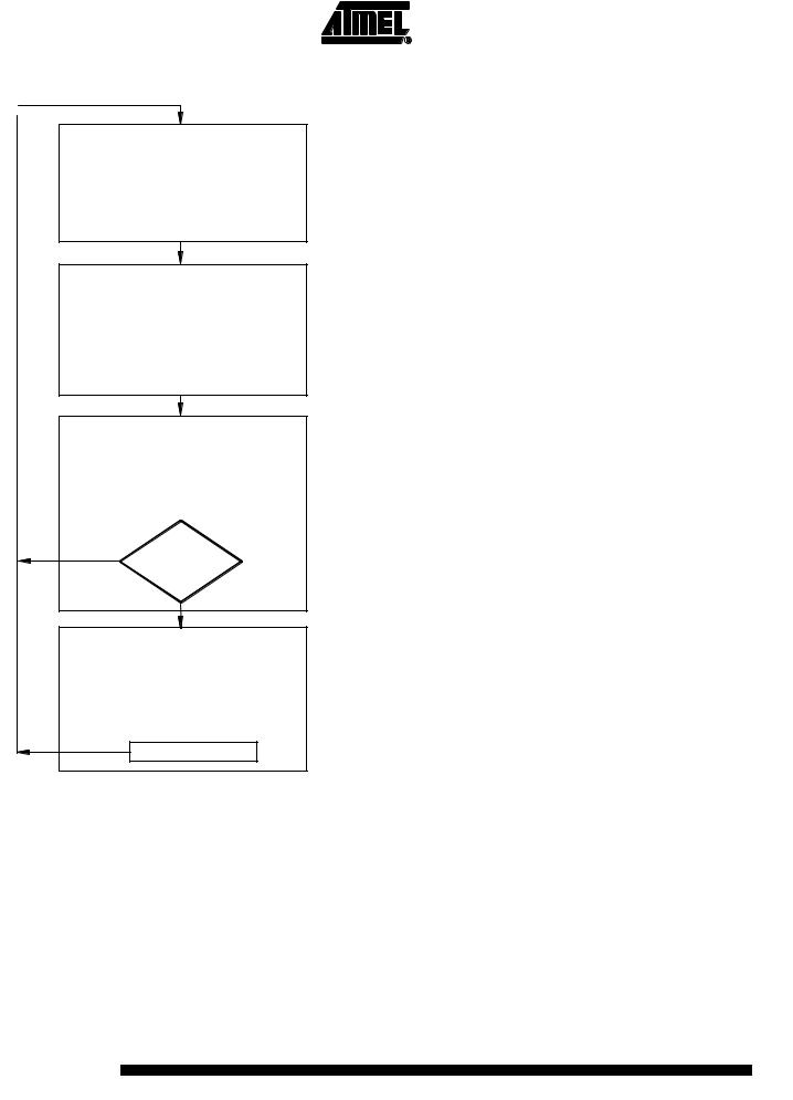
Figure 10. Polling Mode Flow Chart
Sleep mode:
All circuits for signal processing are disabled. Only XTO and Polling logic is enabled.
Output level on Pin IC_ACTIVE => low
IS = ISoff
TSleep = Sleep XSleep 1024 TClk
Start-up mode:
The signal processing circuits are
enabled. After the start-up time (TStartuprt ) all circuits are in stable
condition and ready to receive.
Output level on Pin IC_ACTIVE => high
IS = ISon
TStartup
Bit-check mode:
The incomming data stream is analyzed. If the timing indicates a valid transmitter signal, the receiver is set to receiving mode. Otherwise it is set to Sleep mode.
Output level on Pin IC_ACTIVE => high
|
IS = ISon |
|
|
TBit-check |
Bit-check |
|
|
|
NO |
|
OK ? |
YES
Receiving mode:
The receiver is turned on permanently and passes the data stream to the connected microcontrollerC. .
It can be set to Sleep mode through an OFF command via Pin DATA or POLLING/_ON.
Output level on Pin IC_ACTIVE => high
IS = ISon
|
|
|
|
|
|
|
|
|
|
|
|
|
|
|
|
|
|
Sleep:: |
5--bititworddefined byy Sleep0 to |
||||
|
|
|
|
Sleep4 inOPMODE registeri |
t r |
XSleep:: |
Extensioni factorr defined by |
||||
|
|
|
|
XSleepStd accordingtoTable9 |
|
TClk:: |
Basic clockck cycledefined by ffXTO |
||||
|
|
|
|
and PinMODE |
|
TStartup:: |
Isdefined byy the selectedl ct |
baud ratete |
|||
|
|
|
|
range and TClk..Thebaud-rate- rangeisis |
|
|
|
|
|
Clk |
|
|
|
|
|
defined byy Baud0 and Baud1 inthe |
|
OPMODE registerist r..
TBit--check:: Dependsnds ontheresultofthebitcheck..
IfIfthebitcheck is ok,TBitBit--checkdependsonthe numberberofbits tobechecked(NBitBit-check- ))andon theutilizeddatarate..
IfIfthebitcheckck fails,the averageragetime period forthatatcheck dependsnds ontheselectedlectedbaud--
raterangeandonTClk..Thebaud--raterangeisis definedby Baud0andBaud1intheOPMODE register
12 T5743
4569A–RKE–12/02
T5743
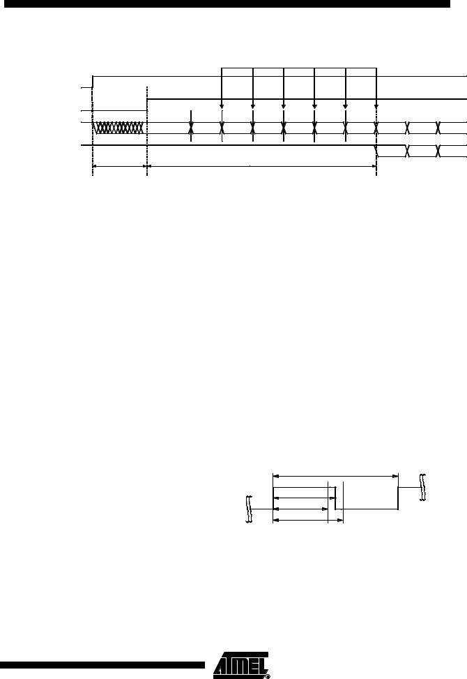
Figure 11. Timing Diagram for Complete Successful Bit Check
( Number of checked Bits: 3 ) |
Bit check ok |
|
|
IC_ACTIVE |
|
|
|
Bit check |
1/2 Bit |
1/2 Bit 1/2 Bit 1/2 Bit 1/2 Bit |
1/2 Bit |
|
|||
Dem_out |
|
|
|
Data_out (DATA) |
TStart-up |
TBit-check |
|
|
|
||
|
Start-up mode |
Bit-check mode |
Receiving mode |
Bit-check Mode
Configuring the Bit Check
In bit-check mode the incoming data stream is examined to distinguish between a valid signal from a corresponding transmitter and signals due to noise. This is done by subsequent time frame checks where the distances between two signal edges are continuously compared to a programmable time window. The maximum count of this edge-to-edge tests before the receiver switches to receiving mode is also programmable.
Assuming a modulation scheme that contains two edges per bit, two time frame checks are verifying one bit. This is valid for Manchester, Bi-phase and most other modulation schemes. The maximum count of bits to be checked can be set to 0, 3, 6 or 9 bits via the
variable NBit-check in the OPMODE register. This implies 0, 6, 12 and 18 edge to edge checks respectively. If NBit-check is set to a higher value, the receiver is less likely to
switch to receiving mode due to noise. In the presence of a valid transmitter signal, the
bit check takes less time if NBit–check is set to a lower value. In polling mode, the bit-check time is not dependent on NBit-check. Figure 11 shows an example where 3 bits are tested successfully and the data signal is transferred to Pin DATA.
According to Figure 12, the time window for the bit check is defined by two separate
time limits. If the edge-to-edge time tee is in between the lower bit-check limit TLim_min and the upper bit-check limit TLim_max, the check will be continued. If tee is smaller than
TLim_min or tee exceeds TLim_max, the bit check will be terminated and the receiver switches to sleep mode.
Figure 12. Valid Time Window for Bit Check
|
1/fSig |
|
Dem_out |
tee |
|
TLim_min |
||
|
||
|
TLim_max |
For best noise immunity it is recommended to use a low span between TLim_min and TLim_max. This is achieved using a fixed frequency at a 50% duty cycle for the transmitter preburst. A “11111...” or a “10101...” sequence in Manchester or Bi-phase is a good choice concerning that advice. A good compromise between receiver sensitivity and susceptibility to noise is a time window of ±25% regarding the expected edge-to-edge time tee. Using pre-burst patterns that contain various edge-to-edge time periods, the bit-check limits must be programmed according to the required span.
The bit-check limits are determined by means of the formula below.
13
4569A–RKE–12/02
 Loading...