


ANPEC APL5503-34VC-TR, APL5503-34UC-TR, APL5503-34KC-TR, APL5503-34DC-TR, APL5503-34BC-TR Datasheet
...APL5501/2/3
Low IQ, Low Dropout 500mA Fixed Voltage Regulator
Features
•Low Noise : 50 VRMS (100Hz to 100kHz)
•Low Quiescent Current : 50 A (No load)
•Low Dropout Voltage : 170mV (@500mA)
•Very low Shutdown Current : < 0.5uA
•Fixed Output Voltage : 1.3V ~ 3.4V
•Stable with 4.7uF Output Capacitor
•Stable with Aluminum , Tantalum or Ceramic Capacitors .
•Reverse Current Protection
•No Protection Diodes Needed
•Built in Thermal Protection
•Built in Current Limit Protection
•Controlled Short Circuit Current : 150mA
•Fast Transient Response
•Short Setting Time
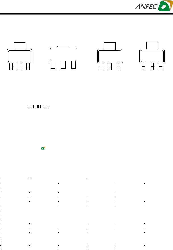
•SOT-23-5, SOT-89, SOT-89-5, SOT-223, SO-8 ,TO-252 and TO-252-5 Packages
Applications
•Notebook Computer
•PDA or Portable Equipments
•Noise-Sensitive Instrumentation Systems
Design with an internal P-channel MOSFET pass transistor, the APL5501/2/3 maintains a low supply current, independent of the load current and dropout voltage. Other features include reverse current protection, thermal-shutdown protection, current limit protection to ensure specified output current and controlled short-circuit current. The APL5501/2/3 regulator comes in a miniature SOT-23-5, SOT-89, SOT- 89-5, SOT-223, SO-8, TO-252 and TO-252-5 packages.
Pin Configuration
APL5501
|
|
|
|
|
|
|
|
|
|
|
|
BP |
G ND |
SHDN |
|
|
||||||||
|
|
T A B is G N D |
|
|
|
|
|
|
|
|
|
|
|
|
|
|
|
|
|
|
||||
|
|
|
|
|
|
|
|
|
|
|
|
|
|
|
|
|
|
|
|
|
|
|
|
|
|
|
|
|
|
|
|
|
|
|
|
5 |
|
|
|
|
4 |
|
|
|
|
||||
|
|
1 |
2 |
|
|
3 |
|
|
1 |
|
2 |
|
3 |
|
|
|
|
|||||||
|
|
|
|
|
|
|
|
|
|
|
|
|
|
|
|
|
||||||||
|
|
|
|
|
|
|
|
|
|
|
|
|
|
|
|
|
|
|
|
|
|
|
||
|
|
|
|
|
|
|
|
|
|
|
|
|
|
|
|
|
|
|
|
|
|
|
|
|
|
|
|
|
|
|
|
|
|
|
|
|
|
|
|
||||||||||
|
|
V IN |
G N D |
V O U T |
VOUT G ND VIN |
|
|
|||||||||||||||||
SOT-89 (Top View) |
SOT-89-5 (Top View) |
|||||||||||||||||||||||
|
|
|
|
|
|
|
|
|
|
|
|
|
|
|
|
|
|
|
|
|
|
|
|
|
IN |
|
1 |
|
|
8 |
|
|
|
OU T |
V IN |
|
|
|
1 |
|
|
5 |
|
|
|
VO U T |
|||
|
|
|
|
|
|
|
|
|
|
|
|
|
|
|||||||||||
G ND |
|
2 |
|
|
7 |
|
|
|
GN D |
|
|
|
|
|
|
|
|
|
|
|
|
|
|
|
|
|
|
|
|
|
|
|
|
|
|
|
|
|
|
|
|
|
|
|
|||||
G ND |
|
3 |
|
|
6 |
|
|
|
GN D |
G ND |
|
|
2 |
|
|
|
|
|
|
|
|
|
||
|
|
|
|
|
|
|
|
|
|
|
|
|
|
|
|
|
|
|
|
|||||
|
|
|
|
|
|
|
|
|
|
|
|
|
|
|
|
|
|
|
|
|
|
|
|
|
SHDN |
|
4 |
|
|
5 |
|
|
|
BYP |
SHDN |
|
|
|
3 |
|
|
4 |
|
|
|
BP |
|||
|
|
|
|
|
|
|
|
|
|
|
|
|
|
|
|
|
|
|
|
|
|
|
|
|
General Description
SO-8 (Top View) |
SOT-23-5 (Top View) |
The APL5501/2/3 is micropower, low noise, low dropout linear regulator. Operate from 2.7V to 6V input voltage and deliver up to 500mA. Typical output noise
is just 50 VRMS with the addition of an external 0.1 F bypass capacitor in BP pin and typical dropout volt-
age is only 170mV at 500mA loading . Designed for use in battery-powered system, the low 50uA quiescent current makes it an ideal choice.
GND
1 2 3
VIN VOUT
TABis GND

5 |
|
|
|
VOUT |
||
|
|
|
||||
|
|
|
|
|||
4 |
|
|
|
BP |
||
|
|
|
||||
3 |
|
|
|
GND |
||
|
|
|
||||
|
|
|
|
|
|
|
2 |
|
|
|
|
SHDN |
|
1 |
|
|
|
VIN |
||
|
|
|
||||
|
|
|
|
|
|
|
TO-252 (Top View) |
TO-252-5 (Top View) |
ANPEC reserves the right to make changes to improve reliability or manufacturability without notice, and advise customers to obtain the latest version of relevant information to verify before placing orders.
Copyright ANPEC Electronics Corp. |
1 |
www.anpec.com.tw |
Rev. A.9 - May., 2003 |
|
|
APL5501/2/3
Pin Configuration (Cont.)
|
|
APL5501 |
|
|
|
|
|
|
|
|
|
|
|
|
|
|
|
|
APL5502 |
|
|
|
|
|
APL5502 |
|
|
APL5503 |
|||||||||||||||
|
|
TAB is GND |
|
|
|
|
|
|
|
|
|
|
|
|
|
|
|
|
|
|
TAB is VIN |
|
TAB is GND |
||||||||||||||||||||
|
|
|
|
|
|
|
|
|
|
|
|
|
|
|
|
|
|
|
|
|
|
TAB is VIN |
|
|
|
|
|
|
|
|
|
|
|
|
|
|
|
|
|
|
|||
|
|
|
|
|
|
|
|
|
|
|
|
|
|
|
|
|
|
|
|
|
|
|
|
|
|
|
|
|
|
|
|
|
|
|
|
|
|
|
|
|
|
|
|
|
|
|
|
|
|
|
|
|
|
|
|
|
|
|
|
|
|
|
|
|
|
|
|
|
|
|
|
|
|
|
|
|
|
|
|
|
|
|
|
|
|
|
|
1 |
2 |
|
|
3 |
|
|
|
|
|
|
|
1 |
2 |
3 |
|
|
|
|
1 |
|
2 |
3 |
|
1 |
2 |
3 |
|
||||||||||||||||
|
|
|
|
|
|
|
|
|
|
|
|
|
|
|
|
|
|
|
|
|
|
|
|
|
|
|
|
||||||||||||||||
|
VIN G ND VOUT |
|
|
|
|
|
|
|
|
GND |
|
|
VIN |
VOUT |
GND |
VIN |
VOUT |
VOUT GND |
|
|
VIN |
||||||||||||||||||||||
|
SOT-223 (Top View) |
|
|
|
|
|
|
SOT-89 (Top View) |
SOT-223 (Top View) |
SOT-223 (Top View) |
|||||||||||||||||||||||||||||||||
Ordering and Marking Information |
|
|
|
|
|
|
|
|
|
|
|
||||||||||||||||||||||||||||||||
|
|
|
|
|
|
|
|
|
|
|
|
|
|
|
|
|
|
|
|
|
|
|
|
|
|
|
|
|
|
|
|
|
|
|
|
|
|
|
|
|
|
|
|
|
A P L 5 5 0 1 /2 /3 - |
|
|
|
|
|
|
|
|
|
|
|
|
|
|
|
|
|
|
|
|
|
|
|
|
|
P a c k a g e C o d e |
|
|
|
|
|
|
|
|
|
|
||||||
|
|
|
|
|
|
|
|
|
|
|
|
|
|
|
|
|
|
|
|
|
|
|
|
|
|
B : S O T -2 3 -5 |
D : S O T -8 9 |
|
|
D 5 : S O T -8 9 -5 |
|||||||||||||
|
|
|
|
|
|
|
|
|
|
|
|
|
|
|
|
|
|
|
|
|
|
|
|
|
|
|
|
|
|
|
|
|
|||||||||||
|
|
|
|
|
|
|
|
|
|
|
|
|
|
|
|
|
|
|
|
|
|
|
|
|
|
|
|
|
|
|
U : T O -2 5 2 |
U 5 : T O -2 5 2 -5 |
|
|
|
V : S O T -2 2 3 |
|||||||
|
|
|
|
|
|
|
|
|
|
|
|
|
|
|
|
|
|
|
|
|
|
|
|
H a n d lin g C o d e |
|
K : S O -8 |
|
|
|
|
|
|
|
|
|
|
|
||||||
|
|
|
|
|
|
|
|
|
|
|
|
|
|
|
|
|
|
|
|
|
|
|
|
|
|
|
|
|
|
|
|
|
|
|
|
||||||||
|
|
|
|
|
|
|
|
|
|
|
|
|
|
|
|
|
|
|
|
|
|
|
|
|
|
|
|
|
|
|
T e m p . R a n g e |
|
|
|
|
|
|
|
|
|
|
||
|
|
|
|
|
|
|
|
|
|
|
|
|
|
|
|
|
|
|
|
|
|
|
|
T e m p . R a n g e |
|
C : 0 to 7 0 |
°C |
|
|
|
|
|
|
|
|
|
|
||||||
|
|
|
|
|
|
|
|
|
|
|
|
|
|
|
|
|
|
|
|
|
|
|
|
|
|
|
|
|
|
|
|
|
|
|
|||||||||
|
|
|
|
|
|
|
|
|
|
|
|
|
|
|
|
|
|
|
|
|
|
|
|
P a c k a g e C o d e |
|
|
H a n d lin g C o d e |
|
|
|
|
|
|
|
|
|
|
||||||
|
|
|
|
|
|
|
|
|
|
|
|
|
|
|
|
|
|
|
|
|
|
|
|
|
|
T R : T a p e & R e e l |
|
|
|
|
|
|
|
|
|
|
|||||||
|
|
|
|
|
|
|
|
|
|
|
|
|
|
|
|
|
|
|
|
|
|
|
|
V o lta g e C o d e |
|
|
|
|
|
|
|
|
|
|
|
|
|||||||
|
|
|
|
|
|
|
|
|
|
|
|
|
|
|
|
|
|
|
|
|
|
|
|
|
V o lta g e C o d e : |
|
|
|
|
|
|
|
|
|
|
||||||||
|
|
|
|
|
|
|
|
|
|
|
|
|
|
|
|
|
|
|
|
|
|
|
|
|
|
|
|
|
|
|
|
|
|
|
|
||||||||
|
|
|
|
|
|
|
|
|
|
|
|
|
|
|
|
|
|
|
|
|
|
|
|
|
|
|
|
|
|
|
|
|
|
|
|
|
|
|
|
|
|||
|
|
|
|
|
|
|
|
|
|
|
|
|
|
|
|
|
|
|
|
|
|
|
|
|
|
|
|
|
|
|
1 3 : 1 .3 V ~ 3 4 : 3 .4 V |
|
|
|
|
|
|
|
|
||||
|
|
|
|
|
|
|
|
|
|
|
|
|
|
|
|
|
|
|
|
|
|
|
|
|
|
|
|
|
|
|
|
|
|
|
|
|
|
|
|
|
|
|
|
|
|
|
|
|
|
|
|
|
|
|
|
|
|
|
|
|
|
|
|
|
|
|
|
|
|
|
|
|
|
|
|
|
|
|
|
|
|
|
|
|
|||
|
A P L 5 5 0 1 /2 /3 - 1 3 D /V /K : |
|
|
|
|
A P L 5 5 0 1 /2 /3 |
|
|
|
|
|
|
|
|
X X X X X - D a te C o d e , 1 3 - 1 .3 V |
|
|
|
|
|
|
|
|
||||||||||||||||||||
|
|
|
|
|
X X X X X 1 3 |
|
|
|
|
|
|
|
|
|
|
|
|
|
|
|
|
||||||||||||||||||||||
|
|
|
|
|
|
|
|
|
|
|
|
|
|
|
|
|
|
|
|
|
|
|
|
|
|
|
|
|
|
|
|
|
|
|
|
|
|
||||||
|
|
|
|
|
|
|
|
|
|
|
|
|
|
|
|
|
|
|
|
|
|
|
|
|
|
|
|
|
|
|
|
|
|
|
|
|
|
|
|
|
|
|
|
|
|
|
|
|
|
|
|
|
|
|
|
|
|
|
|
|
|
|
|
|
|
|
|
|
|
|
|
|
|
|
|
|
|
|
|
|
|
||||||
|
|
|
|
|
|
|
|
|
|
|
|
|
|
|
|
1 3 |
|
|
|
|
|
|
|
|
|
|
|
|
|
|
|
|
|
|
|
|
|
||||||
|
A P L 5 5 0 1 /2 /3 - 1 3 U : |
|
|
|
|
A P L 5 5 0 1 /2 /3 |
|
|
|
|
|
|
|
|
X X X X X - D a te C o d e , 1 3 - 1 .3 V |
|
|
|
|
|
|
|
|
||||||||||||||||||||
|
|
|
|
|
|
|
|
|
|
|
|
|
|
|
|
|
X X X X X |
|
|
|
|
|
|
|
|
|
|
|
|
|
|
|
|
|
|
|
|
|
|||||
|
|
|
|
|
|
|
|
|
|
|
|
|
|
|
|
|
|
|
|
|
|
|
|
|
|
|
|
|
|
|
|
|
|
|
|
|
|
|
|
|
|
|
|
Marking Information |
|
|
|
|
|
|
|
|
|
|
|
|
|
|
|
|
|
|
|
|
|
||||||||||||||||||||||
SOT-23-5 package |
|
|
|
|
|
|
|
|
|
|
|
|
|
|
|
|
|
|
|
|
|
|
|
|
|
|
|
|
|
|
|
||||||||||||
|
|
|
|
|
|
|
|
|
|
|
|
|
|
|
|
|
|
|
|
|
|
|
|
|
|
|
|
|
|
|
|
|
|
|
|
|
|
||||||
|
Product Name |
|
|
|
|
Marking |
|
Product Name |
|
Marking |
Product Name |
|
|
Marking |
|||||||||||||||||||||||||||||
|
APL5501-13B |
|
|
|
|
|
|
|
|
|
|
517X |
|
|
APL5502-13B |
|
527X |
|
APL5503-13B |
|
|
537X |
|||||||||||||||||||||
|
APL5501-14B |
|
|
|
|
|
|
|
|
|
|
518X |
|
|
APL5502-14B |
|
528X |
|
APL5503-14B |
|
|
538X |
|||||||||||||||||||||
|
APL5501-15B |
|
|
|
|
|
|
|
|
|
|
519X |
|
|
APL5502-15B |
|
529X |
|
APL5503-15B |
|
|
539X |
|||||||||||||||||||||
|
APL5501-16B |
|
|
|
|
|
|
|
|
|
|
51AX |
|
|
APL5502-16B |
|
52AX |
|
APL5503-16B |
|
|
53AX |
|||||||||||||||||||||
|
APL5501-17B |
|
|
|
|
|
|
|
|
|
|
51BX |
|
|
APL5502-17B |
|
52BX |
|
APL5503-17B |
|
|
53BX |
|||||||||||||||||||||
|
APL5501-18B |
|
|
|
|
|
|
|
|
|
|
51CX |
|
|
APL5502-18B |
|
52CX |
|
APL5503-18B |
|
|
53CX |
|||||||||||||||||||||
|
APL5501-19B |
|
|
|
|
|
|
|
|
|
|
51DX |
|
|
APL5502-19B |
|
52DX |
|
APL5503-19B |
|
|
53DX |
|||||||||||||||||||||
|
APL5501-20B |
|
|
|
|
|
|
|
|
|
|
51EX |
|
|
APL5502-20B |
|
52EX |
|
APL5503-20B |
|
|
53EX |
|||||||||||||||||||||
|
APL5501-21B |
|
|
|
|
|
|
|
|
|
|
51FX |
|
|
APL5502-21B |
|
52FX |
|
APL5503-21B |
|
|
53FX |
|||||||||||||||||||||
|
APL5501-22B |
|
|
|
|
|
|
|
|
|
51GX |
|
|
APL5502-22B |
|
52GX |
APL5503-22B |
|
|
53GX |
|||||||||||||||||||||||
|
APL5501-23B |
|
|
|
|
|
|
|
|
|
|
51HX |
|
|
APL5502-23B |
|
52HX |
|
APL5503-23B |
|
|
53HX |
|||||||||||||||||||||
|
APL5501-24B |
|
|
|
|
|
|
|
|
|
|
51IX |
|
|
APL5502-24B |
|
52IX |
|
APL5503-24B |
|
|
|
53IX |
||||||||||||||||||||
|
APL5501-25B |
|
|
|
|
|
|
|
|
|
|
51JX |
|
|
APL5502-25B |
|
52JX |
|
APL5503-25B |
|
|
53JX |
|||||||||||||||||||||
|
APL5501-26B |
|
|
|
|
|
|
|
|
|
|
51KX |
|
|
APL5502-26B |
|
52KX |
|
APL5503-26B |
|
|
53KX |
|||||||||||||||||||||
|
APL5501-27B |
|
|
|
|
|
|
|
|
|
|
51LX |
|
|
APL5502-27B |
|
52LX |
|
APL5503-27B |
|
|
53LX |
|||||||||||||||||||||
|
|
|
|
|
|
|
|
|
|
|
|
|
|
|
|
|
|
|
|
|
|
|
|
|
|
|
|
|
|
|
|
|
|
|
|
|
|
|
|
|
|
|
|
Copyright ANPEC Electronics Corp. |
|
|
|
2 |
|
|
|
|
|
|
www.anpec.com.tw |
||||||||||||||||||||||||||||||||
Rev. A.9 - May., 2003 |
|
|
|
|
|
|
|
|
|
|
|
|
|
|
|
|
|
|
|
|
|
|
|
|
|
|
|
|
|
|
|
||||||||||||

APL5501/2/3
Marking Information (Cont.)
SOT-23-5 package
Product Name |
Marking |
Product Name |
Marking |
Product Name |
Marking |
APL5501-28B |
51MX |
APL5502-28B |
52MX |
APL5503-28B |
53MX |
APL5501-29B |
51NX |
APL5502-29B |
52NX |
APL5503-29B |
53NX |
APL5501-30B |
51OX |
APL5502-30B |
52OX |
APL5503-30B |
53OX |
APL5501-31B |
51PX |
APL5502-31B |
52PX |
APL5503-31B |
53PX |
APL5501-32B |
51QX |
APL5502-32B |
52QX |
APL5503-32B |
53QX |
APL5501-33B |
51RX |
APL5502-33B |
52RX |
APL5503-33B |
53RX |
APL5501-34B |
51SX |
APL5502-34B |
52SX |
APL5503-34B |
53SX |
The last character “X” in the marking is for data code.
Pin Description
|
|
PIN |
I/O |
Description |
|
No. |
|
Name |
|||
|
|
|
|||
1 |
|
VIN |
I |
Supply voltage input. |
|
2 |
|
|
(Note1) |
I |
Shutdown control pin, low = off , high = normal . |
|
SHDN |
||||
3 |
|
GND |
|
Ground pins of the circuitry, and all ground pins must be soldered to |
|
|
|
PCB with proper power dissipation. |
|||
|
|
|
|
|
|
|
|
|
|
|
|
4 |
|
BP(Note1) |
O |
Bypass signal pin in fixed output type device |
|
5 |
|
VOUT |
O |
Output pin of the regulator. |
|
|
|
|
|
|
|
Note1 : These pins do not exist in 3-pin package.
Absolute Maximum Ratings
Symbol |
Parameter |
Rating |
Unit |
|||
VIN, VOUT |
Input Voltage or Out Voltage |
5 |
V |
|||
|
|
|
|
|
|
|
|
|
|
Shutdown Control Pin |
|
|
|
SHDN |
5 |
V |
||||
|
||||||
|
|
|
|
|
|
|
|
|
|
|
SOT-89 : 180 |
|
|
RTH,JA |
Thermal Resistance – Junction to Ambient |
SOT-223 : 135 |
°C/W |
|||
SO-8 : 210 |
||||||
|
|
|
|
|
||
|
|
|
|
SOT-23-5 : 357 |
|
|
|
PD |
Power Dissipation |
Internally Limited |
W |
||
|
|
|
|
|
|
|
|
TJ |
Operating Junction Temperature |
|
°C |
||
|
|
|
Control Section |
0 to 125 |
|
|
|
|
|
Power Transistor |
0 to 150 |
|
|
|
|
|
|
|
|
|
|
TSTG |
Storage Temperature Range |
-65 to +150 |
°C |
||
|
TL |
Lead Temperature (Soldering, 10 second) |
260 |
°C |
||
|
|
|
|
|
|
|
Copyright ANPEC Electronics Corp. |
3 |
www.anpec.com.tw |
Rev. A.9 - May., 2003 |
|
|

APL5501/2/3
Electrical Characteristics
Unless otherwise noted these specifications apply over full temperature, VIN=3.6V, CIN=1 F, COUT=4.7 F, SHDN=VIN, TJ=0 to 125°C. Typical values refer to TJ=25°C.
Symbol |
Parameter |
|
|
Test Conditions |
APL5501/2/3 |
Unit |
|||||
|
|
|
|
|
|||||||
Min. |
Typ. |
Max. |
|||||||||
|
|
|
|
|
|
|
|
||||
|
|
|
|
|
|
|
|
|
|
|
|
|
VIN |
Input Voltage |
|
|
|
2.7 |
|
6 |
V |
||
VOUT |
Output Voltage |
VOUT+1.0V< VCC<6.0V, 0mA< IOUT < IMAX |
VOUT -2% |
VOUT |
VOUT +2% |
V |
|||||
ILIMIT |
Circuit Current Limit |
VIN=4.3V |
|
0.7 |
|
A |
|||||
ISHORT |
Short Current |
VOUT=0V |
|
200 |
|
mA |
|||||
IOUT |
Load Current |
|
|
|
500 |
|
|
mA |
|||
REGLINE |
Line Regulation |
VOUT+0.5V< VCC<6.0V, 0mA< IOUT < IMAX |
|
4 |
10 |
mV |
|||||
REGLOAD |
Load Regulation |
VIN =VOUT+1.0V, 0mA< IOUT < IMAX |
|
1 |
6 |
mV |
|||||
|
|
|
Dropout Voltage(Note2) |
IOUT =500mA |
|
|
|
|
|||
VDROP |
(VOUT(Nominal)=3.0V |
|
170 |
300 |
mV |
||||||
|
|
|
|
||||||||
|
|
|
Version) |
|
|
|
|
|
|
|
|
|
|
|
|
|
|
|
|
|
|
|
|
PSRR |
Ripple Rejection |
F≤1kHz, 1Vpp at VIN = VOUT+1.0V |
55 |
65 |
|
dB |
|||||
|
IQ |
Quiescent Current |
No load |
|
50 |
100 |
A |
||||
|
|
|
|
|
|
|
|||||
IOUT=500mA |
|
370 |
450 |
||||||||
|
|
|
|
|
|
||||||
|
|
|
|
|
|
|
|
|
|
|
|
|
|
|
Shutdown Supply |
Shutdown = low |
|
0.01 |
1 |
A |
|||
|
|
|
Current(Note3) |
IOUT=0, VCC =6.0V |
|
||||||
|
|
|
|
|
|
|
|||||
|
|
|
|
|
|
|
|
|
|
|
|
|
|
|
|
100Hz<f<100kHz, typical load, |
|
50 |
|
|
|||
|
|
|
|
CBP=0.01 F, COUT = 1 F |
|
|
|
||||
|
|
|
Noise(Note3) |
|
|
|
Vrms |
||||
|
|
|
100Hz<f<100kHz, typical load, |
|
40 |
|
|||||
|
|
|
|
|
|
|
|||||
|
|
|
|
CBP=0.1 F, COUT = 1 F |
|
|
|
||||
|
|
|
|
|
|
|
|
||||
|
|
|
|
|
|
|
|
|
|
|
|
|
|
|
Shutdown Recovery |
CBP=0.01 F,COUT=1 F, no load |
|
7 |
|
ms |
|||
|
|
|
Delay(Note3) |
CBP=0.1 F,COUT=1 F, no load |
|
70 |
|
||||
|
|
|
|
|
|
||||||
OTS |
Over Temperature |
|
|
|
|
150 |
|
°C |
|||
Shutdown |
|
|
|
|
|
||||||
|
|
|
|
|
|
|
|
|
|
||
|
|
|
|
|
|
|
|
|
|
|
|
|
|
|
Over Temperature |
Hysteries |
|
10 |
|
°C |
|||
|
|
|
Shutdown Hysteresis |
|
|
||||||
|
|
|
|
|
|
|
|
|
|
||
|
|
|
|
|
|
|
|
|
|
|
|
|
|
|
Output Voltage |
|
|
|
|
|
|
|
|
|
TC |
Temperature |
|
|
|
|
50 |
|
ppm/°C |
||
|
|
|
Coefficient |
|
|
|
|
|
|
|
|
|
|
|
|
|
|
|
|
|
|
|
|
COUT |
Output Capacitor |
|
|
|
4.2 |
4.7 |
5.2 |
F |
|||
|
|
|
ESR |
|
|
|
0.02 |
0.1 |
1 |
Ohm |
|
|
|
|
|
|
|
|
|
|
|
|
|
|
|
|
Shutdown Input |
VOUT+1.0V< VIN <6.0V |
0.4 |
0.7 |
1.6 |
V |
|||
|
|
|
Threshold(Note3) |
||||||||
I |
|
|
Shutdown input Bias |
V |
|
=VIN |
|
0.01 |
100 |
nA |
|
SHDN |
|
current(Note3) |
|
|
|||||||
|
SHDN |
|
|||||||||
|
|
|
Input Reverse Leakage |
VOUT-VIN=0.1V |
|
0.1 |
0.5 |
A |
|||
|
|
|
current |
|
|
|
|
|
|
|
|
|
|
|
Reverse Protection |
|
|
|
|
11 |
50 |
mV |
|
|
|
|
Threshold |
|
|
|
|
||||
|
|
|
|
|
|
|
|
|
|
||
|
|
|
|
|
|
|
|
|
|
|
|
Note 2 : Dropout voltage definition : VIN-VOUT when VOUT is 2% below the value of VOUT for VIN = VOUT + 0.5V Note 3 : For 5-pin devices only.
Copyright ANPEC Electronics Corp. |
4 |
www.anpec.com.tw |
Rev. A.9 - May., 2003 |
|
|
APL5501/2/3
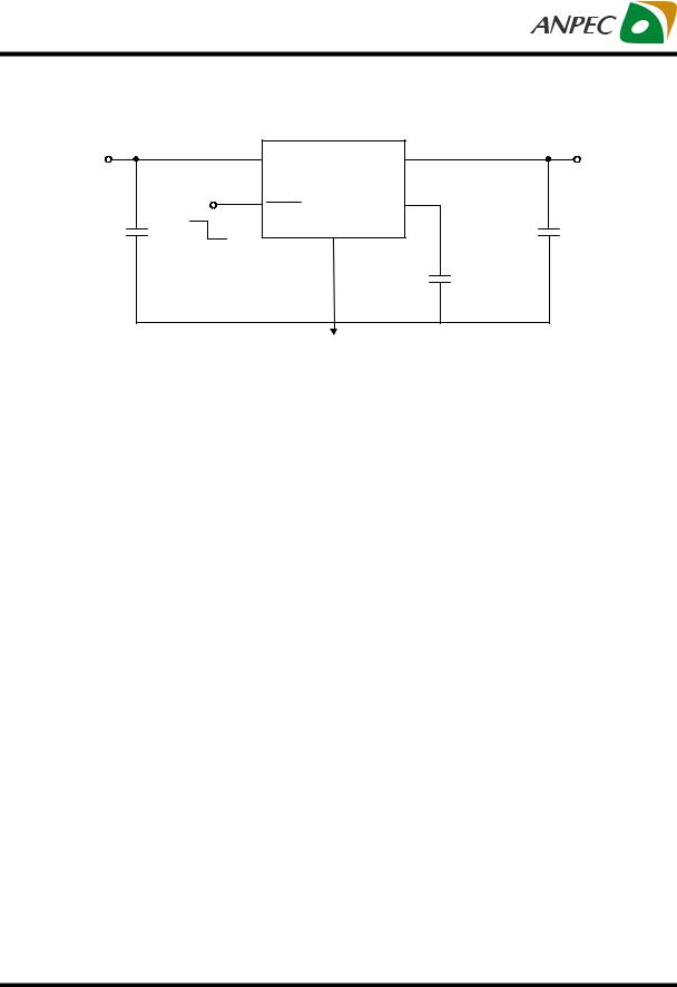
Application Circuit
INPUT |
|
VIN |
VO U T |
VO U T |
2.7V to 6V |
|
|
|
|
|
|
APL5501/2/3 |
|
|
|
on |
SH D N |
BP |
|
|
|
|
||
CIN |
G N D |
|
C O U T |
|
|
|
|||
1uF |
|
off |
|
4.7uF |
|
|
|
|
|
|
|
|
CBP |
0.1uF |
Copyright ANPEC Electronics Corp. |
5 |
www.anpec.com.tw |
Rev. A.9 - May., 2003 |
|
|
APL5501/2/3
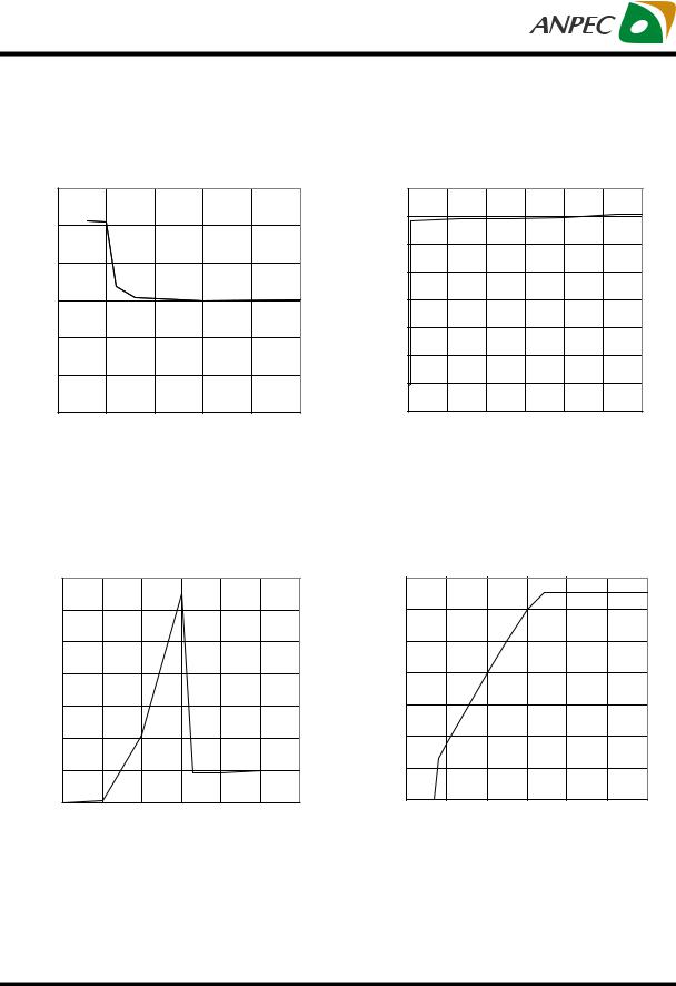
Typical Characteristics
Current Limit vs. Input Voltage
|
3 |
|
|
|
APL5501/2/3-33 |
|
|
|
|
|
|
|
|
|
2.5 |
|
|
|
|
|
(mA) |
2 |
|
|
|
|
|
|
|
|
|
|
|
|
Limit |
1.5 |
|
|
|
|
|
|
|
|
|
|
|
|
Current |
1 |
|
|
|
|
|
|
|
|
|
|
|
|
|
0.5 |
|
|
|
|
|
|
0 |
|
|
|
|
|
|
3.5 |
4 |
4.5 |
5 |
5.5 |
6 |
Input Voltage (V)
(uA) |
|
Ground Pin Current vs. Input Voltage |
|||||
350 |
|
|
|
|
APL5501/2/3-33 |
||
|
|
|
|
|
|
||
Current |
300 |
|
|
|
|
|
|
250 |
|
|
|
|
|
|
|
Load |
|
|
|
|
|
|
|
200 |
|
|
|
|
|
|
|
vs. |
|
|
|
|
|
|
|
|
|
|
|
|
|
|
|
Current |
150 |
|
|
|
|
|
|
100 |
|
|
|
|
|
|
|
Pin |
50 |
|
|
|
|
|
|
Ground |
|
|
|
|
|
|
|
0 |
|
|
|
|
|
|
|
0 |
1 |
2 |
3 |
4 |
5 |
6 |
|
Input Voltage (V)
Ground Pin Current vs. Output Current
(uA) |
400 |
|
|
|
|
APL5501/2/3-33 |
|
|
|
|
|
|
|
||
|
|
|
|
|
|
|
|
Current |
350 |
|
|
|
|
|
|
300 |
|
|
|
|
|
|
|
Load |
250 |
|
|
|
|
|
|
|
|
|
|
|
|
|
|
vs. |
200 |
|
|
|
|
|
|
|
|
|
|
|
|
|
|
Current |
150 |
|
|
|
|
|
|
100 |
|
|
|
|
|
|
|
Pin |
50 |
|
|
|
|
|
|
Ground |
|
|
|
|
|
|
|
0 |
|
|
|
|
|
|
|
0 |
150 |
300 |
450 |
600 |
750 |
900 |
|
|
|
|
|
|
|
|
|
Output Current (mA)
Input Voltage vs. Output Voltage
|
3.5 |
|
|
|
|
APL5501/2/3-33 |
|
|
|
|
|
|
|
|
|
|
3 |
|
|
|
|
|
|
(V) |
2.5 |
|
|
|
|
|
|
|
|
|
|
|
|
|
|
Voltage |
2 |
|
|
|
|
|
|
1.5 |
|
|
|
|
|
|
|
Output |
|
|
|
|
|
|
|
1 |
|
|
|
|
|
|
|
|
|
|
|
|
|
|
|
|
0.5 |
|
|
|
|
|
|
|
0 |
|
|
|
|
|
|
|
0 |
1 |
2 |
3 |
4 |
5 |
6 |
Input Voltage (V)
Copyright ANPEC Electronics Corp. |
6 |
www.anpec.com.tw |
Rev. A.9 - May., 2003 |
|
|

APL5501/2/3
Typical Characteristics
Dropout Voltage vs. Output Current
|
250 |
|
|
|
|
APL5501/2/3-33 |
|
|
|
|
|
|
|
|
|
(mV) |
200 |
|
|
|
|
|
|
|
|
|
|
|
|
|
|
Voltage |
150 |
|
|
|
|
|
|
100 |
|
|
|
|
|
|
|
Dropout |
|
|
|
|
|
|
|
50 |
|
|
|
|
|
|
|
|
|
|
|
|
|
|
|
|
0 |
|
|
|
|
|
|
|
0 |
150 |
300 |
450 |
600 |
750 |
900 |
Output Current (mA)
SHDN Threshold Voltage vs. Input Voltage
|
1 |
|
|
|
|
APL5501/2/3-33 |
|
|
|
|
|
|
|
|
|
(V) |
0.9 |
|
|
|
|
|
|
|
|
|
|
|
|
|
|
Voltage |
0.8 |
|
|
VIN=0V |
|
|
|
|
|
|
|
|
|
||
|
|
|
|
|
|
|
|
Threshold |
0.7 |
|
|
|
|
|
|
0.6 |
|
|
|
|
|
|
|
|
|
|
|
|
|
|
|
SHDN |
0.5 |
|
|
|
|
|
|
|
|
|
|
|
|
|
|
|
0.4 |
|
|
|
|
|
|
|
3 |
3.5 |
4 |
4.5 |
5 |
5.5 |
6 |
Input Voltage (V)
Output Current vs. Output Voltage
|
0 |
|
|
|
|
|
APL5501/2/3-33 |
|
|
|
|
|
|
|
|
|
-2 |
|
|
|
|
|
|
(uA) |
-4 |
|
|
|
VIN=0V |
|
|
Current |
|
|
|
|
|
||
|
|
|
|
|
|
||
-6 |
|
|
|
|
|
|
|
|
|
|
|
|
|
|
|
Output |
-8 |
|
|
|
|
|
|
|
|
|
|
|
|
|
|
|
-10 |
|
|
|
|
|
|
|
-12 |
|
|
|
|
|
|
|
0 |
0.5 |
1 |
1.5 |
2 |
2.5 |
3 |
Output Voltage (V)
PSRR vs. Frequency
PSRR (dB)
+0 |
|
|
|
|
|
|
-10 |
|
|
|
|
|
|
-20 |
|
|
|
|
|
|
-30 |
|
|
|
|
|
|
-40 |
|
|
IOUT =50mA |
|
||
-50 |
|
|
COUT=10uF |
|
||
|
|
CBP=0.1uF |
|
|||
-60 |
|
|
|
|
|
|
-70 |
|
|
|
|
|
|
-80 |
|
|
|
|
|
|
-90 |
|
|
|
|
|
|
-10020 |
50 |
100 |
200 |
500 |
1k |
2k |
APL5501/2/3-33
VIN=4V
VIN=5V
5k |
10k |
20k |
50k |
100k200k |
Frequency (HZ)
Copyright ANPEC Electronics Corp. |
7 |
www.anpec.com.tw |
Rev. A.9 - May., 2003 |
|
|
 Loading...