


ANPEC APL1431LBBI-TR, APL1431LBBI-TB, APL1431LBBI-PB, APL1431LBBC-TR, APL1431LBBC-TB Datasheet
...
APL1431L
Low Voltage Adjustable Precision Shunt Regulator
Features
•Precise Reference Voltage to 1.24V
•Guaranteed 0.5% or 1% Reference Voltage Tolerance
•Sink Current Capability , 60mA to 100mA
•Quick Turn-on
•Adjustable Output Voltage , VO = VREF to 20V
•Low Operational Cathode Current , 60mA Typical
•0.1Ω Typical Output Impedance
•SOT-23-5 Packages
Applications
•Linear Regulators
•Adjustable Power Supply
•Switching Power Supply
Symbol
REF
Anode |
Cathode |
General Description
The APL1431L is a 3-terminal low voltage adjustable precision reference with specified thermal stability over applicable commercial temperature ranges
. Output voltage may be set to any value between VREF (1.24 V) and 20 V with two external resistors (see Figure 2) . When used with an photocoupler , the APL1431L is an ideal voltage reference in isolated feedback circuits for 1.24V to 12V switchingmode power supplies . This device has a typical output impedance of 0.1Ω . Active output circuitry provides a very sharp turn-on characteristic , making the APL1431L excellent replacements for zener diodes in many applications , including on-board regulation and adjustable power supplies .
ANODE REF
5 4
1 2 3
NC NC CATHODE
Functional Diagram
|
Cathode |
REF |
+ |
|
− |
|
VREF |
|
Anode |
ANPEC reserves the right to make changes to improve reliability or manufacturability without notice, and advise customers to obtain the latest version of relevant information to verify before placing orders.
Copyright ANPEC Electronics Corp. |
1 |
www.anpec.com.tw |
Rev. A.4 - May., 2003 |
|
|

APL1431L
Ordering and Marking Information
APL1431L |
Elec. Grade |
|
||||||||||||||
|
|
|
|
|
|
|
|
|
|
|
|
|
|
|
|
|
|
|
|
|
|
|
|
|
|
|
|
|
|
|
|
A : 0.5% Reference Voltage Tolerance |
|
|
|
|
|
|
|
|
|
|
|
|
|
|
|
Handling Code |
B : 1% Reference Voltage Tolerance |
|
|
|
|
|
|
|
|
|
|
|
|
|
|
|
|||
|
|
|
|
|
|
|
|
|
|
|
|
|
|
Temp. Range |
Package Code |
|
|
|
|
|
|
|
|
|
|
|
|
|
|
|
B : SOT23 - 5 |
|
|
|
|
|
|
|
|
|
|
|
|
|
|
|
|
|
||
|
|
|
|
|
|
|
|
|
|
|
|
|
|
|
|
|
|
|
|
|
|
|
|
|
|
|
|
|
|
|
Package Code |
Temp. Range |
|
|
|
|
|
|
|
|
|
|
|
|
|
|
|
C : 0 to 70 C |
I : -40 to 85 C |
|
|
|
|
|
|
|
|
|
|
|
|
|
|
|
|
||
|
|
|
|
|
|
|
|
|
|
|
|
|
|
Elec. Grade |
Handling Code |
|
|
|
|
|
|
|
|
|
|
|
|
|
|
|
|
||
|
|
|
|
|
|
|
|
|
|
|
|
|
|
|
PB : Plastic Bag |
TB : Tape & Box |
|
|
|
|
|
|
|
|
|
|
|
|
|
|
|
TR : Tape & Reel |
|
|
|
|
|
|
|
|
|
|
|
|
|
|
|
|
|
|
|
|
|
|
|
||||||||||||
APL1431L B : |
1431L |
|
|
|
|
|
|
|||||||||
|
|
|
|
|
|
|
|
|
|
|
|
|
|
|
|
|
|
|
|
|
|
|
|
|
|
|
|
|
|
|
|
|
|
Absolute Maximum Ratings
Symbol |
|
Parameter |
|
|
|
Rating |
|
|
Unit |
|||
|
|
|
|
|
|
|
|
|
|
|
|
|
VKA |
|
Cathode Voltage |
|
|
|
|
20 |
|
|
|
V |
|
IK |
|
Continuous Cathode Current |
|
|
|
100 |
|
|
mA |
|||
IREF |
|
Reference Current |
|
|
|
|
3 |
|
|
mA |
||
JA |
|
Thermal Resistance from Junction to Ambient in Free Air |
|
|
357 |
|
|
C/W |
||||
θ |
|
|
|
SOT-23-5 |
|
|
|
|
° |
|
||
|
|
|
|
|
|
|
|
|
|
|
||
|
|
|
|
|
|
|
|
|
|
|
|
|
TJ |
|
Operating Junction Temperature Range |
|
|
-40 to 150 |
|
|
|
°C |
|||
TSTG |
Storage Temperature Range |
|
|
-65 to 150 |
|
|
|
°C |
||||
TSOL |
Lead Temperature Range, Ts (Soldering, 10sec) |
|
|
260 |
|
|
|
°C |
||||
Electrical Characteristics TA= 25°C ( unless otherwise noted) |
|
|
|
|
||||||||
|
|
|
|
|
|
|
|
|
|
|
||
Symbol |
|
Parameter |
Test Conditions |
|
APL1431L |
|
Unit |
|||||
|
Min. |
|
Typ. |
Max. |
|
|||||||
|
|
|
|
|
|
|
|
|||||
|
|
|
VKA=VREF, IK=10mA |
APL1431LA |
1.234 |
|
1.240 |
1.246 |
|
|
||
VREF |
Reference Voltage |
TA= 25°C, (Fig. 1) |
APL1431LB |
1.228 |
|
1.240 |
1.252 |
|
V |
|||
TA= full range |
APL1431LA |
1.222 |
|
1.240 |
1.258 |
|
||||||
|
|
|
(see Note 1), (Fig. 1) |
APL1431LB |
1.215 |
|
1.240 |
1.265 |
|
|
||
|
|
|
|
|
|
|
|
|
|
|
|
|
VDEV |
VDEF Temp Deviation |
TA= full range(see Note 1), |
|
|
|
5 |
15 |
|
mV |
|||
VKA =VREF , IK =10mA, (Fig. 1) |
|
|
|
|
||||||||
|
|
|
|
|
|
|
|
|
|
|
||
|
|
|
|
|
|
|
|
|
|
|
|
|
∆VREF |
Ratio of Change in VREF |
IK=10mA, ∆VKA =16V to VREF (Fig. 2) |
|
|
|
|
|
|
|
|
||
to Change in Cathode |
|
|
|
-0.2 |
-1.0 |
|
mV/V |
|||||
/∆VKA |
|
|
|
|
||||||||
Voltage |
|
|
|
|
|
|
|
|
|
|
||
|
|
|
|
|
|
|
|
|
|
|
||
|
|
|
|
|
|
|
|
|
|
|||
IREF |
Reference Input Current |
IK=10mA, R1=10kΩ, R2=∞ (Fig. 2) |
|
|
|
0.15 |
0.5 |
|
µA |
|||
|
|
|
|
|
|
|
|
|
|
|
|
|
Copyright ANPEC Electronics Corp. |
2 |
|
|
|
|
www.anpec.com.tw |
||||||
Rev. A.4 - May., 2003 |
|
|
|
|
|
|
|
|
|
|
||
APL1431L
Electrical Characteristics |
TA= 25°C ( unless otherwise noted) |
|
|
||||||||
|
|
|
|
|
|
|
|
|
|
|
|
Symbol |
Parameter |
|
Test Conditions |
|
|
APL1431L |
|
Unit |
|||
|
|
Min. |
|
Typ. |
|
Max. |
|||||
|
|
|
|
|
|
|
|
|
|||
|
|
|
|
|
|
|
|
|
|
||
IREF(DEV) |
IREF Temp Deviation |
TA= full range(see Note 1), R1=10kΩ, |
|
|
0.05 |
|
0.3 |
µA |
|||
R2=∞ , IK=10mA, (Fig. 2) |
|
|
|
|
|||||||
|
|
|
|
|
|
|
|
|
|||
IK(off) |
Off-state cathode current |
VREF=0V, (Fig. 3) |
|
VK=6V |
|
|
0.01 |
|
0.1 |
µA |
|
|
VK=16V |
|
|
0.01 |
|
0.5 |
|||||
|
|
|
|
|
|
|
|
|
|||
ZKA |
Dynamic Output |
VKA =VREF |
, IK=100µA to 100mA , |
|
|
0.1 |
|
0.3 |
Ω |
||
Impedance |
f<1kHz , (Fig. 1 ) |
|
|
|
|
||||||
|
|
|
|
|
|
|
|
||||
|
|
|
|
|
|
|
|
|
|
|
|
IK(MIN) |
Minimum Operating |
VKA =VREF , (Fig. 1) |
|
|
|
60 |
|
80 |
µA |
||
Current |
|
|
|
|
|||||||
|
|
|
|
|
|
|
|
|
|
|
|
|
|
|
|
|
|
|
|
|
|
|
|
Note : 1. Full temperature range is 0°C to 70°C for APL1431LXXC, and –40°C to 85°C for APL1431LXXI.
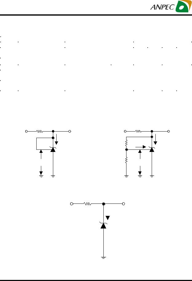
Test Circuits
VIN |
VO |
VIN |
VO |
|
I K |
|
I K |
|
|
R1 |
I REF |
|
V REF |
R2 |
VREF |
|
|
Figure 1. Test Circuit for VKA=VREF, VO=VKA=VREF |
Figure 2. Test Circuit for VKA>VREF, |
||||
|
|
|
|
|
VO= VKA= VREF× (1+R1/R2) + IREF × R1 |
VIN |
|
|
|
VO |
|
|
|
|
|
|
IK(OFF) |
|
|
|
|
|
|
|
|
|
|
|
|
|
|
|
|
|
|
Figure 3. Test Circuit for IK(OFF)
Copyright ANPEC Electronics Corp. |
3 |
www.anpec.com.tw |
Rev. A.4 - May., 2003 |
|
|
 Loading...