


a |
Serial-Port 16-Bit |
|
SoundComm Codec |
||
|
|
|
|
|
AD1843 |
|
|
|
FEATURES
Single Chip Integrated Speech, Audio, Fax and Modem Codec
Highly Configurable Stereo åD ADCs and Quad åD DACs
Supports V.34, V.32bis, and Fallback Modem Standards As Well As Voice Over Data
Dual Digital Resamplers with Programmable Input and Output Phase and Frequency
Three On-Chip Phase Lock Loops for Synchronization to External Signals, Including Video
Thirteen Analog Inputs and Seven Analog Outputs Advanced Analog and Digital Signal Mixing and Digital-
to-Digital Sample Rate Conversion Programmable Gain, Attenuation and Mute On-Chip Signal Filters
Digital Interpolation and Decimation Analog Output Low Pass
1 Hz Resolution Programmable Sample Rates from 4 kHz to 54 kHz Derived from a Single Clock Input
80-Lead PQFP and 100-Lead TQFP Packages Operation from +5 V or Mixed +5 V/+3 V Supplies FIFO-Buffered Serial Digital Interface Compatible with
ADSP-21xx Fixed-Point DSPs Advanced Power Management
VHDL Model of Serial Port Available; Evaluation Board and MAFE Board Available
GENERAL PRODUCT DESCRIPTION
The AD1843 SoundComm™ Codec is a complete analog front end for high performance DSP-based telephony and audio applications. The device integrates the real-world analog I/O requirements for many popular functions thereby reducing size, power consumption, and system complexity. The AD1843 SoundComm is the world’s first codec which can support four different sample rates simultaneously, without any beat frequency noise issues. This is essential for highly integrated audio/ modem/fax products since the sample rates associated with audio are very much distinct from the sample rates associated with telephony-oriented data communication. It is also the first codec to offer on-chip digital phase lock loops for sample rate synchronization to external clock signals. This sample rate flexibility is enabled through Analog Devices’ Continuous Time Oversampling (CTO) technology.
The main elements of the AD1843 are its extensive input and mixing section, its two channels of sigma-delta (åD) analog-to-digital conversion, its four channels of åD digital-to-analog conversion, its digital filters, and the clock and control circuitry for implementing the device’s different modes. The AD1843 permits flexible samplerate selection through programming and external synchronization, many input and output options, and many mixing options.
(continued on page 11)
SoundComm is a trademark of Analog Devices, Inc.
SIMPLIFIED FUNCTIONAL BLOCK DIAGRAM
|
|
|
|
|
|
|
|
|
|
|
|
SYNC |
XTAL |
CONV |
BIT |
|
|
||
|
|
|
|
|
|
|
|
|
|
|
|
3 |
2 |
|
3 |
|
3 |
|
|
LIN |
4 |
|
|
|
|
|
|
|
|
|
|
|
|
|
|
|
|
|
|
|
|
|
|
|
|
|
|
AD1843 |
|
CLOCK GENERATION |
|
|
CLKOUT |
||||||
|
|
|
|
20 dB |
|
|
S |
|
|
|
|
||||||||
|
2 |
|
|
|
|
|
|
|
|
|
|
|
|
|
|
|
|
||
|
|
|
|
|
|
|
|
|
|
|
|
|
|
|
|
CONTROL |
|
||
MIC |
|
|
|
|
|
E |
|
|
|
|
|
|
|
|
|
|
|
||
2 |
|
|
|
|
|
|
|
|
|
|
|
|
|
|
|
|
|||
AUX1 |
|
|
|
|
|
L |
|
|
åD |
S |
|
|
|
|
|
|
REGISTERS |
|
|
2 |
|
|
|
|
|
E |
PGA |
|
|
|
|
|
|
|
|
|
|||
AUX2 |
|
|
|
|
|
C |
ADC |
E |
|
|
|
|
|
|
|
|
|||
2 |
|
|
|
|
|
|
|
|
|
|
|
|
|
|
|||||
AUX3 |
|
|
|
|
|
T |
|
|
|
L |
|
|
|
|
|
|
|
|
|
1 |
|
|
|
|
|
|
|
S |
E |
|
|
|
|
|
µ/A |
|
|
||
MIN |
|
|
|
|
|
O |
|
|
|
|
|
|
|
ADC |
SCLK |
||||
|
|
|
|
|
|
R |
|
|
E |
C |
|
|
|
|
|
LAW |
|
|
|
|
|
|
|
|
|
|
|
|
|
L |
T |
|
|
|
|
|
|
D |
SDFS |
|
|
|
|
|
|
|
|
|
|
E |
O |
|
|
|
|
|
|
||
|
|
|
|
|
|
|
|
|
|
|
|
|
|
|
|
I |
|
||
|
|
|
|
|
|
|
|
|
|
C |
R |
|
ATTN |
|
|
|
|
SDI |
|
|
MUTE |
|
|
|
|
|
|
|
|
|
|
|
|
|
G |
||||
|
|
|
|
|
|
|
|
|
T |
|
|
|
|
|
|
|
I |
|
|
MOUT |
|
GAM |
GAM |
GAM |
GAM |
GAM |
|
|
O |
|
|
|
|
|
|
|
SDO |
||
|
|
|
|
|
MUTE |
|
|
|
|
T |
|||||||||
|
MUTE |
|
|
|
|
|
|
|
|
R |
|
|
|
|
|
|
A |
BM |
|
|
|
|
|
|
|
|
|
|
|
|
|
|
|
|
|
|
|||
|
|
|
|
|
|
|
|
|
|
|
|
|
|
|
|
|
L |
||
|
|
|
|
|
|
|
|
|
|
|
M |
|
|
|
|
|
|
||
|
|
|
|
|
|
|
|
|
|
|
|
|
|
|
|
|
|
||
|
2 |
|
|
|
|
|
|
|
|
|
|
|
|
|
|
µ/A |
|
|
|
LOUT1 |
å |
å |
å |
å |
å |
GAM |
åD |
|
å |
U |
ATTN |
å |
|
|
FIFO |
DAC1 |
CS |
||
|
DAC |
|
T |
|
|
LAW |
|
||||||||||||
|
|
|
LEFT AND |
|
|
|
|
E |
|
|
|
|
|
I |
TSO |
||||
|
|
|
|
|
|
|
|
|
|
|
|
|
|
||||||
|
|
|
|
|
|
|
|
|
|
|
|
|
|
|
|||||
|
DRIVER |
|
RIGHT CHANNELS |
|
|
|
|
MUTE |
|
|
|
|
|
|
|
N |
TSI |
||
|
|
MUTE |
|
|
GAM |
|
|
|
|
|
ATTN |
|
|
|
T |
||||
|
MUTE |
|
|
|
|
|
|
|
|
|
|
E |
2 |
||||||
|
|
GAM = GAIN |
|
|
|
|
|
|
|
|
|
|
|
|
|
R |
XCTL [1:0] |
||
|
|
|
|
|
|
|
|
|
|
|
|
|
|
|
|
F |
|
||
HPOUTL |
|
|
|
ATTENUATION |
|
|
|
|
|
|
|
|
|
|
|
|
PDMNFT |
||
|
|
|
|
|
|
|
|
|
|
MUTE |
|
|
|
A |
|||||
HPOUTC |
|
|
|
MUTE |
|
|
|
|
|
MUTE |
|
|
|
|
|
||||
|
|
|
|
|
|
|
|
|
|
|
|
|
C |
|
|||||
|
LEFT AND |
|
|
|
|
|
|
|
|
|
|
|
|
|
|
RESET |
|||
HPOUTR |
4 |
|
|
|
|
|
|
|
M |
|
|
|
|
|
|
E |
|||
RIGHT CHANNELS |
|
|
|
åD |
|
|
|
|
|
|
|
µ/A |
|
|
|||||
LOUT2 |
GAM |
|
|
|
å |
U |
ATTN |
|
å |
|
FIFO |
DAC2 |
PWRDWN |
||||||
|
|
|
|
|
|
DAC |
|
T |
|
|
LAW |
||||||||
SUM |
|
|
|
|
|
|
|
|
|
|
|
|
|
|
|
||||
2 |
VOLTAGE REFERENCE |
|
|
|
|
|
|
E |
|
|
|
|
|
|
|
|
|||
|
|
|
|
|
|
|
|
|
|
|
|
|
|
|
|
||||
|
|
|
|
|
|
|
|
|
|
|
|
|
|
|
|
|
|
|
|
|
|
|
|
|
|
|
|
|
|
|
|
4 |
3 |
|
|
8 |
9 |
|
|
REV. 0 |
|
VREF |
CMOUT |
AAFILTL |
AAFILTR |
FILTL |
FILTR |
|
GNDA |
VCC |
|
GNDD |
VDD |
|
|
||||
Information furnished by Analog Devices is believed to be accurate and reliable. However, no responsibility is assumed by Analog Devices for its use, nor for any infringements of patents or other rights of third parties which may result from its use. No license is granted by implication or otherwise under any patent or patent rights of Analog Devices.
© Analog Devices, Inc., 1996
One Technology Way, P.O. Box 9106, Norwood, MA 02062-9106, U.S.A. Tel: 617/329-4700 Fax: 617/326-8703
AD1843–SPECIFICATIONS
STANDARD TEST CONDITIONS UNLESS OTHERWISE NOTED |
|
|||
Temperature |
25 |
°C |
DAC Conditions |
ADC Input Conditions |
Digital Supply (VDD) |
5.0 |
V |
Autocalibrated |
Mic 20 dB Gain Disabled |
Analog Supply (VCC) |
5.0 |
V |
0 dB Attenuation |
LIN Single-Ended |
Sample Rate (FS) |
48 |
kHz |
0 dB Relative to Full Scale |
(LINLSD & LINRSD = 0) |
Input Signal |
1008 |
Hz |
16-Bit Linear Mode |
Autocalibrated |
Analog Output Passband |
20 Hz to 20 kHz |
|
No Output Load |
0 dB PGA Gain |
ADC FFT Size |
2048 |
|
Mute Off |
–1.0 dB Relative to Full Scale |
DAC FFT Size |
8192 |
|
DAC1 Single-Ended |
Line Input |
VIH |
2.0 |
V |
DAC2 Differential |
16-Bit Linear Mode |
VIL |
0.8 |
V |
|
|
VOH |
2.4 |
V |
|
|
VOL |
0.4 |
V |
|
|
IOH |
–2 |
mA |
|
|
IOL |
2 |
mA |
|
|
ANALOG INPUT
|
Min |
Typ |
Max |
Units |
|
|
|
|
|
Full-Scale Input Voltage (RMS Values Assume Sine Wave Input) |
|
|
|
|
All Inputs with ADRFLT & ADLFLT = 0 and LINLSD & LINRSD = 0 |
|
1 |
|
V rms |
(LINLP, LINRP, AUX1L, AUX1R, AUX2L, |
2.55 |
2.828 |
3.1 |
V p-p |
AUX2R, AUX3L, AUX3R, MIN) |
|
|
|
|
All Inputs with ADRFLT & ADLFLT = 0 and LINLSD & LINRSD = 1 |
|
2 |
|
V rms |
(LINLP & LINLN, LINRP & LINRN) |
5.1 |
5.656 |
6.2 |
V p-p |
All Inputs with ADRFLT & ADLFLT = 1 and LINLSD & LINRSD = 0 |
|
1.127 |
|
V rms |
(LINLP, LINRP, AUX1L, AUX1R, AUX2L, AUX2R, AUX3L, |
2.8 |
3.156 |
3.5 |
V p-p |
AUX3R, MIN) |
|
|
|
|
All Inputs with ADRFLT & ADLFLT = 1 and LINLSD & LINRSD = 1 |
|
2.254 |
|
V rms |
(LINLP & LINLN, LINRP & LINRN) |
5.6 |
6.312 |
7.0 |
V p-p |
MIC with +20 dB Gain (LMGE & RMGE = 1 |
|
|
|
|
and ADRFLT & ADLFLT = 0) |
|
0.1 |
|
V rms |
(MICL, MICR) |
0.25 |
0.2828 |
0.31 |
V p-p |
MIC with 0 dB Gain (LMGE & RMGE = 0 |
|
|
|
|
and ADRFLT & ADLFLT = 0) |
|
1 |
|
V rms |
(MICL, MICR) |
2.55 |
2.828 |
3.1 |
V p-p |
AUX, SUM and MIN Input Impedance* |
10K |
|
|
Ω |
(AUX1L, AUX1R, AUX2L, AUX2R, AUX3L, AUX3R, SUML, |
|
|
|
|
SUMR, MIN) |
|
|
|
Ω |
LIN Input Impedance* (LINLP, LINLN, LINRP, LINRN) |
40K |
|
|
|
MIC Input Impedance* (MICL, MICR) |
20K |
|
|
Ω |
Input Capacitance* (All Inputs) |
|
15 |
|
pF |
|
|
|
|
|
PROGRAMMABLE GAIN AMPLIFIER–ADC |
|
|
|
|
|
|
|
|
|
|
Min |
Typ |
Max |
Units |
|
|
|
|
|
Step Size (0 dB to 22.5 dB) (All Steps Tested) |
1.3 |
1.5 |
1.7 |
dB |
PGA Gain Range Span* |
21.5 |
22.5 |
23.5 |
dB |
|
|
|
|
|
INPUT (AUX1, AUX2, AUX3, MIN, MIC) |
|
|
|
|
ANALOG AMPLIFIERS/ATTENUATORS |
|
|
|
|
|
|
|
|
|
|
Min |
Typ |
Max |
Units |
|
|
|
|
|
Step Size (+12.0 dB to –30 dB) (All Steps Tested) |
1.25 |
1.5 |
1.75 |
dB |
Step Size (–31.5 dB to –34.5 dB) (All Steps Tested) |
1.1 |
1.5 |
1.9 |
dB |
Input Gain/Attenuation Range* |
45.5 |
46.5 |
47.5 |
dB |
Mute Attenuation* |
|
–80.0 |
|
dB |
|
|
|
|
|
–2– |
REV. 0 |

AD1843
DIGITAL DECIMATION AND INTERPOLATION FILTERS–AUDIO MODE*
|
|
Min |
Max |
Units |
|
|
|
|
|
Passband |
|
0 |
0.40 × FS |
Hz |
Passband Ripple |
|
0 |
–0.016 |
dB |
Transition Band |
|
0.4 × FS |
0.6 × FS |
Hz |
Stopband1 |
|
0.6 × FS |
|
Hz |
Stopband Rejection |
|
91.8 |
|
dB |
Group Delay |
|
|
15/FS |
s |
Group Delay Variation Over Passband |
|
|
0.0 |
μs |
DIGITAL DECIMATION AND INTERPOLATION FILTERS–MODEM MODE* |
|
|
|
|
|
|
|
|
|
|
|
Min |
Max |
Units |
|
|
|
|
|
Passband |
|
0 |
0.442 × FS |
Hz |
Passband Ripple |
|
0 |
–0.220 |
dB |
Transition Band |
|
0.442 × FS |
0.542 × FS |
Hz |
Stopband2 |
|
0.542 × FS |
|
Hz |
Stopband Rejection |
|
75.7 |
|
dB |
Group Delay |
|
|
19/FS |
s |
Group Delay Variation Over Passband |
|
|
0.0 |
μs |
Sample Rate |
|
|
24 |
kHz |
|
|
|
|
|
DIGITAL DECIMATION AND INTERPOLATION FILTERS–RESAMPLER MODE* |
|
|
|
|
|
|
|
|
|
|
|
Min |
Max |
Units |
|
|
|
|
|
Passband |
|
0 |
0.4 × FS |
Hz |
Passband Ripple |
|
0 |
–0.035 |
dB |
Transition Band |
|
0.4 × FS |
0.5 × FS |
Hz |
Stopband3 |
|
0.5 × FS |
|
Hz |
Stopband Rejection |
|
92.2 |
|
dB |
Group Delay |
|
|
25/FS |
s |
Group Delay Variation Over Passband |
|
|
0.0 |
μs |
ANALOG-TO-DIGITAL CONVERTERS |
|
|
|
|
|
|
|
|
|
|
Min |
Typ |
Max |
Units |
|
|
|
|
|
Audio Dynamic Range (–60 dB Input, THD+N Referenced to Full Scale, |
|
|
|
|
A-Weighted, ADRFLT & ADLFLT = 0) |
80 |
85 |
|
dB |
Modem Dynamic Range (–60 dB Input, THD+N Referenced to Full Scale, |
|
|
|
|
300 Hz to 4 kHz Analog Output Passband, LINRSD & LINLSD = 1, |
|
|
|
|
ADRFLT & ADLFLT = 1, FS = 12.8 kHz) |
87 |
90 |
|
dB |
Audio THD+N (Referenced to Full Scale) |
|
|
0.03 |
% |
|
|
–74 |
–70 |
dB |
Modem THD+N (–3.0 dB Referenced to Full Scale, |
|
|
|
|
300 Hz to 4 kHz Analog Output Passband, LINRSD & LINLSD = 1, |
|
|
|
|
ADRFLT & ADLFLT = 1, FS = 12.8 kHz) |
|
|
0.02 |
% |
|
|
–78.5 |
–74 |
dB |
Audio Signal-to-Intermodulation Distortion* (CCIF Method) |
|
–94 |
–80 |
dB |
ADC Crosstalk* |
|
|
|
|
LIN Inputs (Input L, Ground R, Read R; Input R, Ground L, Read L) |
|
|
–80 |
dB |
Line to MIC (Input LIN, Ground and Select MIC, Read Both Channels) |
|
|
–80 |
dB |
Line to AUX1, AUX2, AUX3, MIN |
|
|
–80 |
dB |
Interchannel Gain Mismatch (Difference of Gain Errors) |
|
|
±0.5 |
dB |
ADC Offset Error |
|
10 |
50 |
mV |
|
|
|
|
|
REV. 0 |
–3– |
AD1843
DAC1 DIGITAL-TO-ANALOG CONVERTERS
|
Min |
Typ |
Max |
Units |
|
|
|
|
|
Audio Dynamic Range (–60 dB Input, THD+N Referenced to Full Scale, |
|
|
|
|
A-Weighted, DA1FLT = 0) |
77 |
80 |
|
dB |
Audio THD+N (Referenced to Full Scale, DA1FLT = 0) |
|
|
0.03 |
% |
|
|
–74 |
–70 |
dB |
Audio Signal-to-Intermodulation Distortion* (CCIF Method) |
|
–92 |
–80 |
dB |
Interchannel Gain Mismatch (Difference of Gain Errors) |
|
|
±0.5 |
dB |
DAC Crosstalk* (Input L, Zero R, Measure LOUT1R; Input R, Zero L, |
|
|
|
|
Measure LOUT1L) |
|
|
–77 |
dB |
Total Out-of-Band Energy* |
|
|
|
|
(Measured from 0.6 × FS to 100 kHz in Audio Mode) |
|
|
–60 |
dB |
Audible Out-of-Band Energy* |
|
|
|
|
(Measured from 0.6 × FS to 22 kHz in Audio Mode, |
|
|
|
|
Tested at FS = 8.0 kHz) |
|
|
–72 |
dB |
DAC2 DIGITAL-TO-ANALOG CONVERTERS |
|
|
|
|
|
|
|
|
|
|
Min |
Typ |
Max |
Units |
|
|
|
|
|
Audio Dynamic Range (–60 dB Input, THD+N Referenced to Full Scale, |
|
|
|
|
A-Weighted, DA2FLT = 0) |
78 |
80 |
|
dB |
Modem Dynamic Range (–60 dB Input, THD+N Referenced to Full Scale, |
|
|
|
|
300 Hz to 4 kHz Analog Output Passband, DA2FLT = 1, RDA2G5:0 |
|
|
|
|
& LDA2G5:0 = 000101 [4.5 dB], FS = 12.8 kHz) |
87 |
90 |
|
dB |
Audio THD+N (Referenced to Full Scale, DA2FLT = 0) |
|
|
0.03 |
% |
|
|
–77 |
–70 |
dB |
Modem THD+N (–3.0 dB Referenced to Full Scale, |
|
|
|
|
300 Hz to 4 kHz Analog Output Passband, DA2FLT = 1, RDA2G5:0 |
|
|
|
|
& LDA2G5:0 = 000101 [4.5 dB], FS = 12.8 kHz) |
|
|
0.016 |
% |
|
|
–81 |
–76 |
dB |
Audio Signal-to-Intermodulation Distortion* (CCIF Method) |
|
–86 |
–80 |
dB |
Interchannel Gain Mismatch (Difference of Gain Errors) |
|
|
±0.5 |
dB |
DAC Crosstalk* (Input L, Zero R, Measure LOUT2R; Input R, Zero L, |
|
|
|
|
Measure LOUT2L) |
|
|
–80 |
dB |
Total Out-of-Band Energy* |
|
|
|
|
(Measured from 0.6 × FS to 100 kHz in Audio Mode) |
|
|
–60 |
dB |
Audible Out-of-Band Energy* |
|
|
|
|
(Measured from 0.6 × FS to 22 kHz in Audio Mode, |
|
|
|
|
Tested at FS = 8.0 kHz) |
|
|
–72 |
dB |
DC Offset |
|
5 |
25 |
mV |
|
|
|
|
|
DAC1 AND DAC2 ANALOG AMPLIFIERS/ATTENUATORS |
|
|
|
|
|
|
|
|
|
|
Min |
Typ |
Max |
Units |
|
|
|
|
|
Step Size (+12.0 dB to –30.0 dB) (All Steps Tested) |
1.25 |
1.5 |
1.75 |
dB |
Step Size (–31.5 dB to –34.5 dB) (All Steps Tested) |
1.1 |
1.5 |
1.9 |
dB |
Step Size (–36.0 dB to –82.5 dB)* |
1.3 |
1.5 |
1.7 |
dB |
Output Attenuation Span* |
81.5 |
82.5 |
83.5 |
dB |
Mute Attenuation* |
|
–80 |
|
dB |
|
|
|
|
|
DIGITAL MIX ATTENUATORS |
|
|
|
|
|
|
|
|
|
|
Min |
Typ |
Max |
Units |
|
|
|
|
|
Step Size (0 dB to –94.5 dB)* (All Steps Tested) |
1.3 |
1.5 |
1.7 |
dB |
Output Attenuation Span* |
93.5 |
94.5 |
95.5 |
dB |
Mute Attenuation* |
|
–90 |
|
dB |
|
|
|
|
|
–4– |
REV. 0 |
|
|
|
|
|
|
|
|
|
|
|
|
|
|
|
|
|
|
|
|
|
|
|
|
|
|
|
|
|
|
|
|
|
|
|
|
|
|
|
|
|
|
|
|
|
|
|
|
|
|
|
|
|
|
|
|
|
|
AD1843 |
|||||||
|
|
|
|
|
|
|
|
|
|
|
|
|
|
|
|
|
|
|
|
|
|
|
|
|
|
|
|
|
|
|
|
|
|
|
|
|
|
|
|
|
|
|
|
|
|
|
|
|
|
|
|
|
|
|
|
|
|
|
|
|
|
|
|
|
|
ANALOG OUTPUT |
|
|
|
|
|
|
|
|
|
|
|
|
|
|
|
|
|
|
|
|
|
|
|
|
|
|
|
|
|
|
|
|
|
|
|
|
|
|
|
|
|
|
|
|
|
|
|
|
|
|
|
|
|
|
|||||||||||
|
|
|
|
|
|
|
|
|
|
|
|
|
|
|
|
|
|
|
|
|
|
|
|
|
|
|
|
|
|
|
|
|
|
|
|
|
|
|
|
|
|
|
|
|
|
|
|
|
|
|
|
|
|
|
|
|
|
|
|
|
|
|
|
|
|
|
|
|
|
|
|
|
|
|
|
|
|
|
|
|
|
|
|
|
|
|
|
|
|
|
|
|
|
|
|
|
|
|
|
Min |
|
|
|
|
Typ |
|
Max |
|
Units |
||||||||||||||||||||||
LOUT1 Full-Scale Output Voltage |
|
|
|
|
|
|
|
|
|
|
|
|
|
|
|
|
|
0.707 |
|
|
|
|
|
|
|
|
|
|
|
|
|
|
V rms |
||||||||||||||||||||||||||||||||
(RMS Values Assume Sine Wave Input) |
|
|
|
|
|
|
|
|
|
|
|
|
1.8 |
|
2.0 |
|
|
|
|
|
|
|
2.2 |
|
|
|
|
|
V p-p |
||||||||||||||||||||||||||||||||||||
LOUT2 Full-Scale Single-Ended Output Voltage |
|
|
|
|
|
|
|
|
|
|
|
|
|
|
|
|
|
0.707 |
|
|
|
|
|
|
|
|
|
|
|
|
|
|
V rms |
||||||||||||||||||||||||||||||||
(RMS Values Assume Sine Wave Input) |
|
|
|
|
|
|
|
|
|
|
|
|
1.8 |
|
2.0 |
|
|
|
|
|
|
|
2.2 |
|
|
|
|
|
V p-p |
||||||||||||||||||||||||||||||||||||
LOUT2 Full-Scale Differential Output Voltage |
|
|
|
|
|
|
|
|
|
|
|
|
|
|
|
|
|
1.414 |
|
|
|
|
|
|
|
|
|
|
|
|
|
|
V rms |
||||||||||||||||||||||||||||||||
(RMS Values Assume Sine Wave Input) |
|
|
|
|
|
|
|
|
|
|
|
|
3.6 |
|
4.0 |
|
|
|
|
|
|
|
4.4 |
|
|
|
|
|
V p-p |
||||||||||||||||||||||||||||||||||||
LOUT1 Output Impedance* |
|
|
|
|
|
|
|
|
|
|
|
|
|
|
|
|
|
|
|
|
|
|
|
|
|
|
|
|
|
|
|
|
|
|
|
|
|
600 |
|
|
|
|
|
Ω |
|||||||||||||||||||||
LOUT2 Output Impedance* |
|
|
|
|
|
|
|
|
|
|
|
|
|
|
|
|
|
|
|
|
|
|
|
|
|
|
|
|
|
|
|
|
|
|
|
|
|
1 |
|
|
|
|
|
|
Ω |
||||||||||||||||||||
LOUT1 External Load Impedance* |
|
|
|
|
|
|
|
|
|
|
|
|
10 |
|
|
|
|
|
|
|
|
|
|
|
|
|
|
|
|
|
|
|
|
|
|
|
|
|
kΩ |
||||||||||||||||||||||||||
LOUT2 External Load Impedance* |
|
|
|
|
|
|
|
|
|
|
|
|
2 |
|
|
|
|
|
|
|
|
|
|
|
|
|
|
|
|
|
|
|
|
|
|
|
|
|
|
kΩ |
|||||||||||||||||||||||||
MOUT External Load Impedance* |
|
|
|
|
|
|
|
|
|
|
|
|
10 |
|
|
|
|
|
|
|
|
|
|
|
|
|
|
|
|
|
|
|
|
|
|
|
|
|
kΩ |
||||||||||||||||||||||||||
HPOUT External Load Impedance* |
|
|
|
|
|
|
|
|
|
|
|
|
16 |
|
32 |
|
|
|
|
|
|
|
|
|
|
|
|
|
|
|
|
|
Ω |
||||||||||||||||||||||||||||||||
HPOUT THD+N (Referenced to Full Scale, 32 Ω External Load Impedance) |
|
|
|
|
|
|
|
0.10 |
|
|
|
|
|
|
|
|
|
|
|
|
|
|
|
% |
|
|
|||||||||||||||||||||||||||||||||||||||
|
|
|
|
|
|
|
|
|
|
|
|
|
|
|
|
|
|
|
|
|
|
|
|
|
|
|
|
|
|
|
|
|
|
|
|
|
|
|
|
|
|
–60 |
|
|
|
|
|
|
|
|
|
dB |
|||||||||||||
Output Capacitance* |
|
|
|
|
|
|
|
|
|
|
|
|
|
|
|
|
|
|
|
|
|
|
|
|
|
|
|
|
|
|
|
|
|
|
|
|
|
|
|
|
|
15 |
|
|
|
|
|
|
pF |
||||||||||||||||
External Load Capacitance* |
|
|
|
|
|
|
|
|
|
|
|
|
|
|
|
|
|
|
|
|
|
|
|
|
|
|
|
|
|
|
|
|
|
|
|
|
|
100 |
|
|
|
|
|
pF |
|||||||||||||||||||||
CMOUT |
|
|
|
|
|
|
|
|
|
|
|
|
|
|
|
|
|
|
|
|
|
|
|
|
|
|
|
2.10 |
2.25 |
|
|
|
|
|
|
2.40 |
|
|
|
|
|
V |
|||||||||||||||||||||||
External CMOUT Load Current* |
|
|
|
|
|
|
|
|
|
|
|
|
|
|
|
|
|
|
|
|
|
|
|
|
|
|
|
|
|
|
|
|
10 |
|
|
|
|
|
|
μA |
|||||||||||||||||||||||||
CMOUT Output Impedance* |
|
|
|
|
|
|
|
|
|
|
|
|
|
|
|
|
|
|
|
|
|
|
4 |
|
|
|
|
|
|
|
|
|
±5 |
|
|
|
|
|
kΩ |
||||||||||||||||||||||||||
Mute Click* (Muted Output Minus Unmuted Midscale DAC1 and DAC2 Outputs) |
|
|
|
|
|
|
|
|
|
|
|
|
|
|
|
|
|
|
|
|
|
|
|
|
|
mV |
|||||||||||||||||||||||||||||||||||||||
SYSTEM SPECIFICATIONS |
|
|
|
|
|
|
|
|
|
|
|
|
|
|
|
|
|
|
|
|
|
|
|
|
|
|
|
|
|
|
|
|
|
|
|
|
|
|
|
|
|
|
|
|
|
||||||||||||||||||||
|
|
|
|
|
|
|
|
|
|
|
|
|
|
|
|
|
|
|
|
|
|
|
|
|
|
|
|
|
|
|
|
|
|
|
|
|
|
|
|
|
|
|
|
|
|
|
|
|
|
|
|
|
|
|
|
|
|
|
|
|
|
|
|
|
|
|
|
|
|
|
|
|
|
|
|
|
|
|
|
|
|
|
|
|
|
|
|
|
|
|
|
|
|
|
|
|
|
|
|
|
|
|
|
|
|
|
|
|
|
|
|
|
|
|
|
|
|
|
|
Max |
|
Units |
|||||||||
System Frequency Response Ripple* (Line-In to Line-Out) |
|
|
|
|
|
|
|
|
|
|
|
|
|
|
|
|
|
|
|
|
|
|
|
|
|
|
1.0 |
|
|
|
|
|
dB |
||||||||||||||||||||||||||||||||
Differential Nonlinearity* |
|
|
|
|
|
|
|
|
|
|
|
|
|
|
|
|
|
|
|
|
|
|
|
|
|
|
|
|
|
|
|
|
|
|
|
|
|
±1 |
|
|
|
|
|
Bit |
|||||||||||||||||||||
Phase Linearity Deviation* |
|
|
|
|
|
|
|
|
|
|
|
|
|
|
|
|
|
|
|
|
|
|
|
|
|
|
|
|
|
|
|
|
|
|
|
|
|
5 |
|
|
|
|
|
|
Degrees |
||||||||||||||||||||
|
|
|
|
|
|
|
|
|
|
|
|
|
|
|
|
|
|
|
|
|
|
|
|
|
|
|
|
|
|
|
|
|
|
|
|
|
|
|
|
|
|
|
|
|
|
|
|
|
|
|
|
|
|
|
|
|
|
|
|
|
|
|
|||
STATIC DIGITAL SPECIFICATIONS |
|
|
|
|
|
|
|
|
|
|
|
|
|
|
|
|
|
|
|
|
|
|
|
|
|
|
|
|
|
|
|
|
|
|
|
|
|
|
|
|
|
|
|
|
|
||||||||||||||||||||
|
|
|
|
|
|
|
|
|
|
|
|
|
|
|
|
|
|
|
|
|
|
|
|
|
|
|
|
|
|
|
|
|
|
|
|
|
|
|
|
|
|
|
|
|
|
|
|
|
|
|
|
|
|
|
|
|
|
|
|
|
|
|
|
|
|
|
|
|
|
|
|
|
|
|
|
|
|
|
|
|
|
|
|
|
|
|
|
|
|
|
|
|
|
|
|
|
|
|
|
|
|
|
|
|
|
|
|
Min |
|
Max |
|
Units |
|||||||||||||||||||
High-Level Input Voltage (VIH) |
|
|
|
|
|
|
|
|
|
|
|
|
|
|
|
|
|
|
|
|
|
|
|
|
|
|
|
|
|
|
|
|
|
|
|
|
|
|
|
|
|
|
|
|
|
||||||||||||||||||||
Digital Inputs, Except SCLK |
|
|
|
|
|
|
|
|
|
|
|
|
|
|
|
|
|
2.0 |
|
|
|
|
|
|
|
|
VDD+ 0.3 |
|
V |
||||||||||||||||||||||||||||||||||||
XTALI and SCLK |
|
|
|
|
|
|
|
|
|
|
|
|
|
|
|
|
|
|
|
|
|
|
|
|
|
|
2.4 |
|
|
|
|
|
|
|
|
VDD+ 0.3 |
|
V |
|||||||||||||||||||||||||||
Low-Level Input Voltage (VIL) |
|
|
|
|
|
|
|
|
|
|
|
|
|
|
|
|
|
|
|
|
|
–0.3 |
0.8 |
|
|
|
|
|
V |
||||||||||||||||||||||||||||||||||||
High-Level Output Voltage (VOH) |
|
|
|
|
|
|
|
|
|
|
|
|
|
|
|
|
|
2.4 |
|
|
|
|
|
|
|
|
|
|
|
|
|
|
|
|
V |
||||||||||||||||||||||||||||||
Low-Level Output Voltage (VOL) |
|
|
|
|
|
|
|
|
|
|
|
|
|
|
|
|
|
|
|
|
|
|
|
|
|
|
|
|
|
|
|
|
0.4 |
|
|
|
|
|
V |
||||||||||||||||||||||||||
Input Leakage Current (GO/NOGO Tested) |
|
|
|
|
|
|
|
|
|
|
|
|
|
|
|
|
|
|
|
|
|
–10 |
10 |
|
|
|
|
|
|
μA |
|||||||||||||||||||||||||||||||||||
Output Leakage Current (GO/NOGO Tested) |
|
|
|
|
|
|
|
|
|
|
|
|
|
|
|
|
|
|
|
|
|
–10 |
10 |
|
|
|
|
|
|
μA |
|||||||||||||||||||||||||||||||||||
TIMING PARAMETERS (GUARANTEED OVER OPERATING TEMPERATURE AND DIGITAL SUPPLY RANGE) |
|
|
|
|
|||||||||||||||||||||||||||||||||||||||||||||||||||||||||||||
|
|
|
|
|
|
|
|
|
|
|
|
|
|
|
|
|
|
|
|
|
|
|
|
|
|
|
|
|
|
|
|
|
|
|
|
|
|
|
|
|
|
|
|
|
|
|
|
|
|
|
|
|
|
|
|
|
|
|
|
|
|
|
|
|
|
|
|
|
|
|
|
|
|
|
|
|
|
|
|
|
|
|
|
|
|
|
|
|
|
|
|
|
|
|
|
|
|
|
|
Min |
|
|
|
|
Typ |
|
Max |
|
Units |
||||||||||||||||||||||
Serial Data Frame Sync [SDFS] Period (t1) |
|
|
|
|
|
|
|
|
|
|
|
|
|
|
|
|
|
|
|
|
|
|
|
|
|
|
|
|
|
|
|
|
|
|
|
|
|
|
|
|
|
μs |
|||||||||||||||||||||||
(Master Mode, FRS = 1 [16 Slots per Frame], SCF = 0 [SCLK = 12.288 MHz]) |
|
|
|
|
|
|
|
20.833 |
|
|
|
|
|
|
|
|
|
|
|
|
|
||||||||||||||||||||||||||||||||||||||||||||
Frame Sync [SDFS] HI Pulse Width (t2) |
|
|
|
|
|
|
|
|
|
|
|
|
|
|
|
|
|
80 |
|
|
|
|
|
|
|
|
|
|
|
|
|
|
|
|
|
ns |
|||||||||||||||||||||||||||||
Clock [SCLK] to Frame Sync [SDFS] Propagation Delay (tPD1) |
|
|
|
|
|
|
|
|
|
|
|
|
|
|
|
|
|
|
|
|
|
|
|
|
|
|
15 |
|
|
|
|
|
|
ns |
|||||||||||||||||||||||||||||||
Data [SDI] Input Setup Time to SCLK (tS) |
|
|
|
|
|
|
|
|
|
|
|
|
10 |
|
|
|
|
|
|
|
|
|
|
|
|
|
|
|
|
|
|
|
|
|
|
|
|
|
ns |
||||||||||||||||||||||||||
Data [SDI] Input Hold Time from SCLK (tH) |
|
|
|
|
|
|
|
|
|
|
|
|
10 |
|
|
|
|
|
|
|
|
|
|
|
|
|
|
|
|
|
|
|
|
|
|
|
|
|
ns |
||||||||||||||||||||||||||
Clock [SCLK] to Output Data [SDO] Valid (tDV) |
|
|
|
|
|
|
|
|
|
|
|
|
|
|
|
|
|
|
|
|
|
|
|
|
|
|
|
|
|
|
|
|
15 |
|
|
|
|
|
|
ns |
|||||||||||||||||||||||||
Clock [SCLK] to Output Data [SDO] Three-State [High-Z] (tHZ) |
|
|
|
|
|
|
|
|
|
|
|
|
|
|
|
|
|
|
|
|
|
|
15 |
|
|
|
|
|
|
ns |
|||||||||||||||||||||||||||||||||||
Clock [SCLK] to Time Slot Output [TSO] Propagation Delay (tPD2) |
|
|
|
|
|
|
|
|
|
|
|
|
|
|
|
|
|
|
|
|
|
|
15 |
|
|
|
|
|
|
ns |
|||||||||||||||||||||||||||||||||||
RESET and PWRDWN LO Pulse Width (tRPWL) |
|
|
|
|
|
|
|
|
|
|
|
|
100 |
|
|
|
|
|
|
|
|
|
|
|
|
|
|
|
|
|
|
|
|
|
|
|
|
|
ns |
||||||||||||||||||||||||||
SCLK |
|
|
|
|
|
|
|
|
|
|
|
|
|
|
|
|
|
|
|
|
|
|
|
|
|
|
SCLK |
|
|
|
|
|
|
|
|
|
|
|
|
|
|
|
|
|
|
|
|
|
|
|
|
|
|
|
|
|
|
|
|
|
|
|
|||
|
|
|
|
|
|
|
|
|
|
|
|
|
|
|
|
|
|
|
|
|
|
|
|
|
|
|
|
|
|
|
|
|
|
|
|
|
|
|
|
|
|
|
|
|
|
|
|
|
|
|
|
|
|
|
|
|
|
|
|
|
|||||
|
|
|
|
|
|
|
|
|
|
|
|
|
|
|
|
|
|
|
|
|
|
|
|
|
|
|
|
|
|
|
|
|
|
|
|
|
|
|
|
|
|
|
|
|
|
|
|
|
|
|
|
|
|
|
|
|
|
|
|
|
|
|
|||
|
|
|
|
|
|
|
|
|
|
|
|
|
|
|
|
|
|
|
|
|
|
|
|
|
|
|
|
|
|
|
|
|
|
|
|
|
|
|
|
|
|
|
|
|
|
|
|
|
|
|
|
|
|
|
|
|
|
|
|
|
|||||
|
|
|
|
|
|
|
|
|
|
|
|
|
|
|
|
|
|
|
|
|
|
|
|
|
|
|
|
|
|
|
|
|
|
|
|
|
|
|
|
|
|
|
|
|
|
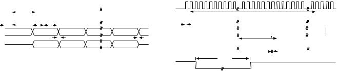
t1 |
|
|
|
|
|
|
|
|
|
|
|
|
|
||||||
SDFS |
|
|
|
|
t2 |
|
|
|
|
|
|
|
|
|
|
|
|
|
|
|
|
|
|
|
|
|
SDFS |
|
|
|
|
|
|
|
|
|
|
|
|
|
|
|
|
|
|
|
|
|
|
|
|
|
|
|
|
|
|||||||||
|
|
|
|
|
|
|
|
|
|
|
|
|
|
|
|
|
|
|
|
|
|
|
|
|
|
|
|
|
|
|
|
|
|
|
|
|
|
|
|
|
|
|
|
|
|
|
|
|
|
|
|
|
|
|
|
|
|
|
|
|
|||||
|
|
|
|
|
|
|
|
|
|
|
|
|
|
|
|
|
|
|
|
|
|
|
|
|
|
|
|
|
|
|
|
|
|
|
|
|
|
|
|
|
|
|
|
|
|
|
|
|
|
|
|
|
|
|
|
|
|
|
|
|
|
|
|
|
|
|
|
|
|
t |
|
|
|
t |
|
|
t |
|
|
|
|
|
|
|
|
|
|
|
|
|
|
|
|
|
|
tPD1 |
|
|
|
|
|
|
|
|
|
|
|
|
|
|
|
|
|
|
|
|
|
|
|
|
|
|
|
|
|||||||
|
|
|
|
PD1 |
|
|
|
S |
|
|
H |
|
|
|
|
|
|
|
|
|
|
|
|
|
|
|
|
|
|
|
|
|
|
|
|
|
|
|
|
|
|
|
|
|
|
|
|
|
|
|
|
|
|
|
|
|
|
|
|
|
|
|
|
|
|
SDI |
|
|
|
BIT 15 |
BIT 14 |
BIT 0 |
SDI OR SDO |
|
|
|
15 |
14 |
13 |
|
|
|
|
|
|
|
|
|
|
|
|
|
|
3 |
2 |
1 |
|
0 |
15 |
14 |
13 |
|
|
|
|
|
15 |
1413 |
|
||||||||||||||||||||||
|
|
|
|
|
|
|
|
|
|
|
|
|
|
|
|
tDV |
|
tHZ |
|
|
|
|
|
|
|
|
|
|
|
|
|
|
|
|
|
|
|
|
|
|
|
|
|
|
|
|
|
|
|
|
|
|
|
|
|
|
|||||||||
|
|
|
|
|
|
|
|
|
|
|
|
|
|
|
|
|
|
|
|
|
|
|
|
|
|
|
|
|
|
|
|
|
|
|
|
|
|
|
LAST |
|
|
|
|
|
|
|
|
|
|
|
|
|
|||||||||||||
|
|
|
|
|
|
|
|
|
|
|
|
|
|
|
|
|
|
|
|
|
|
|
|
|
|
|
|
|
|
|
|
|
|
|
|
|
|
|
|
|
|
|
|
|
|
VALID |
|
|
|
|
|
|
|
|
|
|
|
|
|
|
|||||
SDO |
|
|
|
BIT 15 |
BIT 14 |
BIT 0 |
TSO |
|
|
|
|
|
|
|
|
|
|
|
|
|
TIME SLOT |
|
|
|
|
|
|
|
|
|
|
|
|
|
|
||||||||||||||||||||||||||||||
|
|
|
|
|
|
|
|
|
|
|
|
|
|
|
|
|
|
|
|
|
|
|
|
|
|
|
|
|
|
|
|
|
|
|
|
|
|
|
|
|
|
|
|
|
|
|
|
|
|
|
|
|
|
|
|
|
|
|
|
|
|
|
|
|
|
tPD2
tRPWL
RESET
PWRDWN
Figure 1. Timing Diagrams
REV. 0 |
–5– |

AD1843
POWER SUPPLY (33 Ω HPOUT LOAD)
|
|
|
|
|
|
|
|
|
Min |
Typ |
Max |
Units |
Power Supply Range—Analog VCC |
4.75 |
|
5.25 |
V |
||||||||
Power Supply Range—Digital VDD |
2.85 |
|
5.25 |
V |
||||||||
Total Power Supply Current—5.0 VCC and VDD Operating |
|
|
|
|
||||||||
|
(5.0 VCC and VDD Supplies) |
|
210 |
250 |
mA |
|||||||
Total Power Supply Current—5.0 VCC/3.0 VDD Operating* |
|
|
|
|
||||||||
|
(5.0 VCC Analog/3.0 VDD Digital Supplies) |
|
150 |
175 |
mA |
|||||||
Analog Supply Current—5.0 VCC Operating |
|
60 |
75 |
mA |
||||||||
Digital Supply Current—5.0 VDD Operating |
|
150 |
175 |
mA |
||||||||
Digital Supply Current—3.0 VDD Operating* |
|
90 |
100 |
mA |
||||||||
Digital Power Supply Current—VDD Power Down ( |
PWRDWN |
LO) |
|
|
1 |
mA |
||||||
|
Analog Power Supply Current—VCC Power Down ( |
PWRDWN |
LO) |
|
|
0.5 |
mA |
|||||
Power Dissipation—5.0 VCC and VDD Operating (Current × Nominal Supply) |
|
|
1250 |
mW |
||||||||
|
Power Dissipation—5.0 VCC/3.0 VDD Operating* (Current × Nominal Supply) |
|
|
875 |
mW |
|||||||
Power Dissipation—5.0 VCC and VDD Power Down ( |
PWRDWN |
LO) |
|
|
|
|
||||||
|
(Current × Nominal Supply) |
|
|
7.5 |
mW |
|||||||
Power Dissipation—5.0 VCC/3.0 VDD Power Down* ( |
PWRDWN |
LO) |
|
|
|
|
||||||
|
(Current × Nominal Supply) |
|
|
5 |
mW |
|||||||
Power Supply Rejection (100 mV p-p Signal @ 1 kHz)* |
40 |
|
|
dB |
||||||||
|
(At Both Analog and Digital Supply Pins, for ADC, DAC1 and DAC2) |
|
|
|
|
|||||||
CLOCK SPECIFICATIONS* |
|
|
|
|
||||||||
|
|
|
|
|
|
|
|
|
|
|
|
|
|
|
|
|
|
|
|
|
|
Min |
Typ |
Max |
Units |
Input Crystal/Clock Frequency |
|
24.576 |
|
MHz |
||||||||
Input Clock Duty Cycle (When an External Clock Is Used Instead of a Crystal) |
25/75 |
|
75/25 |
% |
||||||||
Initialization Sample Rate Change Time |
|
|
0 |
ms |
||||||||
PACKAGE CHARACTERISTICS |
|
|
|
|
||||||||
|
|
|
|
|
|
|
|
|
|
|
|
|
|
|
|
|
|
|
|
|
|
|
Typ |
|
Units |
|
PQFP θJA (Thermal Resistance [Junction-to-Ambient]) |
|
96 |
|
°C/W |
|||||||
PQFP θJC (Thermal Resistance [Junction-to-Case]) |
|
8.75 |
|
°C/W |
||||||||
TQFP θJA (Thermal Resistance [Junction-to-Ambient]) |
|
30.6 |
|
°C/W |
||||||||
TQFP θJC (Thermal Resistance [Junction-to-Case]) |
|
4.6 |
|
°C/W |
||||||||
NOTES
1The stopband repeats itself at multiples of 64 × FS, where FS is the sampling frequency. Thus the audio mode digital filter will attenuate to –91.8 dB or better across |
|||||||||||||
|
the frequency spectrum except for a range of ± 0.6 × FS wide at multiples of 64 × FS. |
|
|
|
|
|
|
|
|||||
2The stopband repeats itself at multiples of 64 × FS, where FS is the sampling frequency. Thus the modem mode digital filter will attenuate to –75.7 dB or better across |
|||||||||||||
|
the frequency spectrum except for a range of ± 0.542 × FS wide at multiples of 64 × FS. |
|
|
|
|
|
|
||||||
3The stopband repeats itself at multiples of 64 × FS, where FS is the sampling frequency. Thus the resampler mode digital filter will attenuate to –92.2 dB or better |
|||||||||||||
|
across the frequency spectrum except for a range of ± 0.5 × FS wide at multiples of 64 × FS. |
|
|
|
|
|
|
||||||
*Guaranteed, not tested. |
|
|
|
|
|
|
|
|
|
|
|
||
Specifications subject to change without notice. |
|
|
|
|
|
|
|
|
|
|
|||
|
ABSOLUTE MAXIMUM RATINGS* |
|
|
|
*Stresses greater than those listed under “Absolute Maximum Ratings” may cause |
||||||||
|
|
|
|
|
|
|
permanent damage to the device. This is a stress rating only and functional |
||||||
|
|
|
Min |
Max |
Units |
||||||||
|
|
|
operation of the device at these or any other conditions above those indicated in the |
||||||||||
|
Power Supplies |
|
|
|
|
operational section of this specification is not implied. Exposure to absolute |
|||||||
|
Digital (VDD) |
–0.3 |
6.0 |
V |
maximum rating conditions for extended periods may affect device reliability. |
||||||||
|
|
|
|
|
|
|
|
||||||
|
Analog (VCC) |
–0.3 |
6.0 |
V |
|
ORDERING INFORMATION |
|
|
|||||
|
Input Current |
|
±10.0 |
|
|
|
|
|
|||||
|
|
|
|
|
|
|
|
|
|
|
|||
|
(Except Supply Pins) |
|
mA |
|
|
|
|
|
|
|
|||
|
|
|
Temperature |
Package |
Package |
||||||||
|
Analog Input Voltage (Signal Pins) |
–0.3 |
VCC + 0.3 |
V |
|
||||||||
|
Model |
Range |
Description |
Option |
|||||||||
|
Digital Input Voltage (Signal Pins) |
–0.3 |
VDD + 0.3 |
V |
|||||||||
|
|
|
|
|
|
|
|
||||||
|
Ambient Temperature (Operating) |
0 |
+70 |
°C |
AD1843JS |
0°C to +70°C |
80-Lead PQFP |
S-80 |
|||||
|
Storage Temperature |
–65 |
+150 |
°C |
|||||||||
|
AD1843JST |
0°C to +70°C |
100-Lead TQFP |
ST-100 |
|||||||||
|
ESD Tolerance (Human Body |
1000 |
|
V |
|||||||||
|
|
|
|
|
|
|
|
|
|||||
|
|
|
|
|
|
|
|
|
|||||
|
Model per Method 3015.2 |
|
|
|
|
|
|
|
|
|
|
|
|
|
of MIL-STD-883B) |
|
|
|
|
|
|
|
|
|
|
|
|
|
|
|
|
|
|
|
|
|
|
|
|
|
|
CAUTION |
|
|
|
|
|
|
|
|
|
|
|
|
|
ESD (electrostatic discharge) sensitive device. Electrostatic charges as high as 4000 V readily |
|
|
|
|
|||||||||
|
WARNING! |
|
|
||||||||||
accumulate on the human body and test equipment and can discharge without detection. |
|
|
|
||||||||||
Although the AD1843 features proprietary ESD protection circuitry, permanent damage may |
|
|
|
|
|||||||||
occur on devices subjected to high energy electrostatic discharges. Therefore, proper ESD |
|
ESD SENSITIVE DEVICE |
|
||||||||||
precautions are recommended to avoid performance degradation or loss of functionality. |
|
|
|||||||||||
|
|
|
|
||||||||||
|
|
|
|
|
|
|
|
|
|
|
|
|
|
–6– |
REV. 0 |

AD1843
PIN CONFIGURATIONS
80-Lead PQFP
|
|
|
SDI |
|
SCLK |
|
GNDD |
|
V |
|
CLKOUT |
|
CONV3 |
|
BIT3 |
|
GNDD |
|
V |
|
CONV2 |
|
BIT2 |
GNDD |
|
V |
|
CONV1 |
|
BIT1 |
|
GNDD |
|
V |
|
V |
|
XTALO |
|
XTALI |
|
|||
|
|
|
|
|
|
|
|
|
DD |
|
|
|
|
|
|
|
|
|
DD |
|
|
|
|
|
|
|
DD |
|
|
|
|
|
|
|
DD |
|
DD |
|
|
|
|
|
|
|
|
|
|
80 |
|
79 |
|
78 |
|
77 |
|
76 |
|
75 |
|
74 |
|
73 |
|
72 |
|
71 |
|
70 |
|
69 |
|
68 |
|
67 |
|
66 |
|
65 |
|
64 |
|
63 |
|
62 |
|
61 |
|
|
|
SDO |
|
|
|
|
|
|
|
|
|
|
|
|
|
|
|
|
|
|
|
|
|
|
|
|
|
|
|
|
|
|
|
|
|
|
|
|
|
|
|
|
|
|
|
GNDD |
|
|
|
|
|
|
|
|
|
|
|
|
|
|
|
|
|
|
|
|
|
|
|
|
|
|
|
|
|
|
|
|
|
|
|
|
|
|
|
|
|
||||
1 |
|
|
|
|
|
|
|
|
|
|
|
|
|
|
|
|
|
|
|
|
|
|
|
|
|
|
|
|
|
|
|
|
|
|
|
|
|
|
|
60 |
||||
SDFS |
|
|
|
|
|
|
|
|
|
|
|
|
|
|
|
|
|
|
|
|
|
|
|
|
|
|
|
|
|
|
|
|
|
|
|
|
|
|
|
|
|
|
|
|
2 |
|
|
|
|
|
|
|
|
|
|
|
|
|
|
|
|
|
|
|
|
|
|
|
|
|
|
|
|
|
|
|
|
|
|
|
|
|
|
|
59 |
XCTL1 |
|||
GNDD |
|
|
|
|
|
|
|
|
|
|
|
|
|
|
|
|
|
|
|
|
|
|
|
|
|
|
|
|
|
|
|
|
|
|
|
|
|
|
|
|
|
|
|
|
3 |
|
|
|
|
|
|
|
|
|
|
|
|
|
|
|
|
|
|
|
|
|
|
|
|
|
|
|
|
|
|
|
|
|
|
|
|
|
|
|
58 |
XCTL0 |
|||
VDD |
|
|
|
|
|
|
|
|
|
|
|
|
|
|
|
|
|
|
|
|
|
|
|
|
|
|
|
|
|
|
|
|
|
|
|
|
|
|
|
|
|
|
|
|
4 |
|
|
|
|
|
|
|
|
|
|
|
|
|
|
|
|
|
|
|
|
|
|
|
|
|
|
|
|
|
|
|
|
|
|
|
|
|
|
|
57 |
SYNC3 |
|||
TSI |
5 |
|
|
|
|
|
|
|
|
|
|
|
|
|
|
|
|
|
|
|
|
|
|
|
|
|
|
|
|
|
|
|
|
|
|
|
|
|
|
|
56 |
SYNC2 |
||
TSO |
|
|
|
|
|
|
|
|
|
|
|
|
|
|
|
|
|
|
|
|
|
|
|
|
|
|
|
|
|
|
|
|
|
|
|
|
|
|
|
|
|
|
|
|
6 |
|
|
|
|
|
|
|
|
|
|
|
|
|
|
|
|
|
|
|
|
|
|
|
|
|
|
|
|
|
|
|
|
|
|
|
|
|
|
|
55 |
SYNC1 |
|||
GNDD |
|
|
|
|
|
|
|
|
|
|
|
|
|
|
|
|
|
|
|
|
|
|
|
|
|
|
|
|
|
|
|
|
|
|
|
|
|
|
|
|
|
|
|
|
7 |
|
|
|
|
|
|
|
|
|
|
|
|
|
|
|
|
|
|
|
|
|
|
|
|
|
|
|
|
|
|
|
|
|
|
|
|
|
|
|
54 |
GNDD |
|||
VDD |
|
|
|
|
|
|
|
|
|
|
|
|
|
|
|
|
|
|
|
|
|
|
|
|
|
|
|
|
|
|
|
|
|
|
|
|
|
|
|
|
|
|
|
VDD |
8 |
|
|
|
|
|
|
|
|
|
|
|
|
|
|
|
|
|
|
|
|
|
|
|
|
|
|
|
|
|
|
|
|
|
|
|
|
|
|
|
53 |
||||
CS |
|
|
|
|
|
|
|
|
|
|
|
|
|
|
|
|
|
|
|
|
|
|
|
|
|
|
|
|
|
|
|
|
|
|
|
|
|
|
|
|
|
|
|
RESET |
9 |
|
|
|
|
|
|
|
|
|
|
|
|
|
|
|
|
|
|
|
|
|
|
|
|
|
|
|
|
|
|
|
|
|
|
|
|
|
|
|
52 |
||||
BM |
|
|
|
|
|
|
|
|
|
|
|
|
|
|
|
|
|
|
|
AD1843 |
|
|
|
|
|
|
|
|
|
|
|
|
|
|
|
|
|
|
|
PWRDWN |
||||
10 |
|
|
|
|
|
|
|
|
|
|
|
|
|
|
|
|
|
|
|
|
|
|
|
|
|
|
|
|
|
|
|
|
|
|
51 |
|||||||||
AUX3R |
|
|
|
|
|
|
|
|
|
|
|
|
|
|
|
|
|
|
|
TOP VIEW |
|
|
|
|
|
|
|
|
|
|
|
|
|
|
|
|
|
|
|
VDD |
||||
11 |
|
|
|
|
|
|
|
|
|
|
|
|
|
|
|
|
|
|
|
|
|
|
|
|
|
|
|
|
|
|
|
|
|
|
|
|
50 |
|||||||
|
|
|
|
|
|
|
|
|
|
|
|
|
|
|
|
|
(Not to Scale) |
|
|
|
|
|
|
|
|
|
|
|
|
|
|
|
||||||||||||
AUX3L |
|
|
|
|
|
|
|
|
|
|
|
|
|
|
|
|
|
|
|
|
|
|
|
|
|
|
|
|
|
|
|
|
|
|
|
|
|
|||||||
12 |
|
|
|
|
|
|
|
|
|
|
|
|
|
|
|
|
|
|
|
|
|
|
|
|
|
|
|
|
|
|
|
|
|
|
|
|
|
|
|
49 |
PDMNFT |
|||
AUX2R |
|
|
|
|
|
|
|
|
|
|
|
|
|
|
|
|
|
|
|
|
|
|
|
|
|
|
|
|
|
|
|
|
|
|
|
|
|
|
|
|
|
|
|
GNDA |
13 |
|
|
|
|
|
|
|
|
|
|
|
|
|
|
|
|
|
|
|
|
|
|
|
|
|
|
|
|
|
|
|
|
|
|
|
|
|
|
|
48 |
||||
AUX2L |
|
|
|
|
|
|
|
|
|
|
|
|
|
|
|
|
|
|
|
|
|
|
|
|
|
|
|
|
|
|
|
|
|
|
|
|
|
|
|
|
|
|
|
HPOUTL |
14 |
|
|
|
|
|
|
|
|
|
|
|
|
|
|
|
|
|
|
|
|
|
|
|
|
|
|
|
|
|
|
|
|
|
|
|
|
|
|
|
47 |
||||
AUX1R |
|
|
|
|
|
|
|
|
|
|
|
|
|
|
|
|
|
|
|
|
|
|
|
|
|
|
|
|
|
|
|
|
|
|
|
|
|
|
|
|
|
|
|
HPOUTC |
15 |
|
|
|
|
|
|
|
|
|
|
|
|
|
|
|
|
|
|
|
|
|
|
|
|
|
|
|
|
|
|
|
|
|
|
|
|
|
|
|
46 |
||||
AUX1L |
|
|
|
|
|
|
|
|
|
|
|
|
|
|
|
|
|
|
|
|
|
|
|
|
|
|
|
|
|
|
|
|
|
|
|
|
|
|
|
|
|
|
|
HPOUTR |
16 |
|
|
|
|
|
|
|
|
|
|
|
|
|
|
|
|
|
|
|
|
|
|
|
|
|
|
|
|
|
|
|
|
|
|
|
|
|
|
|
45 |
||||
MICR |
|
|
|
|
|
|
|
|
|
|
|
|
|
|
|
|
|
|
|
|
|
|
|
|
|
|
|
|
|
|
|
|
|
|
|
|
|
|
|
|
|
|
|
|
17 |
|
|
|
|
|
|
|
|
|
|
|
|
|
|
|
|
|
|
|
|
|
|
|
|
|
|
|
|
|
|
|
|
|
|
|
|
|
|
|
44 |
VCC |
|||
MICL |
18 |
|
|
|
|
|
|
|
|
|
|
|
|
|
|
|
|
|
|
|
|
|
|
|
|
|
|
|
|
|
|
|
|
|
|
|
|
|
|
|
43 |
SUML |
||
MIN |
|
|
|
|
|
|
|
|
|
|
|
|
|
|
|
|
|
|
|
|
|
|
|
|
|
|
|
|
|
|
|
|
|
|
|
|
|
|
|
|
|
|
|
SUMR |
19 |
|
|
|
|
|
|
|
|
|
|
|
|
|
|
|
|
|
|
|
|
|
|
|
|
|
|
|
|
|
|
|
|
|
|
|
|
|
|
|
42 |
||||
VCC |
|
|
|
|
|
|
|
|
|
|
|
|
|
|
|
|
|
|
|
|
|
|
|
|
|
|
|
|
|
|
|
|
|
|
|
|
|
|
|
|
|
|
|
|
20 |
|
|
|
|
|
|
|
|
|
|
|
|
|
|
|
|
|
|
|
|
|
|
|
|
|
|
|
|
|
|
|
|
|
|
|
|
|
|
|
41 |
VCC |
|||
|
|
|
|
|
|
|
|
|
|
|
|
|
|
|
|
|
|
|
|
|
|
|
|
|
|
|
|
|
|
|
|
|
|
|
|
|
|
|
|
|
|
|
|
|
|
|
21 |
|
22 |
|
23 |
|
24 |
|
25 |
|
26 |
|
27 |
|
28 |
|
29 |
|
30 |
|
31 |
|
32 |
|
33 |
|
34 |
|
35 |
|
36 |
|
37 |
|
38 |
|
39 |
|
40 |
|
|
|
|
|
|
|
|
|
|
|
|
|
|
|
|
|
|
|
|
|
|
|
|
|
|
|
|
|
|
|
|
|
|
|
|
|
|
|
|
|
|
|
|
|
|
|
|
|
|
|
|
GNDA |
|
AAFILTR |
|
FILTR |
|
AAFILTL |
|
FILTL |
|
LINRP |
|
LINRN |
|
LINLP |
|
LINLN |
|
LOUT2RP |
|
LOUT2RN |
LOUT2LP |
|
LOUT2LN |
|
LOUT1R |
|
MOUT |
|
LOUT1L |
|
GNDA |
|
CMOUT |
|
V |
|
GNDA |
|
|||
|
|
|
|
|
|
|
|
|
|
|
|
|
|
|
|
|
|
|
|
|
|
|
|
|
|
|
|
|
|
|
|
|
|
|
|
|
|
|
REF |
|
|
|
|
|
PIN DESCRIPTION
Serial Interface
Pin Name |
PQFP |
TQFP |
I/O |
Description |
||
|
|
|
|
|
|
|
SCLK |
79 |
99 |
I/O |
Serial Clock. SCLK is a bidirectional signal that supplies the clock as an output |
||
|
|
|
|
to the serial bus when the Bus Master (BM) pin is driven HI and accepts the clock |
||
|
|
|
|
as an input when the BM pin is driven LO. When the AD1843 is configured in |
||
|
|
|
|
master mode, the SCLK frequency may be set to either 12.288 MHz or 16.384 MHz |
||
|
|
|
|
with the SCF bit in Control Register Address 26. |
||
SDFS |
2 |
2 |
I/O |
Serial Data Frame Sync. SDFS is a bidirectional signal that supplies the frame |
||
|
|
|
|
synchronization signal as an output to the serial bus when the Bus Master (BM) |
||
|
|
|
|
pin is driven HI and accepts the frame synchronization signal as an input when |
||
|
|
|
|
the BM pin is driven LO. |
||
SDI |
80 |
100 |
I |
Serial Data Input. SDI is used by peripheral devices such as the host CPU or a |
||
|
|
|
|
DSP to supply control and playback data information to the AD1843. All control |
||
|
|
|
|
and playback transfers are 16 bits long, MSB first. |
||
SDO |
1 |
1 |
O |
Serial Data Output. SDO is used to supply status/control register readback and |
||
|
|
|
|
capture data information to peripheral devices such as the host CPU or a DSP. |
||
|
|
|
|
All status/control register readback and capture data transfers are 16 bits long, |
||
|
|
|
|
MSB first. A three-state output driver is used on this pin. |
||
BM |
10 |
12 |
I |
Bus Master. When BM is tied HI the AD1843 is the serial bus master. The |
||
|
|
|
|
AD1843 will then supply the serial clock (SCLK) and the frame sync (SDFS) |
||
|
|
|
|
signals for the serial bus. No more than one device (AD1843/CPU/DSP) should |
||
|
|
|
|
be configured as the serial bus master. When BM is tied LO, the AD1843 is con- |
||
|
|
|
|
figured as a bus slave, and will accept the SCLK and SDFS signals as inputs. The |
||
|
|
|
|
logic level on this pin must not be changed once |
RESET |
is deasserted (driven HI). |
|
|
|
|
|
|
|
REV. 0 |
–7– |
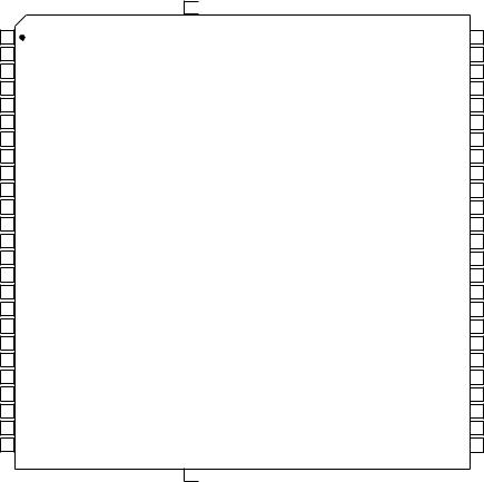
AD1843
PIN CONFIGURATIONS
100-Lead TQFP
SDI |
|
SCLK |
|
NC |
|
GNDD |
|
V |
|
CLKOUT |
|
CONV3 |
|
NC |
|
BIT3 |
|
|
|
|
|
|
|
|
DD |
|
|
|
|
|
|
|
|
100 |
|
99 |
|
98 |
|
97 |
|
96 |
|
95 |
|
94 |
|
93 |
|
92 |
|
|
|
|
|
|
|
|
|
|
|
|
|
|
|
|
|
SDO 1
SDFS 2
NC 3
GNDD 4
VDD 5
TSI 6
TSO 7
NC 8
GNDD 9
VDD 10
CS 11
BM 12
NC 13
NC 14
AUX3R 15
AUX3L 16
AUX2R 17
AUX2L 18
AUX1R 19
AUX1L 20
MICL 21
MICR 22
MIN 23
NC 24
VCC 25
26 |
|
27 |
|
28 |
|
29 |
|
30 |
|
31 |
|
32 |
|
33 |
|
34 |
|
|
|
|
|
|
|
|
|
|
|
|
|
|
|
|
|
NC |
|
GNDA |
|
AAFILTR |
|
FILTR |
|
AAFILTL |
|
FILTL |
|
NC |
|
LINRP |
|
LINRN |
NC = NO CONNECT
GNDD |
|
V |
|
CONV2 |
|
NC |
|
BIT2 |
|
GNDD |
|
V |
|
CONV1 |
|
NC |
|
BIT1 |
|
GNDD |
|
V |
|
V |
|
NC |
|
XTALO |
|
XTALI |
|
|
DD |
|
|
|
|
|
|
|
|
|
DD |
|
|
|
|
|
|
|
|
|
DD |
|
DD |
|
|
|
|
|
|
91 |
|
90 |
|
89 |
|
88 |
|
87 |
|
86 |
|
85 |
|
84 |
|
83 |
|
82 |
|
81 |
|
80 |
|
79 |
|
78 |
|
77 |
|
76 |
|
|
|
|
|
|
|
|
|
|
|
|
|
|
|
|
|
|
|
|
|
|
|
|
|
|
|
|
|
|
|
AD1843
TOP VIEW (Not to Scale)
35 |
|
36 |
|
37 |
|
38 |
|
39 |
|
40 |
|
41 |
|
42 |
|
43 |
|
44 |
|
45 |
|
46 |
|
47 |
|
48 |
|
49 |
|
50 |
LINLP |
|
|
|
|
|
|
|
|
|
|
|
|
|
|
|
|
|
|
|
|
|
|
|
|
|
|
|
|
|
|
|
LINLN |
|
NC |
|
LOUT2RP |
|
LOUT2RN |
|
LOUT2LP |
|
LOUT2LN |
|
NC |
|
LOUT1R |
|
MOUT |
|
LOUT1L |
|
GNDA |
|
CMOUT |
|
V |
|
GNDA |
|
NC |
|
|
|
|
|
|
|
|
|
|
|
|
|
|
|
|
|
|
|
|
|
|
|
|
|
|
|
REF |
|
|
|
|
75 GNDD
74 XCTL1
73 NC
72 XCTL0
71 SYNC3
70 SYNC2
69 SYNC1
68 NC
67 GNDD
66 VDD
65 RESET
64 PWRDWN
63 NC
62 VDD
61 PDMNFT
60 NC
59 GNDA
58 HPOUTL
57 HPOUTC
56 HPOUTR
55 VCC
54 SUML
53 SUMR
52 NC
51 VCC
Serial Interface (Continued)
Pin Name |
PQFP |
TQFP |
I/O |
Description |
||
|
|
|
|
|
|
|
CS |
9 |
11 |
I |
Chip Select. When CS is set HI, the serial interface I/O pins will be in their normal |
||
|
|
|
|
active states. When CS is reset LO, SCLK, SDFS, and SDO are three- |
||
|
|
|
|
stated; SCLK, SDFS and SDI inputs are ignored; and TSO drives out the logic |
||
|
|
|
|
level received on TSI. |
||
TSO |
6 |
7 |
O |
Time Slot Output. TSO is asserted HI by the AD1843 simultaneously with the LSB |
||
|
|
|
|
of the last time slot used by the AD1843. It is used to daisy-chain multiple AD1843s |
||
|
|
|
|
on a common TDM serial bus. If the power-down ( |
PWRDWN |
) pin is asserted or if |
|
|
|
|
the chip select pin (CS) is deasserted, TSO is set to the logic level on the TSI pin, |
||
|
|
|
|
allowing powered-down or unselected AD1843s on a daisy-chain to be skipped. |
||
TSI |
5 |
6 |
I |
Time Slot Input. Asserting TSI HI indicates to the AD1843 that it should use |
||
|
|
|
|
the next six time slots beginning on the next SCLK period. It also enables TSO |
||
|
|
|
|
to be asserted at the end of these six time slots. TSI is ignored (but should be tied |
||
|
|
|
|
LO) when the AD1843 is the bus master since the bus master uses the first time |
||
|
|
|
|
slots in a TDM frame. |
||
XCTL[1:0] |
59, 58 |
72, 74 |
I/O |
External Control. These signals reflect the status of bits (Data 8 and 9) in Control |
||
|
|
|
|
Register Address 28 of the AD1843. They may be used for signaling or controlling |
||
|
|
|
|
external logic. |
||
|
|
|
|
|
|
|
–8– |
REV. 0 |

AD1843
Analog Signals
Pin Name |
PQFP |
TQFP |
I/O |
Description |
|
|
|
|
|
LINLP |
28 |
35 |
I |
Line Input Left Channel Positive Differential Signal. |
LINLN |
29 |
36 |
I |
Line Input Left Channel Negative Differential Signal. |
LINRP |
26 |
33 |
I |
Line Input Right Channel Positive Differential Signal. |
LINRN |
27 |
34 |
I |
Line Input Right Channel Negative Differential Signal. |
MICL |
18 |
21 |
I |
Microphone Input Left Channel. Microphone input for the left channel. This |
|
|
|
|
signal can be either line level or –20 dB from line level. |
MICR |
17 |
22 |
I |
Microphone Input Right Channel. Microphone input for the right channel. |
|
|
|
|
This signal can be either line level or –20 dB from line level. |
AUX1L |
16 |
20 |
I |
Auxiliary #1 Left Channel Line Input. |
AUX1R |
15 |
19 |
I |
Auxiliary #1 Right Channel Line Input. |
AUX2L |
14 |
18 |
I |
Auxiliary #2 Left Channel Line Input. |
AUX2R |
13 |
17 |
I |
Auxiliary #2 Right Channel Line Input. |
AUX3L |
12 |
16 |
I |
Auxiliary #3 Left Channel Line Input. |
AUX3R |
11 |
15 |
I |
Auxiliary #3 Right Channel Line Input. |
MIN |
19 |
23 |
I |
Monaural (Mono) Line Input. |
MOUT |
35 |
44 |
O |
Monaural (Mono) Line Output. |
LOUT1L |
36 |
45 |
O |
Line Output #1 Left Channel. |
LOUT1R |
34 |
43 |
O |
Line Output #1 Right Channel. |
HPOUTL |
47 |
58 |
O |
Headphone Output Left Channel. |
HPOUTC |
46 |
57 |
|
Headphone Common Return. |
HPOUTR |
45 |
56 |
O |
Headphone Output Right Channel. |
LOUT2LP |
32 |
40 |
O |
Line Output #2 Left Channel Positive Differential Signal. |
LOUT2LN |
33 |
41 |
O |
Line Output #2 Left Channel Negative Differential Signal. |
LOUT2RP |
30 |
38 |
O |
Line Output #2 Right Channel Positive Differential Signal. |
LOUT2RN |
31 |
39 |
O |
Line Output #2 Right Channel Negative Differential Signal. |
SUML |
43 |
54 |
I |
Mixer Line Input Left Channel. |
SUMR |
42 |
53 |
I |
Mixer Line Input Right Channel. |
|
|
|
|
|
Clocks |
|
|
|
|
Pin Name |
PQFP |
TQFP |
I/O |
Description |
|
|
|
|
|
CLKOUT |
76 |
95 |
O |
Clock Output. This signal is a buffered version of XTALO (with a duty cycle |
|
|
|
|
restored to at least 60%/40%), the crystal clock output. This pin is enabled by |
|
|
|
|
default but can be three-stated by programming a bit in Control Register |
|
|
|
|
Address 28. The CLKOUT frequency is 24.576 MHz. |
SYNC[3:1] |
57, 56, 55 |
71, 70, 69 |
I |
Sync Inputs. These SYNC signals are used as the clock source inputs to three |
|
|
|
|
receptive PLLs in the AD1843. These pins accept a clock at, or at a multiple of, |
|
|
|
|
the desired sample rate for A-to-D and D-to-A conversions. These inputs are |
|
|
|
|
ignored if a sample rate is programmed directly, but should never be left floating. |
CONV[3:1] |
75, 71, 67 |
94, 89, 84 |
O |
Conversion Clock Outputs. These output clocks have an average period equal to (or 128 |
|
|
|
|
times) the internal sample rates of the AD1843. These clock outputs are three-stated |
|
|
|
|
by default but can be enabled by programming bits in Control Register Address 28. |
BIT[3:1] |
74, 70, 66 |
92, 87, 82 |
O |
Bit Clock Outputs. These output clocks can be individually programmed to |
|
|
|
|
multiples of the sample rates. Support for V.34 or V.32 bit rates is available. |
|
|
|
|
These clock outputs are three-stated by default but can be enabled by |
|
|
|
|
programming bits in Control Register Address 28. |
|
|
|
|
|
REV. 0 |
–9– |
AD1843
Miscellaneous
|
|
|
|
|
|
|
|
|
|
|
|
|
|
|
|
|
|
|
|
|
|
|
|
Pin Name |
|
PQFP |
TQFP |
I/O |
Description |
||||||||||||||||||
|
|
|
|
|
|
|
|
|
|
|
|
|
|
|
|
|
|
|
|
|
|
|
|
XTALI |
|
61 |
76 |
I |
24.576 MHz Crystal Input. When using a crystal as the clock source, the crystal |
||||||||||||||||||
|
|
|
|
|
|
|
|
should be connected between the XTALI and XTALO pins. This crystal should |
|||||||||||||||
|
|
|
|
|
|
|
|
be 24.576 MHz for the normal sampling rate range, i.e., 4 kHz to 54 kHz. A |
|||||||||||||||
|
|
|
|
|
|
|
|
clock input (perhaps the CLKOUT of another AD1843) may be driven into |
|||||||||||||||
|
|
|
|
|
|
|
|
XTALI in place of a crystal. The external clock input must be greater than or equal |
|||||||||||||||
|
|
|
|
|
|
|
|
to 512 times the maximum desired AD1843 sampling frequency. |
|||||||||||||||
XTALO |
|
62 |
77 |
O |
24.576 MHz Crystal Output. When using a crystal as the clock source, the crystal |
||||||||||||||||||
|
|
|
|
|
|
|
|
should be connected between the XTALI and XTALO pins. If a clock is driven |
|||||||||||||||
|
|
|
|
|
|
|
|
directly into XTALI, then XTALO should be left unconnected. |
|||||||||||||||
|
|
|
|
51 |
64 |
I |
|
Power Down. |
|
|
|
|
is active LO. The assertion of this signal will initialize |
||||||||||
PWRDWN |
PWRDWN |
||||||||||||||||||||||
|
|
|
|
|
|
|
|
the on-chip Control Registers to their default values, and will completely and |
|||||||||||||||
|
|
|
|
|
|
|
|
quietly power down the AD1843. If a crystal is not connected between XTALI |
|||||||||||||||
|
|
|
|
|
|
|
|
and XTALO, there must be a 24.576 MHz clock input on XTALI for at least |
|||||||||||||||
|
|
|
|
|
|
|
|
5 ms after this signal is asserted LO for proper operation. The AD1843 will not |
|||||||||||||||
|
|
|
|
|
|
|
|
be completely powered down until after this 5 ms period elapses. The AD1843 |
|||||||||||||||
|
|
|
|
|
|
|
|
always finishes an in-progress power-up sequence before initiating a power-down |
|||||||||||||||
|
|
|
|
|
|
|
|
sequence, and vice versa. If the |
PWRDWN |
pin is asserted while a power-up sequence |
|||||||||||||
|
|
|
|
|
|
|
|
is in progress, the 24.576 MHz clock signal on XTALI must persist for a worst |
|||||||||||||||
|
|
|
|
|
|
|
|
case maximum of 479 ms (power up = 470 ms, autocalibration = 4 ms, power |
|||||||||||||||
|
|
|
|
|
|
|
|
down = 5 ms) after |
PWRDWN |
is asserted. When INIT (Control Register |
|||||||||||||
|
|
|
|
|
|
|
Address 0, Bit 15) is set to a “1,” the power-down sequence is complete. See |
||||||||||||||||
|
|
|
|
|
|
|
the “Power Management” section for important additional details. |
||||||||||||||||
|
|
|
|
52 |
65 |
I |
|
Reset. |
|
|
is active LO. The assertion of this signal will initialize the on-chip |
||||||||||||
RESET |
RESET |
||||||||||||||||||||||
|
|
|
|
|
|
|
registers to their default values, and will completely power down the AD1843. |
||||||||||||||||
|
|
|
|
|
|
|
|
RESET |
is similar to |
PWRDWN |
, except that when |
PWRDWN |
is asserted, power |
||||||||||
|
|
|
|
|
|
|
down is “quiet” and performed synchronously to the internal clocks. When |
RESET |
|
||||||||||||||
|
|
|
|
|
|
|
is asserted, power down is “noisy” and performed asynchronously to the internal |
||||||||||||||||
|
|
|
|
|
|
|
clocks. |
||||||||||||||||
PDMNFT |
|
49 |
61 |
I |
Power-Down Mono Feedthrough. When the AD1843 mixer is powered down, |
||||||||||||||||||
|
|
|
|
|
|
|
and PDMNFT is asserted HI, the Mono Input (MIN, PQFP Pin 19) is routed to |
||||||||||||||||
|
|
|
|
|
|
|
the Mono Output (MOUT, PQFP Pin 35), and the signal applied to MIN will |
||||||||||||||||
|
|
|
|
|
|
|
feedthrough to MOUT. When the AD1843 mixer is powered down and |
||||||||||||||||
|
|
|
|
|
|
|
PDMNFT is deasserted LO, the feedthrough of MIN to MOUT will be muted. |
||||||||||||||||
|
|
|
|
|
|
|
When the AD1843 mixer is not powered down, and MIN to MOUT feedthrough |
||||||||||||||||
|
|
|
|
|
|
|
is desired, the Mono Input Mix Mute (Control Register Address 8, Bit 15) and the |
||||||||||||||||
|
|
|
|
|
|
|
Mono Output Mute (Control Register Address 8, Bit 6) must be unmuted. During |
||||||||||||||||
|
|
|
|
|
|
|
power-down feedthrough, the signal applied to the MIN input appears only at |
||||||||||||||||
|
|
|
|
|
|
|
the MOUT output. During normal operation, the signal applied to the MIN |
||||||||||||||||
|
|
|
|
|
|
|
input appears at both the MOUT and the LOUT1 outputs. The state of the |
||||||||||||||||
|
|
|
|
|
|
|
PDMNFT pin should be changed when the AD1843 mixer is powered up. If the |
||||||||||||||||
|
|
|
|
|
|
|
state of PDMNFT is changed when the AD1843 is in total power-down, audible |
||||||||||||||||
|
|
|
|
|
|
|
pops and clicks will likely result. |
||||||||||||||||
CMOUT |
|
38 |
47 |
O |
Common-Mode Voltage Output. Nominal 2.25 volt reference available externally |
||||||||||||||||||
|
|
|
|
|
|
|
for dc-coupling and level-shifting. CMOUT should not be used where it will sink |
||||||||||||||||
|
|
|
|
|
|
|
or source current. |
||||||||||||||||
VREF |
|
39 |
48 |
I |
|
Voltage Reference Filter. Voltage reference filter point for external bypassing only. |
|||||||||||||||||
FILTL |
|
25 |
31 |
I |
Left Channel Filter. This pin requires a 1.0 μF capacitor to analog ground for |
||||||||||||||||||
|
|
|
|
|
|
|
proper operation. |
||||||||||||||||
FILTR |
|
23 |
29 |
I |
Right Channel Filter. This pin requires a 1.0 μF capacitor to analog ground for |
||||||||||||||||||
|
|
|
|
|
|
|
proper operation. |
||||||||||||||||
AAFILTL |
|
24 |
30 |
I |
Left Channel Antialias Filter. This pin requires a 1000 pF capacitor to analog |
||||||||||||||||||
|
|
|
|
|
|
|
ground for proper operation. |
||||||||||||||||
AAFILTR |
|
22 |
28 |
I |
Right Channel Antialias Filter. This pin requires a 1000 pF capacitor to analog |
||||||||||||||||||
|
|
|
|
|
|
|
|
ground for proper operation. |
|||||||||||||||
|
|
|
|
|
|
|
|
|
|
|
|
|
|
|
|
|
|
|
|
|
|
|
|
–10– |
REV. 0 |
AD1843
POWER SUPPLIES
Pin Name |
PQFP |
TQFP |
I/O |
Description |
|
|
|
|
|
VCC |
20, 41, 44 |
25, 51, 55 |
I |
Analog Supply Voltage (+5 V). |
GNDA |
21, 37, 40, 48 |
27, 46, 49, 59 |
O |
Analog Ground. |
VDD |
4, 8, 50, 53, |
5, 10, 62, 66, |
I |
Digital Supply Voltage (+5/3 V). |
|
63, 64, 68, 72, |
79, 80, 85, 90, |
|
|
|
77 |
96 |
|
|
GNDD |
3, 7, 54, 60, |
4, 9, 67, 75, |
I |
Digital Ground. |
|
65, 69, 73, 78 |
81, 86, 91, 97 |
|
|
NC |
|
3, 8, 13, 14, |
|
No Connect. May be left floating. |
|
|
24, 26, 32, 37, |
|
|
|
|
42, 50, 52, 60, |
|
|
|
|
63, 68, 73, 78, |
|
|
|
|
83, 88, 93, 98 |
|
|
|
|
|
|
|
(continued from page 1)
The versatility of the device is shown by the following examples of functions it can perform:
•Stereo audio input and/or quad output, simultaneously at different sample rates
•Stereo audio output with simultaneous full duplex modem or fax operation with frequency and phase resampling
•Mono audio input and stereo audio output with simultaneous modem receive and transmit for simultaneous voice and data communications
•Dual independent audio inputs with audio output for echocancelling speakerphones
Audio Functional Description
The AD1843 SoundComm codec provides a complete audio solution with very few external components required. Dynamic range of the device exceeds 80 dB over the 20 kHz audio band and sample rates from 4 kHz to 49 kHz are supported (up to 54 kHz for a single channel if other channels are powered down). The audio functionality of this device is a superset of that found in the Analog Devices AD1848 SoundPort® device which has set the business audio standard throughout the computer industry.
Inputs to the device include a stereo microphone pair, a stereo line pair, a stereo CD input pair (AUX1), a stereo synthesized music input pair (AUX2), a dual phone line input (AUX3), a mono input, and a stereo input from an FM synthesizer (SUM). All of these inputs (except SUM) are multiplexed to the two åD A/D converters and are mixable directly as analog signals with the outputs of the D/A converters. All analog input signals (except SUM) can be amplified, attenuated or muted before mixing with the outputs of the D/A converters.
The device has two pairs of åD DACs which accept 8- or 16-bit digital data from the serial port. Each DAC pair’s independent sampling rate can either be programmed by Control Register (with 1 Hz resolution) or synchronized to an external input. The second pair of DACs can be used to replace the music synthesis DAC pair found on many audio products for PCs. Outputs from the AD1843 include a line output, a mono output, a stereo headphone output with its own current return path, and a
SoundPort is a registered trademark of Analog Devices, Inc.
differential stereo output for connection to a DAA. The line and differential outputs are looped back to the ADC input selector.
The AD1843’s mixing and routing capabilities are extensive. The digital data from both DAC channels after interpolation can be routed back to the ADC decimators, to support digital- to-digital sample rate conversion (digital resampling). Digital data from the ADC can also be routed to the two stereo DAC pairs, for a digital loopback mode which is helpful for devicelevel and board-level test. Digital data from either stereo DAC can be mixed with the digital data feeding the other DAC, and the analog signal from DAC2 can be mixed with the analog output from DAC1.
Sample rates are independently programmable in the range of 4 kHz to 54 kHz to a 1 Hz resolution or sample rates can be
synchronized to an external source. Up to three different signals can be applied to the device’s three digital phase lock loop SYNC inputs for external synchronization.
These SYNC inputs can also be used in a special mode for audio/video synchronization. In this mode, an NTSC or PAL derived clock signal (approximately 15 kHz) is applied to the SYNC inputs and the device produces one of a variety of standard audio sample rates (32 kHz, 44.056 kHz, 44.1 kHz and 48 kHz, and most of these divided by the integers 1 through 8). In this manner, video and audio sample rates which are mathematically unrelated can be locked together.
Data Communications/Telephony Functional Description
The AD1843 includes all data conversion, filtering, and clock generation circuitry needed to implement an echo-cancelling modem with a companion digital signal processor. Softwareprogrammable sample rates and clocking modes support all established modem standards including those for the V.34 standard.
The AD1843 utilizes advanced åD technology to move the entire echo-cancelling modem implementation into the digital domain. The device maintains 90 dB typical dynamic range throughout all filtering and data conversion across a 9.6 kHz passband. Purely DSP-based echo cancellation algorithms can maintain robust bit error rates under worst-case signal attenuation and echo amplitude conditions. The AD1843’s on-chip interpolation filter resamples (both frequency and phase) the received signal after echo cancellation in the DSP, freeing the processor for other voice or data communications tasks.
REV. 0 |
–11– |

|
|
LINLP |
|
|
LINLN |
|
|
LINRP |
|
|
LINRN |
|
|
MICL |
|
|
MICR |
|
|
AUX1L |
|
Figure |
AUX1R |
|
AUX2L |
|
|
|
|
|
|
AUX2R |
|
.2 |
AUX3L |
|
AUX3R |
|
|
Detailed |
|
|
MIN |
|
|
|
|
–12– |
Functional |
MUTE |
|
|
|
|
|
MOUT |
|
Block |
MUTE |
|
LOUT1L |
|
|
|
|
|
Diagram |
LOUT1R |
|
MUTE |
|
|
|
DRIVER |
|
|
HPOUTL |
|
|
HPOUTC |
|
|
HPOUTR |
|
|
LOUT2LP |
|
|
LOUT2LN |
|
|
LOUT2RP |
|
|
LOUT2RN |
|
|
SUML |
|
|
SUMR |
.REV
AD1843
XTALI XTALO SYNC3 SYNC2 SYNC1 CONV3 CONV2 CONV1 BIT3 |
BIT2 BIT1 |
CLOCK GENERATION |
CLKOUT |
|
20 dB |
|
|
|
|
S |
|
|
|
|
|
AD1843 |
|
|
|
|
|
|
|
E |
|
|
|
|
|
|
|
|
|
|
|
|
|
L |
|
|
|
|
|
|
|
|
|
|
|
|
|
E |
|
|
|
|
|
|
|
|
|
|
|
|
|
C |
|
|
|
|
|
|
|
|
|
|
|
|
|
T |
|
å D |
|
|
|
|
|
|
|
|
|
|
|
O |
PGA |
S |
|
|
|
|
|
|
|
|
|
|
|
R |
ADC |
|
|
|
|
||
|
|
|
|
|
|
E |
|
|
|
|
|||
|
|
|
|
|
|
|
LEFT |
|
|
|
|||
|
|
|
|
|
|
|
|
|
L |
|
|
|
|
|
|
|
|
|
|
|
|
S |
E |
RIGHT |
|
|
|
|
|
|
|
|
|
|
|
C |
|
|
|
||
|
|
|
|
|
|
|
|
E |
T |
|
|
|
|
|
|
|
|
|
|
|
|
L |
|
|
|
|
|
|
|
|
|
|
|
|
|
O |
|
|
|
|
|
|
|
|
|
|
|
|
|
E |
|
|
|
|
|
|
|
|
|
|
|
|
|
R |
|
|
|
|
|
|
|
|
|
|
|
|
|
C |
|
|
|
|
|
|
|
|
|
|
|
|
|
|
|
|
|
|
|
|
|
|
|
|
|
|
|
T |
|
|
|
|
|
|
|
|
|
|
|
|
|
O |
|
|
|
|
|
GN/AT |
GN/AT |
GN/AT |
GN/AT |
GN/AT |
|
|
|
R |
|
|
|
ATTN |
|
|
|
|
|
|
|
|
|
|
|
|
|
|
|
MUTE |
MUTE |
MUTE |
MUTE |
MUTE |
|
|
|
|
|
|
|
MUTE |
|
|
|
|
|
|
|
|
|
|
|
|
|
|
|
å |
å |
å |
å |
å |
MUTE |
GN/AT |
DACåD |
|
å |
MUTE |
|
å |
LEFT |
|
ATTN |
|
|||||||||||
å |
å |
å |
å |
å |
|
å |
å |
RIGHT |
|||||
|
|
|
|
|
|
||||||||
|
|
|
|
|
|
|
MUTE |
|
MUTE |
|
GN/AT = GAIN/ |
|
|
ATTENUATION |
GN/AT |
|
|
|
|
|
|
MUTE |
|
|
GN/AT |
|
|
||
|
|
|
|
LEFT
RIGHT
MUTE  ATTN
ATTN

 DAC åD
MUTE
å 

å
|
|
MUTE |
MUTE |
ATTN |
å |
å |
CONTROL REGISTERS
µ/A LAW
FIFO |
µ/A LAW |
FIFO |
µ/A LAW |
ADC
|
SCLK |
|
D |
SDFS |
|
|
||
I |
SDI |
|
G |
||
|
||
I |
SDO |
|
T |
||
A |
|
|
L |
BM |
|
DAC1 |
CS |
|
|
||
|
TSO |
|
I |
TSI |
|
N |
||
T |
2 |
E XCTL [1:0]
FPDMNFT
C
E RESET

 PWRDWN
DAC2
VOLTAGE REFERENCE
|
|
|
|
|
4 |
3 |
8 |
9 |
AAFILTL AAFILTR |
VREF |
CMOUT |
FILTL |
FILTR |
GNDA |
VCC |
GNDD |
VDD |
0
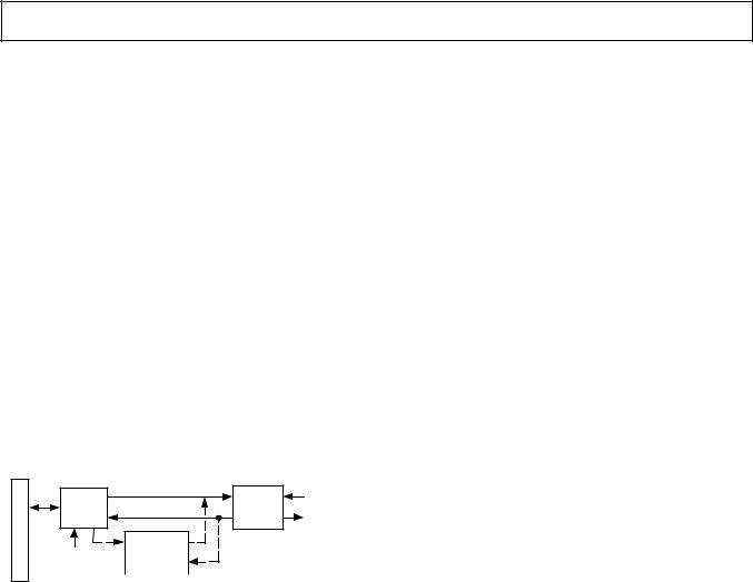
AD1843
On-chip bit and baud clock generation circuitry allows either synchronous or asynchronous operation of the transmit (DAC) and receive (ADC) paths. Each path features independent phase advance and retard adjustments via software control. The AD1843 can also synchronize modem operation to an external terminal band clock. Because the device has multiple input and output channels and converters, it is well suited for telephony applications requiring multiple channels for voice and modem.
A detailed block diagram of the AD1843 is shown in Figure 2.
DETAILED PRODUCT DESCRIPTION
The Serial-Port AD1843 SoundComm Codec integrates the key audio and PSTN data conversion and control functions into a single integrated circuit. The AD1843 is intended to provide a complete, single-chip audio and fax/modem solution for PC multimedia applications.
External circuit requirements are limited to a minimal number of low cost support components. Dynamic range exceeds 80 dB over the 20 kHz audio band. Sample rates from 4 kHz to
54 kHz with 1 Hz resolution are supported from a single external crystal or clock source.
The AD1843 SoundComm Codec is intended to be interfaced through a DSP chip or an ASIC to a host bus such as ISA, EISA or PCI. A general system architecture is shown in Figure 3.
S |
|
|
|
Y |
|
AD1843 |
|
S |
ASIC |
ANALOG I/O |
|
T |
|
|
|
E |
|
|
|
M |
|
|
|
B |
|
|
ADSP-21xx |
||||||||||
|
|||||||||||||
U |
|
|
|
|
|
|
|
|
|
|
|
|
|
|
|
|
|
|
|
|
|
|
|||||
S |
|
|
|
|
|||||||||
|
|
|
|
||||||||||
Figure 3. AD1843 System Diagram
The SoundComm codec includes a stereo pair of åD analog-to- digital converters and two stereo pairs of åD digital-to-analog converters. Inputs to the ADC can be selected from eight sources of analog signals: stereo line (LIN), stereo microphone (MIC), stereo auxiliary line #1 (AUX1), stereo auxiliary line #2 (AUX2), stereo auxiliary line #3 (AUX3), mono line (MIN), mixer output, and DAC2 output. A mono output and a stereo headphone driver are included on-chip. A stereo line level input (SUM) can be mixed into the output summer. A software-con- trolled programmable gain stage allows independent gain for each ADC channel. The ADCs’ output can be digitally mixed with both the DAC1 and DAC2 inputs. The left and right ADC channels can be configured for different sample rates and digital filter function (audio, modem or resampling).
The pair of 16-bit outputs from the ADCs is available over a serial interface that also supports 16-bit digital input to the DACs and control/status information. The AD1843 can accept and generate 16-bit twos-complement PCM linear digital data, 8-bit unsigned magnitude PCM linear data, and 8-bit m-law or A-law companded digital data. The data format is defined independently for each conversion resource on the AD1843.
The åD DACs are preceded by a four sample deep FIFO buffer and a digital interpolation filter. The DAC1 and DAC2 outputs can be mixed in the digital domain. Digital and analog attenuators provide independent user volume control (plus mute) over each DAC channel. Nyquist images and shaped quantized
noise are removed from the DACs’ analog stereo output by onchip switched-capacitor and continuous-time filters. All of the analog inputs (except the stereo line input) can be mixed with the DAC1 output in the analog domain. The DAC2 output can also be mixed with the DAC1 output in the analog domain. The DAC1 and DAC2 digital data can be fed back to the digital half of the ADC to enable digital resampling operation. DAC1 and DAC2 can be run at different sample rates and with different digital filter functions, without any beat frequency problems.
FUNCTIONAL DESCRIPTION
This section overviews the functionality of the AD1843 and is intended as a general introduction to the capabilities of the device. As much as possible, detailed reference information has been placed in “Control Registers” and other sections. The user is not expected to refer repeatedly to this section.
Analog Inputs
The AD1843 SoundComm Codec accepts stereo line-level and mic-level inputs. The mono MIN analog signal input, and LIN (differential), MIC, AUX1, AUX2, AUX3 and post-mixed DAC output analog stereo signals are multiplexed to the internal programmable gain amplifier stage (PGA).
The PGA following the input multiplexer allows left and right independent selectable gains for each channel from 0 dB to 22.5 dB in +1.5 dB steps. The Codec can operate either in a global stereo mode or in a global mono mode with left-channel inputs appearing at both channel outputs.
Analog Mixing
The MIN analog mono signal, and the MIC, AUX1, AUX2, AUX3 and SUM analog stereo signals can be mixed in the analog domain with the DAC1 output. Each channel of each auxiliary analog input can be independently gained/attenuated from +12 dB to –34.5 dB in 1.5 dB steps or completely muted. The mixer output is available on LOUT1 externally and as an input to the ADCs. Even if the AD1843 is not playing back data from its DACs, the analog mix function can still be active.
MIN allows the analog signal intended for the PC speaker to be passed through, attenuated or mixed in the AD1843’s analog domain. MIN can be used to accept other mono input sources. A digital control signal pin PDMNFT (Power Down Mono Feed Through) enables the mono input signal to be fed through to the mono output when the AD1843 mixer is powered down.
Analog-to-Digital Datapath
The AD1843 åD ADCs incorporate a fourth-order modulator. A single pole of passive filtering is all that is required for antialiasing the analog input because of the ADC’s high oversampling ratio. The ADCs include linear-phase digital decimation filters that low-pass filter the input. ADC input overrange conditions will cause bits to be set that can be read.
Each channel of the mic inputs can be amplified in the analog domain by +20 dB to compensate for the voltage swing difference between line levels and typical condenser microphone levels.
Digital-to-Analog Datapath
The åD DACs are preceded by a programmable attenuator and a low-pass digital interpolation filter. The anti-imaging interpolation filter oversamples and digitally filters the higher frequency images. The attenuator allows independent control of each DAC channel from +12.0 dB to –82.5 dB in 1.5 dB steps plus full mute. The DACs’ åD noise shapers oversample and convert the signal to a single-bit stream. The DAC outputs are then
REV. 0 |
–13– |
AD1843
filtered in the analog domain by a combination of switched-capaci- tor and continuous-time filters. They remove the very high frequency components of the DAC bitstream output. No external components are required. Phase linearity at the analog output is achieved by internally compensating for the group delay variation of the analog output filters.
Changes in DAC output attenuation may be programmed to take effect immediately, or only on zero crossings of the digital signal, thereby eliminating “zipper” noise on playback. Each channel has its own independent zero-crossing detector and attenuator change control circuitry. A timer guarantees that requested volume changes will occur even in the absence of an input signal that changes sign. The time-out period is 8 milliseconds at a 48 kHz sampling rate and 48 milliseconds at an
8 kHz sampling rate. (Time-out [ms] ≈ 384 ÷ FS [kHz]).
Digital Mixing
Stereo digital output from the ADCs can be mixed digitally with the input to the DACs. Digital output from the ADCs going out of the serial port is unaffected by this digital mix. Along the digital mix datapath, the 16-bit linear output from the ADCs is attenuated by an amount specified with Control Register bits. The level of attenuation applied to the left and right channels is independently programmable. (Note that internally the AD1843 always works with 16-bit PCM linear data, digital mixing included; format conversions take place at the input and output.)
Sixty-four steps of –1.5 dB attenuation are supported to –94.5 dB. The digital mix datapath can also be completely muted, preventing any mixing of the analog input with the analog output. Note that the level of the mixed signal is also a function of the input PGA settings, since they affect the ADCs’ output. The sample rate of the ADCs and the selected DAC pair must be the same for the digital mix function to operate properly.
The attenuated digital mix data is digitally summed with the DAC input data prior to the DACs’ datapath attenuators. The digital sum of digital mix data and DAC input data is clipped at plus or minus full scale and does not wrap around. Because both stereo signals are mixed before the output attenuators, mix data is attenuated a second time by the DACs’ datapath attenuators. In case the AD1843 is playing back data but input digital DAC data fails to arrive in time (“DAC underrun”), then a midscale zero will be added to the digital mix data in place of the unavailable DAC data.
Analog Outputs
The two mixer line-level outputs are available at external pins. Each output channel can be independently muted. When muted, the outputs will settle to a dc value near CMOUT, the midscale reference voltage. The two DAC2 stereo outputs are available at external pins differentially. The full-scale level on these pins is established by programming bits in a Control Register. In addition, there is stereo headphone output (with a current return), and a mono output. Both the headphone output and the mono output have a single mute control.
Digital Data Types
The AD1843 supports four data types: 16-bit twos-complement linear PCM, 8-bit unsigned linear PCM, 8-bit companded μ-law, and 8-bit companded A-law, as specified by control register bits. The data type is independently assignable for each conversion resource (i.e., ADCL, ADCR, DAC1 and DAC2). Data in all four formats is always transferred MSB first. Eight-bit data is always left-justified in 16-bit fields; said in other words, the MSBs of all data types are always aligned; in yet other words, full-scale
representations in all four formats correspond to equivalent fullscale signals. The eight least-significant bit positions of 8-bit data in 16-bit fields are ignored on input and zeroed on output.
The 16-bit PCM data format is capable of representing 96 dB of dynamic range. Eight-bit PCM can represent 48 dB of dynamic range. Companded μ-law and A-law data formats use nonlinear coding with less precision for large-amplitude signals. The loss of precision is compensated for by an increase in dynamic range to 64 dB and 72 dB, respectively.
On input, 8-bit companded data is expanded to an internal linear representation, according to whether μ-law or A-law was specified in the Codec’s internal registers. Note that when μ- law compressed data is expanded to a linear format, it requires 14 bits. A-law data expanded requires 13 bits.
COMPRESSED |
15 |
8 |
7 |
|
0 |
|
|
MSB |
LSB |
|
|
|
|
INPUT DATA |
|
|
|
|
||
|
|
|
|
|
|
|
|
|
|
|
|
|
0 |
|
|
|
|
|
|
|
|
15 |
|
|
|
||
|
|
|
|
|||
|
|
3/2 |
2/1 |
|||
EXPANSION |
|
MSB |
|
LSB |
|
|
|
|
|
|
|
|
|
|
|
|
|
|
|
|
|
|
|
|
|
|
|
|
15 |
|
3/2 |
2/1 |
0 |
|
DAC INPUT |
|
MSB |
|
LSB |
0 0 0 / 0 0 |
|
|
|
|
|
|
|
|
Figure 4. μ-Law or A-Law Expansion
When 8-bit companding is specified, the ADCs’ linear output is compressed to the format specified.
|
15 |
|
|
|
0 |
|
|
ADC OUTPUT |
|
MSB |
|
|
|
LSB |
|
|
|
|
|
|
|
|
|
|
|
|
|
|
|
|
|
|
|
|
|
|
|
|
|
|
15 |
|
3/2 |
2/1 |
0 |
|
|
TRUNCATION |
|
MSB |
|
LSB |
|
|
. |
|
|
|
|
|
|
|
|
|
|
|
|
|
|
0 |
|
|
|
|
|
|
|
||
|
|
|
|
|
|
||
|
15 |
8 |
7 |
|
|
||
COMPRESSION |
|
MSB |
LSB |
0 0 0 0 0 0 0 0 |
|
|
|
|
|
|
|
|
|
|
|
Figure 5. μ-Law or A-Law Compression
Note that all format conversions take place at input or output.
Power Supplies and Voltage Reference
The AD1843 operates from either +5.0 V analog (VCC) and digital (VDD) power supplies or +5.0 V analog and +3.0 V digital supplies. Independent analog and digital supplies are recommended for optimal performance though excellent results can be obtained in single-supply systems. A voltage reference is included on the Codec and its +2.25 V buffered output is available on an external pin (CMOUT). The reference output can be used for biasing op amps used in single supply systems. The internal reference is externally bypassed to analog ground at the VREF pin.
Clocks and Sample Rates
The AD1843 operates from a single external clock or crystal source. From a single clock, a wide range of sample rates can be generated. When supplied with a single 24.576 MHz clock, the AD1843 can be programmed to generate any sample frequency between 4 kHz and 54 kHz with 1 Hz resolution. For modem sample rate support, the frequency programmed can also be increased by 8/7 using a control bit. All sample rate changes can be made “on the fly.”
The AD1843’s SYNC inputs can be used to synchronize the sampling activity of the four on-chip conversion resources to external clock signals, such as video HSYNC or an ISDN network clock. The SYNC inputs are used by three on-chip digital phase
–14– |
REV. 0 |

AD1843
lock loops, which can be arbitrarily assigned to the conversion resources. The lock range of these digital PLLs is 4 kHz to 54 kHz, which is the same range supported by the registercontrolled clock generators.
If a SYNC input stops after its associated phase lock loop has had a chance to initially lock, the AD1843 will continue to generate a sample clock (as well as BIT clock and CONV clock) very similar to the initial frequency, but off by at most ±1%. The three SYNC inputs feed three on-chip Digital Phase Lock Loops (DPLLs) which utilize a first-order loop filter with a
20 Hz corner frequency. Jitter frequencies above 20 Hz are attenuated, and jitter frequencies below 20 Hz are interpreted as time base drift, and are tracked. The DPLL provides 12 dB per octave of jitter rejection. The DPLLs have been designed to tolerate at least 2% Unit Interval (UI) of SYNC clock jitter. The DPLLs are critically damped at all input frequencies.
Power Management
The AD1843 SoundComm codec has extensive power management capabilities. Hardware power down is performed using the PWRDWN pin. Software power management is programmed using Control Register Address 27 and 28. Several elements of the AD1843 can be powered down on a selective basis. These blocks include: the DAC2 to DAC1 analog mixer; the entire DAC1 conversion channel; the entire DAC2 conversion channel; the analog half of the ADC, DAC1 and DAC2; the headphone driver; the entire analog mixer; the right ADC channel; the left ADC channel; all
four conversion channels; clock generator 1; clock generator 2; clock generator 3; conversion clock outputs 1 through 3; bit clock outputs 1 through 3; and the nominal 24.576 MHz clock output. Refer to the descriptions of Control Register Address 27 and 28 for further information.
For proper operation, the AD1843 must be calibrated following power-up. This initial calibration occurs automatically without any user intervention or programming. Subsequent to this initial power-up autocalibration, there is no requirement to recalibrate the SoundComm codec following software power-down sequences. The entire AD1843 or selected portions of the device may be powered down, allowed to idle indefinitely, then powered up and used immediately, without the need for repeated autocalibration. The digital information obtained during the initial power-up calibration is retained and valid unless the RESET or PWRDWN pin is asserted, forcing a hardware reset. (If desired, the user can specify that a calibration cycle occur when leaving the software power-down state by setting ACEN (Control Register Address 28, Bit 14) to ”1.”) A hardware reset or powerdown clears the calibration information, and therefore a fresh autocalibration cycle is performed by the AD1843 following this event. Autocalibration takes approximately 4 ms to complete.
The following table provides an indication of the power savings associated with powering-down the various resources in the AD1843. Note that the power savings is somewhat order-
Table I. AD1843 Power-Down Savings
+5 V Digital, +5 V Analog Supplies |
Total Active Operation Current: 200 mA |
|
|
|
|
Average, Typical |
Average, Typical |
|
|
Absolute IDD + |
Normalized |
Software Power Down |
Control Register Bit(s) |
ICC Current |
Power Savings |
CLKOUT Output |
ENCLKO Bit = 0 |
8 mA |
4% |
All Bit Clocks and |
ENBT3, ENBT2, ENBT1 Bits = 0 |
|
|
All Conversion Clocks |
ENCV3, ENCV2, ENCV1 Bits = 0 |
2 mA |
1% |
Clock Generator 1 |
C1EN Bit = 0 |
6 mA |
3% |
Clock Generator 2 |
C2EN Bit = 0 |
6 mA |
3% |
Clock Generator 3 |
C3EN Bit = 0 |
6 mA |
3% |
All Clock Generators |
C1EN, C2EN, C3EN Bits = 0 |
20 mA |
10% |
Headphone Driver |
HPEN Bit = 0 |
8 mA |
4% |
DAC2 to DAC1 Mix |
DDMEN Bit = 0 |
2 mA |
1% |
Analog Input to Analog Output Mix |
AAMEN Bit = 0 |
8 mA |
4% |
ADC Left Channel |
ADLEN Bit = 0 |
8 mA |
4% |
ADC Right Channel |
ADREN Bit = 0 |
8 mA |
4% |
ADC Left and Right Channels |
ADLEN, ADREN Bits = 0 |
38 mA |
17% |
DAC2 (Left and Right Channels) |
DA2EN Bit = 0 |
30 mA |
15% |
DAC1 (Left and Right Channels) |
DA1EN Bit = 0 |
24 mA |
12% |
DAC2 AND DAC1 (Left and Right Chs) |
DA2EN, DA1EN Bits = 0 |
60 mA |
30% |
ADC and DAC2 and DAC1 |
ADLEN, ADREN, |
|
|
|
DA2EN, DA1EN Bits = 0 |
108 mA |
54% |
Analog Channel |
ANAEN Bit = 0 |
54 mA |
27% |
All Control Register 27 |
HPEN, DDMEN, AAMEN, ADLEN, |
|
|
|
ADREN, DA2EN, DA1EN, ANAEN Bits = 0 |
134 mA |
67% |
|
|
|
|
Converter |
PDNI Bit = 1 |
140 mA |
70% |
|
|
|
|
All of the Above (Register 27 and |
ENCLKO, ENBT3, ENBT2, ENBT1, ENCV3, |
|
|
Clocks and PDNI) |
ENCV2, ENCV1, C1EN, C2EN, C3EN, HPEN, |
|
|
|
DDMEN, AAMEN, ADLEN, ADREN, DA2EN, |
|
|
|
DA1EN, ANAEN Bits = 0, PDNI Bit = 1 |
176 mA |
88% |
|
|
|
|
REV. 0 |
–15– |
AD1843
dependent; depending upon the sequence in which the hardware resources are powered down, the savings may be more or less than the typical numbers given.
Mode Changing
In general, there are very few restrictions with respect to changing the operating mode of the AD1843. Because of the advanced Continuous Time Oversampling technology, the waiting period associated with changes to the sample rate of the data converters (“Mode Change Enable” resynchronization delay) is eliminated. The only waiting periods associated with the AD1843 occur at start-up, and are documented in the “START-UP SEQUENCE” section below. Following the start-up sequence, the sample rate of the four data conversion resources on the AD1843 may be changed at any time, on-the-fly (presuming that they are enabled). All gain, mute and attenuation settings of enabled resources may also be changed at any time.
Channel Synchronization
If multiple AD1843s are used in a daisy-chained system, and it is desired to synchronize data conversion activity among the multiple codecs, the clock generator blocks of the AD1843s must be enabled on the same frame (see step 5 in the “STARTUP SEQUENCE” section below).
A DAC channel does not actually start processing samples until the first rising edge of the conversion clock (CONV pin) after the sixth rising edge of frame sync (SDFS pin) after the channel is enabled (via a write to DA1EN or DA2EN in Control Register Address 27). The wait until the sixth rising edge of frame sync is necessary to allow the four deep DAC FIFO to be filled before conversion commences. The subsequent wait until the rising edge of the conversion clock is necessary to synchronize the serial interface based DAC channel enable command with a conversion clock that is potentially already running (which is particularly likely if the SYNC pin inputs and lock mode are
in use).
The ADC channels behave very similarly to the DAC channels. An ADC channel does not actually start taking samples until the first rising edge of the conversion clock (CONV pin) after the sixth rising edge of frame sync (SDFS pin) after the channel is enabled (via a write to ADLEN or ADREN in Control Register Address 27). The wait until the sixth rising edge of frame sync is present so that the ADC startup is similar to that of the DAC startup, as well as to allow some time for stale ADC data inside the AD1843 to be cleared. The subsequent wait until the rising edge of the conversion clock is necessary to synchronize the serial interface based ADC channel enable command with a conversion clock that it potentially already running (which is particularly likely if the SYNC pin inputs and lock mode are in use).
Supported Conversion Rates
With all conversion channels operating (i.e., ADC left, ADC right, DAC1 and DAC2), the AD1843 is able to support sampling rates up to 49 kHz, which 2.1% higher than the nominal maximum audio standard of 48 kHz, to accommodate timebase drift while configured in slave mode. If either one DAC (i.e., either DAC1 or DAC2) or both ADC channels (i.e., ADC left and ADC right) are shut down, then the AD1843 can support sampling up to 54 kHz on all channels of the remaining conver-
sion resources, as long as the DFREE bit (Control Register Address 27) is asserted (i.e., set to “1”). If DFREE is not asserted, then the maximum sampling rate for the remaining conversion resources is 49 kHz.
Digital Filter Selection
The operative digital filter modes for the four conversion resources on the AD1843 SoundComm are programmed using Control Register Address 25. ADLFLT (Bit 0) selects the digital filter mode for the ADC left channel and ADRFLT (Bit 1) selects the digital filter mode for the ADC right channel. Note that these bits also establish the full-scale input voltage range for these channels as well. DA1FLT (Bit 8) selects the DAC1 digital filter mode, and DA2FLT (Bit 9) selects the DAC2 digital filter mode. Note that these bits also establish the full-scale output voltage for these channels as well.
The three digital filter modes are audio, modem and resampler. The specifications for these modes are given in the description of Control Register Address 25, as well as in the “SPECIFICATIONS” section of this data sheet. The specifications have been made to satisfy the demands of the applications which the AD1843 can serve. The audio mode provides decimation and interpolation characteristics sufficient for high quality capture and playback of material from 20 Hz to 20 kHz. The modem mode provides characteristics sufficient for modulation standards up to V.34 quality. The resampling mode provides optimal characteristics for high quality sample rate conversion. While in the resampling mode, all images in the resampled data stream (including those in the transition band) are attenuated to below the quantization noise floor. Note that the maximum sample rate for modem mode is 24 kHz.
Digital Resampling
Digital resampling is best achieved by routing the digital output of one of the DACs back to the digital input of one of the ADCs. This bypasses the analog portion of the DAC and ADC, eliminating their noise and signal delay contributions. This feature is enabled by bits DAADR1:0 (Digital ADC Right Channel Source Select) and DAADL1:0 (Digital ADC Left Channel Source Select) in Control Register Address 25.
If the “Digital Resampler Filter Mode” (DRSFLT bit = “1,” Control Register Address 25) is enabled, the DAC2 pair is sacrificed, but the remaining four channels (ADC left and right, DAC1 left and right) can still be used in any way they could have been when not in “Digital Resampler Filter Mode.” When in this mode, internal AD1843 hardware normally devoted to DAC2 is reallocated to the other four channels, allowing these channels to realize superior digital filtering. Note that the AD1843 DOES NOT actually have to be in digital resampler filter mode to perform digital resampling, however the superior digital filters in this mode allow for a much higher quality digital resampling.
Using the AD1843 in a Modem Application
The AD1843 analog performance is sufficient to support the modem Analog Front End (AFE) function, for data modulation standards up to and including the 28.8 kbps V.34 ITU standard. The data pump function is performed in a companion DSP, such as the ADSP-2181, for which several V.34 algorithms (from third party Independent Algorithm Vendors) exist.
–16– |
REV. 0 |
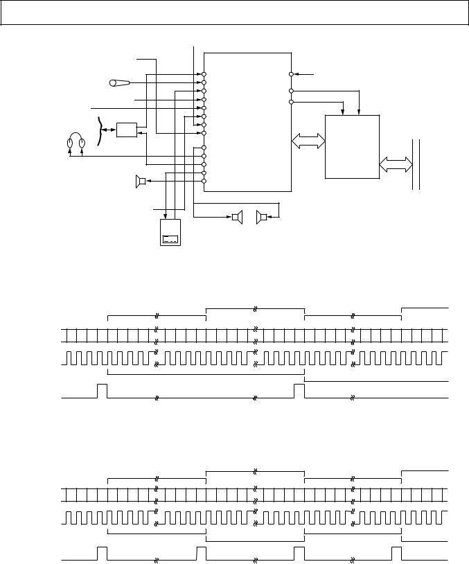
AD1843
|
|
PC ATTENTION |
|
|
|
|
|
“BEEPER” SIGNAL |
|
|
|
|
EXTERNAL |
AD1843 SOUNDCOMM |
|
|
|
|
WAVEFORM |
|
|
||
|
SYNTHESIZER |
CODEC |
NTSC |
|
|
|
|
|
|
|
|
|
|
LINE IN |
SYNC2 |
HORIZONTAL |
|
|
|
MIC IN RIGHT |
|
SYNC SIGNAL |
|
|
|
|
|
|
|
|
AUDIO FROM |
MIC IN LEFT |
CONV1 |
|
|
AUDIO FROM |
AUX1 IN |
|
|
|
|
CD-ROM |
BIT1 |
|
|
||
|
|
|
|||
EXTERNAL MPEG |
|
AUX2 IN |
|
|
|
DECODER |
|
AUX3 IN |
|
|
|
|
|
|
ADSP-21xx |
|
|
|
|
MONO IN |
|
|
|
|
DAA |
|
DSP OR ASIC |
HOST BUS |
|
|
|
|
|||
|
SUM IN |
|
|
||
|
|
SERIAL |
SERIAL |
ISA OR PCI |
|
|
|
|
|||
|
|
|
|
||
|
PSTN |
LINE1 OUT |
INTERFACE |
INTERFACE |
|
|
|
|
|
||
|
|
|
|
|
|
|
|
HEADPHONE OUT |
|
IDMA PORT |
|
|
|
|
|
|
|
|
|
LINE2 OUT RIGHT |
|
OR PARALLEL |
|
|
|
LINE2 OUT LEFT |
|
PORT |
|
|
|
|
|
|
|
|
|
MONO OUT |
|
|
|
|
PC SPEAKER |
|
|
|
|
|
AUDIO FROM DAT |
|
|
|
|
|
OR CASSETTE |
|
|
|
|
|
|
EXTERNAL POWERED |
|
|
|
|
|
MULTIMEDIA SPEAKERS |
|
|
|
|
SPEAKERPHONE |
|
|
|
|
Figure 6. Typical Configurations
|
|
|
|
|
|
|
|
|
|
SAMPLE |
|
|
|
|
SAMPLE PERIOD N+1 |
|
|
|
PERIOD N+3 |
||
|
|
SAMPLE PERIOD N |
SLOT 16 |
|
SLOT 31 |
SAMPLE PERIOD N+2 |
SLOT 16 |
|||
|
SLOT 0 |
|
SLOT 15 |
|
|
SLOT 0 |
|
SLOT 15 |
256 BITS |
|
|
|
|
|
256 BITS |
|
|
|
|
|
|
|
|
256 BITS |
|
|
|
|
256 BITS |
|
|
|
SDI OR SDO |
3 2 1 0 15 14 |
13 12 |
3 2 |
1 0 15 14 13 12 |
3 |
2 1 0 |
15 14 13 12 |
3 |
2 1 0 |
15 14 13 12 |
|
MSB |
|
|
MSB |
|
|
MSB |
|
|
MSB |
SCLK |
|
|
|
|
|
|
|
|
|
|
|
|
|
|
512 BITS |
|
|
|
|
512 BITS |
|
|
|
|
|
FRAME M |
|
|
|
|
|
|
FRAME M+1
SDFS
FRS = 0 [DEFAULT 32 SLOTS PER FRAME, 2 SAMPLES PER FRAME SYNC]
MASTER MODE
NOTE THAT AD1843 FRAME RATE IS NOT RELATED TO SAMPLE RATES
Figure 7. FRS = 0, Master Mode Timing
|
|
|
|
|
|
|
|
|
|
SAMPLE |
|
|
|
|
SAMPLE PERIOD N+1 |
|
|
|
PERIOD N+3 |
||
|
|
SAMPLE PERIOD N |
SLOT 0 |
|
SLOT 15 |
SAMPLE PERIOD N+2 |
SLOT 0 |
|||
|
SLOT 0 |
|
SLOT 15 |
|
|
|
SLOT 0 |
|
SLOT 15 |
|
SDI OR SDO |
3 2 1 0 15 14 |
13 12 |
3 2 1 0 |
15 14 13 12 |
3 |
2 1 0 |
15 14 13 12 |
3 |
2 1 0 |
15 14 13 12 |
|
MSB |
|
|
MSB |
|
|
MSB |
|
|
MSB |
SCLK |
|
|
|
|
|
|
|
|
|
|
|
|
256 BITS |
|
256 BITS |
|
|
256 BITS |
|
|
|
|
|
FRAME M |
|
|
|
|
FRAME M+2 |
|
|
|
|
|
|
|
FRAME M+1 |
|
|
|
|
FRAME M+3 |
|
SDFS |
|
|
|
|
|
|
|
|
|
|
FRS = 1 [16 SLOTS PER FRAME, 1 SAMPLE PER FRAME SYNC]
MASTER MODE
NOTE THAT SCLK CAN BE PROGRAMMED FOR EITHER 12.288 MHz
OR 16.384 MHz WHEN IN MASTER MODE
Figure 8. FRS = 1, Master Mode Timing
REV. 0 |
–17– |
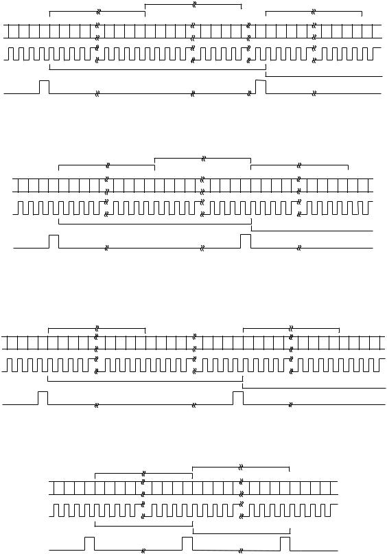
AD1843
|
|
|
SAMPLE PERIOD N+1 |
|
|
|
|||
|
SAMPLE PERIOD N |
SLOT 16 |
|
|
SLOT 31 |
SAMPLE PERIOD N+2 |
|||
|
SLOT 0 |
SLOT 15 |
|
|
256 BITS |
|
SLOT 0 |
|
SLOT 15 |
|
|
|
|
|
|
|
|
|
|
|
GAP |
256 BITS |
|
|
|
|
GAP |
256 BITS |
|
SDI OR SDO |
15 14 13 12 |
3 2 1 0 |
15 14 13 |
12 |
3 |
2 1 0 |
15 14 13 |
12 |
3 2 1 0 15 |
|
MSB |
|
MSB |
|
|
|
MSB |
|
MSB |
SCLK |
|
|
|
|
|
|
|
|
|
|
|
|
512 BITS |
|
|
|
|
|
512 BITS |
FRAME M
FRAME M+1
TSI
FRS = 0 [DEFAULT 32 SLOTS PER FRAME, 2 SAMPLES PER FRAME SYNC]
EXAMPLE SHOWING GAPS BETWEEN FRAMES
SLAVE MODE
Figure 9a. FRS = 0, Slave Mode Timing
|
|
|
|
|
|
|
SAMPLE PERIOD N+1 |
|
|
|
|
|
||
|
|
|
|
SAMPLE PERIOD N |
SLOT 16 |
|
SLOT 31 |
SAMPLE PERIOD N+2 |
||||||
|
|
SLOT 0 |
|
SLOT 15 |
|
256 BITS |
SLOT 0 |
|
|
SLOT 15 |
||||
|
|
|
|
|
|
|
|
|
|
|
|
|
|
|
|
|
|
|
|
256 BITS |
|
|
|
|
|
|
256 BITS |
|
|
SDI OR SDO |
3 2 1 0 |
15 |
14 |
13 12 |
3 |
2 |
1 0 15 14 13 |
12 |
3 2 1 0 |
15 14 |
13 12 |
3 |
2 |
1 0 15 14 |
|
|
MSB |
|
|
|
|
MSB |
|
MSB |
|
|
|
MSB |
|
SCLK |
|
|
|
|
|
|
|
|
|
|
|
|
|
|
|
|
|
|
|
|
|
512 BITS |
|
|
|
|
512 BITS |
||
|
|
|
|
|
|
|
FRAME M |
|
|
|
|
|
|
|
TSI |
|
|
|
|
|
|
|
|
|
|
|
FRAME M+1 |
||
|
|
|
|
|
|
|
|
|
|
|
|
|
|
|
|
|
|
|
|
FRS = 0 [DEFAULT 32 SLOTS PER FRAME, 2 SAMPLES PER FRAME SYNC] |
|
|
|||||||
|
|
|
|
|
|
|
EXAMPLE SHOWING NO GAPS BETWEEN FRAMES |
|
|
|
|
|||
|
|
|
|
|
|
|
|
SLAVE MODE |
|
|
|
|
|
|
|
|
|
|
|
Figure 9b. FRS = 0, Slave Mode Timing |
|
|
|
|
|
||||
|
|
|
SAMPLE PERIOD N |
|
|
|
SAMPLE PERIOD N+1 |
|
|
|||||
|
SLOT 0 |
|
|
|
SLOT 15 |
|
SLOT 0 |
|
SLOT 15 |
|||||
|
GAP |
|
|
|
|
|
|
GAP |
|
|
|
|
GAP |
|
SDI OR SDO |
15 |
14 |
13 |
12 |
3 2 |
1 |
0 |
|
15 |
14 13 |
12 |
3 2 |
1 |
0 |
|
MSB |
|
|
|
|
|
|
MSB |
|
|
|
|
||
SCLK |
|
|
|
|
|
|
|
|
|
|
|
|
|
|
|
|
|
|
|
|
256 BITS |
|
|
|
|
256 BITS |
|
||
|
|
|
|
|
|
FRAME M |
|
|
|
|
|
|
|
|
FRAME M+1
TSI
FRS = 1 [16 SLOTS PER FRAME, 1 SAMPLES PER FRAME SYNC]
EXAMPLE SHOWING GAPS BETWEEN FRAMES
SLAVE MODE
SDI OR SDO
SCLK
TSI
Figure 10a. FRS = 1, Slave Mode Timing
|
|
|
|
|
|
SAMPLE PERIOD N |
|
|
|
SAMPLE PERIOD N+1 |
|
|
|
|
|
|
|||||||
|
|
|
|
|
|
|
|
SLOT 0 |
|
|
|
SLOT 15 |
|
|
|
|
|||||||
|
|
|
|
SLOT 0 |
|
|
|
SLOT 15 |
|
|
|
|
|
|
|
|
|
|
|
|
|||
3 |
2 |
1 |
0 |
15 |
14 |
13 |
12 |
3 |
2 |
1 |
0 |
15 |
14 |
13 |
12 |
3 |
2 |
1 |
0 |
15 |
14 |
13 |
12 |
|
|
|
|
MSB |
|
|
|
|
|
|
|
MSB |
|
|
|
|
|
|
|
MSB |
|
|
|
|
|
|
|
|
|
|
|
256 BITS |
|
|
|
|
|
|
256 BITS |
|
|
|
|
|
|
||
|
|
|
|
|
|
|
FRAME M |
|
|
|
|
|
|
|
|
|
|
|
|
|
|
|
|
|
|
|
|
|
|
|
|
|
|
|
|
|
|
|
FRAME M+1 |
|
|
|
|
|
|
|
|
FRS = 1 [16 SLOTS PER FRAME, 1 SAMPLES PER FRAME SYNC]
EXAMPLE SHOWING NO GAPS BETWEEN FRAMES
SLAVE MODE
Figure 10b. FRS = 1, Slave Mode Timing
–18– |
REV. 0 |

AD1843
Modem Data Access Arrangement (DAA) devices are generally differential on the transmit side, and single-ended on the receive side. The DAA transmit input (generally differential) should be connected to the DAC2 output, pins LOUT2LP and LOUT2LN, or LOUT2RP and LOUT2RN. The DAA receive output (generally single-ended) should be connected to one of the ADC line inputs, LINLP or LINRP. See the “APPLICATION CIRCUITS” section below for more detail on the electrical connections. There are several software driver steps that are required to configure the SoundComm codec for use as a modem AFE.
Configure DAC2
1.Set the DA2FLT bit (Control Register Address 25, Bit 9) to “1,” to select the digital modem filter mode. The DAC2 outputs can be used either as differential outputs or single-ended outputs depending on how the pins are connected electrically; no Control Register writes are required to configure the DAC2 outputs as either differential or single-ended.
2.Program LDA2G5:0 (Control Register Address 10, Bits 8 through 13) to “00 0101” (i.e., +4.5 dB) or RDA2G5:0 (Control Register 10, Bits 0 through 5) to “00 0101” (i.e., +4.5 dB), depending on whether the DAA transmit input is connected to the left channel DAC2 output (use LDA2G5:0) or the right channel DAC2 output (use RDA2G5:0). This code establishes the DAC2 nominal analog output swing at 3.156 V p-p single-ended, or 6.312 V p-p differentially. The 3.156 V p-p level is equivalent to 3.17 dBm.
Configure ADC
1.Set the ADLFLT bit (Control Register Address 25, Bit 0) to “1,” or the ADRFLT bit (Control Register Address 25, Bit 1) to “1,” to select the digital modem filter mode. Set ADLFLT if the DAA receive output is connected to the AD1843 LINLP input; set ADRFLT if the DAA receive output is connected to the AD1843 LINRP input. Set the LINLSD bit (Control Register Address 28, Bit 0) to “1” if the DAA is connected to the AD1843 LINLP input; set the LINRSD bit (Control Register Address 28, Bit 1) to “1” if the DAA is connected to the AD1843 LINRP input.
2.Program LIG3:0 (Control Register Address 2, Bits 8 through 11) to “0000” (i.e., 0.0 dB) or RIG3:0 (Control Register Address 2, Bits 0 through 3) to “0000” (i.e., 0.0 dB) depending on whether the left or right ADC input channel is being used for the modem function. This code maps an ana-
log input swing of 3.156 V p-p to the full dynamic range of the 16-bit digital sample (i.e., ±215). The 3.156 V p-p level is equivalent to 3.17 dBm.
Note that if the AD1843 is to be reconfigured dynamically, the affected converter must be powered down before its associated digital filter can be changed. In other words, if the digital filter for the ADC left channel is being changed from audio mode to modem mode, the ADC left channel must be powered down first (using the ADLEN bit in Control Register Address 27).
Use the ADREN bit in Control Register Address 27 for the ADC right channel, the DAC1EN bit in Control Register Address 27 for DAC1, and the DAC2EN bit in Control Register Address 27 for DAC2.
Typical Configurations
Figure 6 below illustrates example connections between the AD1843 SoundComm codec and other system resources. The rich analog input and output connectivity of the AD1843 allows a wide variety of configuration possibilities. Note that the level of modem, speakerphone and external speaker concurrency is application and DSP resource dependent.
SERIAL INTERFACE
The AD1843 SoundComm Codec transmits and receives both data and control/status information through its serial port.
The AD1843 can be configured as either master or slave of the serial interface. This is selected by using the BM pin. When BM is tied HI, the AD1843 serves as bus master and supplies the frame sync and the serial clock. When BM is tied LO, the AD1843 serves as bus slave and receives the frame sync and the serial clock. The level on BM should not be altered unless the reset pin (RESET) is asserted.
The AD1843 has six pins devoted to the serial interface: SDI, SDO, SCLK, SDFS, TSI and TSO. The SDI pin is for serial data input to the AD1843 and the SDO pin is for serial data output from the AD1843. The SCLK pin is the serial interface clock. Communication in and out of the AD1843 requires bits of data to be transmitted after a rising edge of SCLK, and sampled on a falling edge of SCLK. When the AD1843 is bus master (BM pin tied HI), the SCLK frequency driven by the AD1843 will be 12.288 MHz by default, but this can be increased to 16.384 MHz by setting the SCF bit in Control Register 26. When the AD1843 is bus slave (BM pin tied LO), the SCLK frequency driven to the AD1843 may be as high as 24.576 MHz, but must not be any higher than the frequency on the XTALI pin.
The SDFS pin is for the serial interface frame sync. When bus master, new frames are marked by a HI pulse driven out on SDFS one serial clock period before the frame begins. When bus slave, new frames must be marked by a LO to HI transition driven in on SDFS one serial clock period before the frame begins, but the transition back from HI to LO may occur at any time provided the HI and LO times of SDFS are at least one SCLK period in duration each.
When the AD1843 is bus master, frame size is controlled by the FRS bit in Control Register 26. When FRS is set to “1,” each frame is divided into 16 slots of 16 bits. When FRS is reset to “0,” each frame is divided into 32 slots of 16 bits. In 32 slot configuration, the second 16 slots of a frame must have slot assignments that are identical to the first 16 slots of the frame; 32 slot configuration is essentially 16 slot configuration with every other SDFS pulse missing. Although these are the frame sizes
REV. 0 |
–19– |
AD1843
produced by an AD1843 serving as bus master, an AD1843 serving as bus slave does not actually require these frame sizes. When FRS is set to “1,” a slave will operate correctly with any number or fraction of slots, provided there are enough slots for it to complete its necessary communication (see below). When FRS is reset to “0,” a slave can also operate correctly with a wide range in the number of slots per frame, however it will automatically retake ownership of the serial interface bus 16 slots after it is first given ownership of the bus in a frame.
The nominal minimum number of slots when the AD1843 is configured in slave mode is six. The codec must be supplied with at least 6 × 16 = 96 SCLK periods (both rising and falling edges); SCLK may be gated (i.e., no need to be continuous) between valid slots.
While SDFS marks the beginning of frames, AD1843 bus ownership during a frame is controlled by the TSI (Time Slot In) and TSO (Time Slot Out) pins. When bus slave, a level HI on TSI grants the AD1843 bus ownership beginning with the next SCLK period. The TSI pin is monitored only when an AD1843 does not already own the bus; once an AD1843 is given ownership of the bus, the level on TSI is ignored until one SCLK period before bus ownership is relinquished. Bus ownership will last for six slots. Coincident with the final SCLK period of the final slot owned, the AD1843 asserts TSO HI. This allows chaining of AD1843s onto a common serial bus by connecting the TSO pin of one AD1843 to the TSI pin on the next later AD1843 in a chain. In single codec systems where the SoundComm is configured as bus slave, connect the AD1843 SDFS and TSI signals together. When an AD1843 is bus master, its function is identical to that just described for the slave, except a bus master always owns the first six slots and its TSI pin is ignored (but should be tied LO).
Whenever an AD1843 does not own the bus, its SDO pin will be three-stated and its SDI pin is ignored. Figures 7 through 10 illustrate the signal, slot, sample and frame relationships for the four basic operating modes of the AD1843 serial interface.
The AD1843 requires slots of communication each time it takes ownership of the serial bus. The first slot is used for a Control Word input and a Status Word output. The second slot is used
for Control Register write data input and read data output. The remaining slots are used for playback (DAC) data input and capture (ADC) data output, where each channel has an assigned slot. Table II and Figure 11 illustrate these slot assignments.
Since the conversion channels of the AD1843 can be programmed to run at different sample rates, a communication mechanism indicates when playback channels request data, when playback data is actually sent to the AD1843, and when transmission of capture data from the AD1843 becomes necessary. This is facilitated by the Control and Status Words located in the first slot. The Control Word indicates which slots in the current frame contain valid playback data. The Status Word indicates if playback data can be sent to the AD1843 during the next frame, and which slots in the current frame contain valid capture data. See the descriptions of the Control Word and the Status Word below for additional detail.
Four word FIFO buffers are used on the inputs of each of the DACs to allow data to be transferred in small bursts. This reduces the required response time to playback data requests, and also buffers differences between the frame sync rate and the channel sample rate. The Status Word indicates that playback data can be sent if there is any room in the buffers, thus tending to keep the input buffers full. Underrun flags are available in Control Register 1, which indicate if an input buffer ran out of data. If an underrun occurs, a zero is used in place of the unavailable data. To ensure underruns do not occur, playback data must be sent to the AD1843 within two sample periods after the status word indicates that the DAC FIFO is not full.
Note that the DAC Not Full status bits (DA2RQ and DA1RQ in the Status Word Output) are updated immediately (i.e., in the same frame as a valid write to the DAC FIFOs). If the DAC Input Valid Flags (DA2V and DA1V in the Control Word Input) are set (i.e., DAC data is valid) and only one location in the DAC1 and DAC2 input FIFOs is available, then the DA2RQ and DA1RQ status bits will reflect this valid write, and will be reset to “0.” This is possible because the DA2V and DA1V bits are in the most significant bits of the Control Word and the DA2RQ and DA1RQ bits are in the least significant bits of the Status Word, and the AD1843 uses this intervening time
Table II. AD1843 Slot Assignment
32 Slot Mode (FRS Reset to “0”)
Slot |
SDI Pin |
SDO Pin |
|
|
|
0 & 16 |
Control Word Input |
Status Word Output |
1 & 17 |
Control Register Data Input |
Control Register Data Output |
2 & 18 |
Playback Data Input—DAC1 Left |
Capture Data Output—ADC Left |
3 & 19 |
Playback Data Input—DAC1 Right |
Capture Data Output—ADC Right |
4 & 20 |
Playback Data Input—DAC2 Left |
Reserved (Unused) |
5 & 21 |
Playback Data Input—DAC2 Right |
Reserved (Unused) |
|
|
|
16 Slot Mode (FRS Set to “1”) |
|
|
|
|
|
Slot |
SDI Pin |
SDO Pin |
|
|
|
0 |
Control Word Input |
Status Word Output |
1 |
Control Register Data Input |
Control Register Data Output |
2 |
Playback Data Input—DAC1 Left |
Capture Data Output—ADC Left |
3 |
Playback Data Input—DAC1 Right |
Capture Data Output—ADC Right |
4 |
Playback Data Input—DAC2 Left |
Reserved (Unused) |
5 |
Playback Data Input—DAC2 Right |
Reserved (Unused) |
|
|
|
–20– |
REV. 0 |
 Loading...