


 Loading...
a |
Quad Low Power, |
|
Precision Comparator |
||
|
|
|
|
|
CMP04 |
|
|
|
FEATURES
High Gain: 200 V/mV typ
Single or Dual Supply Operation Input Voltage Range Includes Ground
Low Power Consumption (1.5 mW/Comparator) Low Input Bias Current: 100 nA max
Low Input Offset Current: 10 nA max Low Offset Voltage: 1 mV max
Low Output Saturation Voltage: 250 mV @ 4 mA
Logic Output Compatible with TTL, DTL, ECL, MOS and CMOS
Directly Replaces LM139/239/339 Comparators Available in Die Form
PIN CONNECTIONS
14-Lead Cerdip
14-Lead Plastic DIP
14-Lead SOIC
OUT 2 |
1 |
|
|
14 |
OUT 3 |
OUT 1 |
2 |
|
|
13 |
OUT 4 |
V+ |
3 |
1 |
4 |
12 |
GND |
IN 1– 4 |
|
|
11 |
IN 4+ |
|
IN 1+ |
5 |
|
|
10 |
IN 4– |
IN 2– 6 |
2 |
3 |
9 |
IN 3+ |
|
IN 2+ |
7 |
CMP04 |
8 |
IN 3– |
|
|
|
|
|
||
GENERAL DESCRIPTION
Four precision independent comparators comprise the CMP04. Performance highlights include a very low offset voltage, low output saturation voltage and high gain in a single supply design. The input voltage range includes ground for single supply operation and V– for split supplies. A low power supply current of 2 mA, which is independent of supply voltage, makes this the preferred comparator for precision applications requiring minimal power consumption. Maximum logic interface flexibility is offered by the open-collector TTL output.
TYPICAL INTERFACE
|
|
5.0 |
|
3 |
100kV |
1/4 |
|
CD4011 |
|||
|
1/4
CMP04
12
Figure 2a. Driving CMOS
|
|
V+ |
|
|
|
|
|
|
|
|
|
|
|
|
5.0 |
|
3.5mA |
100mA |
3.5mA |
|
100mA |
|
|
|
|
|
|
|
OUTPUT |
3 |
10kV |
|
|
|
|
|
|
|
|
|
Q2 |
Q3 |
|
|
Q8 |
1/4 |
|
|
|
|
|
CMP04 |
|
||
+INPUT |
Q1 |
|
Q4 |
|
–INPUT |
12 |
1/4 SN7400 |
|
* |
|
|
|
* |
|
|
|
|
|
Q7 |
|
|
||
|
|
|
|
|
|
|
|
|
Q5 |
Q6 |
|
|
|
Figure 2b. Driving TTL |
|
*SUBSTRATE DIODES |
|
|
|
|
|||
|
|
|
|
|
|
||
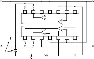
Figure 1. Simplified Schematic (1/4 CMP04)
REV. C
Information furnished by Analog Devices is believed to be accurate and reliable. However, no responsibility is assumed by Analog Devices for its use, nor for any infringements of patents or other rights of third parties which may result from its use. No license is granted by implication or otherwise under any patent or patent rights of Analog Devices.
One Technology Way, P.O. Box 9106, Norwood, MA 02062-9106, U.S.A.
Tel: 781/329-4700 |
World Wide Web Site: http://www.analog.com |
Fax: 781/326-8703 |
© Analog Devices, Inc., 1998 |

CMP04–SPECIFICATIONS
ELECTRICAL CHARACTERISTICS |
(@ V+ = +5 V, TA = +258C, unless otherwise noted) |
|
|
|
|||
Parameter |
Symbol |
|
Conditions |
Min |
Typ |
Max |
Units |
|
|
|
|
|
|
|
|
Input Offset Voltage |
VOS |
|
RS = 0 Ω, RL = 5.1 kΩ, VO = 1.4 V1 |
|
0.4 |
1 |
mV |
Input Offset Current |
IOS |
|
IIN(+) – IIN(–), RL = 5.1 kΩ, VO = 1.4 V |
|
2 |
10 |
nA |
Input Bias Current |
IB |
|
IIN(+) or IIN(–) |
|
25 |
100 |
nA |
Voltage Gain |
AV |
|
RL ≥ 15 kΩ, V+ = 15 V2 |
80 |
200 |
|
V/mV |
Large-Signal Response Time |
tr |
|
VIN = TTL Logic Swing, VREF = 1.4 V3 |
|
|
|
|
|
|
|
VRL = 5 V, RL = 5.1 kΩ |
|
300 |
|
ns |
Small-Signal Response Time |
tr |
|
VIN = 100 mV Step3, 5 mV Overdrive |
|
|
|
|
|
|
|
VRL = 5 V, RL = 5.1 kΩ |
|
1.3 |
|
µs |
Input Voltage Range |
CMVR |
|
(Note 4) |
0 |
|
V+ –1.5 |
V |
Common-Mode Rejection Ratio |
CMRR |
|
(Notes 2, 5) |
80 |
100 |
|
dB |
Power Supply Rejection Ratio |
PSRR |
|
V+ = +5 V to +18 V2 |
80 |
100 |
|
dB |
Saturation Voltage |
VOL |
|
VIN(–) ≥ 1 V, VIN(+) = 0, ISINK ≤ 4 mA |
|
250 |
400 |
mV |
Output Sink Current |
ISINK |
|
VIN(–) ≥ 1 V, VIN(+) = 0, VO ≤ 1.5 V |
6 |
16 |
|
mA |
Output Leakage Current |
ILEAK |
|
VIN(+) ≥ 1 V, VIN(–) = 0, VO = 30 V |
|
0.1 |
100 |
nA |
Supply Current |
I+ |
|
RL = ∞, All Comps V+ = 30 V |
|
0.8 |
2.0 |
mA |
NOTES
1At output switch point, VO = 1.4 V, RS = 0 Ω with V+ from 5 V; and over the full input common-mode range (0 V to V+ –1.5 V). 2Guaranteed by design.
3Sample tested.
4The input common-mode voltage or input signal voltage should not be allowed to go negative by more than 0.3 V. The upper end of the common-mode voltage range is V+ –1.5 V, but either or both inputs can go to +30 V without damage.
5RL ≥ 15 kΩ, V+ = 15 V, VCM = 1.5 V to 13.5 V.
Specifications subject to change without notice.
ABSOLUTE MAXIMUM RATINGS1 |
36 V or ±18 V |
Supply Voltage . . . . . . . . . . . . . . . . . . . . . . . |
|
Differential Input Voltage . . . . . . . . . . . . . . . |
. . . . . . . 36 V dc |
Input Voltage . . . . . . . . . . . . . . . . . . . . . . . . . |
–0.3 V to +36 V |
Operating Temperature Range |
–55°C to +125°C |
CMP04BY . . . . . . . . . . . . . . . . . . . . . . . . |
|
CMP04FP, FS . . . . . . . . . . . . . . . . . . . . . . |
–40°C to +85°C |
Junction Temperature (TJ) . . . . . . . . . . . . . |
–65°C to +150°C |
Storage Temperature Range . . . . . . . . . . . . |
–65°C to +150°C |
(P Suffix) . . . . . . . . . . . . . . . . . . . . . . . . . |
–65°C to +125°C |
Input Current (VIN < –3.0 V) . . . . . . . . . . . . |
. . . . . . . 50 mA |
Output Short-Circuit to GND . . . . . . . . . . . . |
. . . . Continuous |
Lead Temperature (Soldering, 60 sec) . . . . . |
. . . . . . .+300°C |
Package Type |
uJA2 |
uJC |
Units |
14-Lead Hermetic DIP (Y) |
94 |
10 |
°C/W |
14-Lead Plastic DIP (P) |
83 |
39 |
°C/W |
14-Lead SOIC |
120 |
36 |
°C/W |
|
|
|
|
NOTES
1Absolute maximum ratings apply to both DICE and packaged parts, unless otherwise noted. Stresses above those listed under Absolute Maximum Ratings may cause permanent damage to the device. This is a stress rating only; functional operation of the device at these or any other conditions above those listed in the operational sections of this specification is not implied. Exposure to absolute maximum rating conditions for extended periods may affect device reliability.
2θJA is specified for worst case mounting conditions, i.e., θJA is specified for device in socket for cerdip and plastic DIP packages; θJA is specified for device soldered to printed circuit board for SO package.
ORDERING GUIDE
|
TA = +258C |
Temperature |
Package |
Package |
Model |
VOS |
Ranges |
Descriptions |
Options |
CMP04BY/883C |
1 mV |
–55°C to +125°C |
14-Lead Cerdip |
Q-14 |
CMP04FP |
1 mV |
–40°C to +85°C |
14-Lead Plastic DIP |
N-14 |
CMP04FS |
1 mV |
–40°C to +85°C |
14-Lead SOIC |
R-14/SO-14 |
CAUTION
ESD (electrostatic discharge) sensitive device. Electrostatic charges as high as 4000 V readily accumulate on the human body and test equipment and can discharge without detection. Although the CMP04 features proprietary ESD protection circuitry, permanent damage may occur on devices subjected to high energy electrostatic discharges. Therefore, proper ESD precautions are recommended to avoid performance degradation or loss of functionality.
WARNING!
ESD SENSITIVE DEVICE
–2– |
REV. C |
|
|
|
|
|
|
|
CMP04 |
|
ELECTRICAL CHARACTERISTICS |
(@ V+ = +5 V, –558C ≤ TA ≤ +1258C for CMP04BY, –408C ≤ TA ≤ +858C for |
|
|
|||||
CMP04FP/FS, unless otherwise noted) |
|
|
|
|
||||
|
|
|
|
|
|
|
|
|
|
|
|
|
|
CMP04B/F1 |
|
|
|
Parameter |
Symbol |
|
Conditions |
Min |
Typ |
Max |
Units |
|
|
|
|
|
|
|
|
|
|
Input Offset Voltage |
VOS |
|
RS = 0 Ω, RL = 5.1 kΩ |
|
1 |
2 |
mV |
|
|
|
|
VO = 1.4 V2 |
|
1 |
2 |
mV |
|
Input Offset Current |
IOS |
|
IIN(+) – IIN(–) |
|
4 |
20 |
nA |
|
|
|
|
RL = 5.1 kΩ |
|
4 |
20 |
nA |
|
|
|
|
VO = 1.4 V |
|
4 |
20 |
nA |
|
Input Bias Current |
IB |
|
IIN(+) or IIN(–) |
|
40 |
200 |
nA |
|
|
|
|
|
|
|
|
|
|
Voltage Gain |
AV |
|
RL ≥ 15 kΩ, V+ = 15 V3 |
70 |
125 |
|
V/mV |
|
Large-Signal Response Time |
tr |
|
VIN = TTL Logic Swing |
|
300 |
|
ns |
|
|
|
|
VREF = 1.4 V4 |
|
300 |
|
ns |
|
|
|
|
VRL = 5 V, RL = 5.1 kΩ |
|
300 |
|
ns |
|
Small-Signal Response Time |
tr |
|
VIN = 100 mV Step4 |
|
1.3 |
|
µs |
|
|
|
|
5 mV Overdrive |
|
1.3 |
|
µs |
|
|
|
|
VRL = 5 V, RL = 5.1 kΩ |
|
1.3 |
|
µs |
|
Input Voltage Range |
CMVR |
|
(Note 5) |
0 |
|
V+ –1.5 |
V |
|
|
|
|
|
|
|
|
|
|
Common-Mode Rejection Ratio |
CMRR |
|
(Notes 1, 3) |
60 |
100 |
|
dB |
|
|
|
|
|
|
|
|
|
|
Power Supply Rejection Ratio |
PSRR |
|
V+ = +5 V to +18 V |
80 |
100 |
|
dB |
|
|
|
|
|
|
|
|
|
|
Saturation Voltage |
VOL |
|
VIN(–) ≥ 1 V, VIN(+) = 0, |
|
250 |
700 |
mV |
|
|
|
|
ISINK ≤ 4 mA |
|
250 |
700 |
mV |
|
Output Sink Current |
ISINK |
|
VIN(–) ≥ 1 V, |
5 |
16 |
|
mA |
|
|
|
|
VIN(+) = 0, VO ≤ 1.5 V |
5 |
16 |
|
mA |
|
Output Leakage Current |
ILEAK |
|
VIN(+) ≥ 1 V, |
|
0.1 |
200 |
nA |
|
|
|
|
VIN(–) = 0, VO = 30 V |
|
0.1 |
200 |
nA |
|
Supply Current |
I+ |
|
RL = ∞, All Comps |
|
1.2 |
3.0 |
mA |
|
|
|
|
V+ = 30 V |
|
1.2 |
3.0 |
mA |
|
|
|
|
|
|
|
|
|
|
NOTES
1RL ≥ 15 kΩ, V+ = 15 V, VCM = 1.5 V to 13.5 V.
2At output switch point, VO = 1.4 V, RS = 0 Ω with V+ from 5 V; and over the full input common-mode range (0 V to V+ –1.5 V). 3Guaranteed by design.
4Sample tested.
5The input common-mode voltage or input signal voltage should not be allowed to go negative by more than 0.3 V. The upper end of the common-mode voltage range is V+ –1.5 V, but either or both inputs can go to +30 V without damage.
Specifications subject to change without notice.
–18V |
|
|
|
|
|
|
–18V |
|
3.6kV |
|
3.6kV |
|
|
|
|
|
14 |
13 |
12 |
11 |
10 |
9 |
8 |
|
|
|
|
4 |
|
|
|
|
|
|
|
|
|
1 |
|
|
|
|
CMP04 |
|
|
|
|
|
|
|
|
|
|
2 |
|
|
|
|
|
3 |
|
|
|
100kV |
1 |
2 |
3 |
4 |
5 |
6 |
7 |
|
|
|
|
|
|
|
|
|
3.6kV |
|
3.6kV |
|
|
|
|
+18V |
ZENER |
|
|
|
|
|
+18V |
|
|
|
|
|
|
|
|
ONE EACH |
5.8V TO 6.2V |
|
470kV |
|
|
|
|
1 WATT |
|
|
|
|
|
||
PER BOARD |
|
|
|
|
|
|
|
+30V |
MIL-STD-883, METHOD 1015, CONDITION B |
TO ADJACENT SOCKETS |
|
Figure 3. Burn-In Circuit
REV. C |
–3– |
Loading...