


a |
Low Cost, Low Power |
|
Instrumentation Amplifier |
||
|
|
|
|
|
AD620 |
|
|
|
FEATURES EASY TO USE
Gain Set with One External Resistor (Gain Range 1 to 1000)
Wide Power Supply Range (62.3 V to 618 V)
Higher Performance than Three Op Amp IA Designs Available in 8-Lead DIP and SOIC Packaging
Low Power, 1.3 mA max Supply Current
EXCELLENT DC PERFORMANCE (“B GRADE”) 50 mV max, Input Offset Voltage
0.6 mV/8C max, Input Offset Drift
1.0 nA max, Input Bias Current
100 dB min Common-Mode Rejection Ratio (G = 10)
LOW NOISE
9 nV/ÖHz, @ 1 kHz, Input Voltage Noise 0.28 mV p-p Noise (0.1 Hz to 10 Hz)
EXCELLENT AC SPECIFICATIONS 120 kHz Bandwidth (G = 100)
15 ms Settling Time to 0.01%
APPLICATIONS
Weigh Scales
ECG and Medical Instrumentation
Transducer Interface
Data Acquisition Systems
Industrial Process Controls
Battery Powered and Portable Equipment
PRODUCT DESCRIPTION
The AD620 is a low cost, high accuracy instrumentation amplifier that requires only one external resistor to set gains of 1 to
CONNECTION DIAGRAM
8-Lead Plastic Mini-DIP (N), Cerdip (Q)
and SOIC (R) Packages
RG |
1 |
|
8 |
RG |
–IN |
2 |
|
7 |
+VS |
+IN |
3 |
|
6 |
OUTPUT |
–V |
4 |
AD620 |
5 |
REF |
S |
|
TOP VIEW
1000. Furthermore, the AD620 features 8-lead SOIC and DIP packaging that is smaller than discrete designs, and offers lower power (only 1.3 mA max supply current), making it a good fit for battery powered, portable (or remote) applications.
The AD620, with its high accuracy of 40 ppm maximum nonlinearity, low offset voltage of 50 mV max and offset drift of 0.6 mV/°C max, is ideal for use in precision data acquisition systems, such as weigh scales and transducer interfaces. Furthermore, the low noise, low input bias current, and low power of the AD620 make it well suited for medical applications such as ECG and noninvasive blood pressure monitors.
The low input bias current of 1.0 nA max is made possible with the use of Superbeta processing in the input stage. The AD620 works well as a preamplifier due to its low input voltage noise of 9 nV/ÖHz at 1 kHz, 0.28 mV p-p in the 0.1 Hz to 10 Hz band, 0.1 pA/ÖHz input current noise. Also, the AD620 is well suited for multiplexed applications with its settling time of 15 ms to 0.01% and its cost is low enough to enable designs with one inamp per channel.
|
30,000 |
|
|
|
|
SCALE |
25,000 |
|
|
3 OP-AMP |
|
|
|
|
IN-AMP |
|
|
|
|
|
(3 OP-07s) |
|
|
OF FULL |
|
|
|
|
|
20,000 |
|
|
|
|
|
|
|
|
|
|
|
PPM |
15,000 |
|
|
|
|
|
AD620A |
|
|
|
|
ERROR, |
|
|
|
|
|
10,000 |
RG |
|
|
|
|
|
|
|
|
||
TOTAL |
5,000 |
|
|
|
|
|
|
|
|
|
|
|
0 |
|
|
|
|
|
0 |
5 |
10 |
15 |
20 |
|
|
|
SUPPLY CURRENT – mA |
|
|
Figure 1. Three Op Amp IA Designs vs. AD620
10,000 |
|
|
|
|
|
|
|
1,000 |
|
|
|
|
|
VOLTAGE NOISE – 10Hz) –mV p-p |
|
|
TYPICAL STANDARD |
|
|
|
|
|
BIPOLAR INPUT |
|
|
|
|
100 |
|
IN-AMP |
|
|
|
|
|
|
|
|
|
||
|
G = 100 |
|
|
|
||
10 |
|
|
|
|
|
|
RTI (0.1 |
|
|
|
|
AD620 SUPERbETA |
|
|
|
|
|
|
|
|
|
1 |
|
|
|
BIPOLAR INPUT |
|
|
|
|
|
IN-AMP |
|
|
|
0.1 |
|
|
|
|
|
|
1k |
10k |
100k |
1M |
10M |
100M |
|
|
|
SOURCE RESISTANCE –V |
|
||
Figure 2. Total Voltage Noise vs. Source Resistance
REV. E
Information furnished by Analog Devices is believed to be accurate and reliable. However, no responsibility is assumed by Analog Devices for its use, nor for any infringements of patents or other rights of third parties which may result from its use. No license is granted by implication or otherwise under any patent or patent rights of Analog Devices.
One Technology Way, P.O. Box 9106, Norwood, MA 02062-9106, U.S.A.
Tel: 781/329-4700 |
World Wide Web Site: http://www.analog.com |
Fax: 781/326-8703 |
© Analog Devices, Inc., 1999 |
AD620–SPECIFICATIONS |
(Typical @ +258C, VS = 615 V, and RL = 2 kV, unless otherwise noted) |
|
|||||||||
|
|
AD620A |
|
AD620B |
|
|
AD620S1 |
|
|||
Model |
Conditions |
Min |
Typ |
Max |
Min |
Typ |
Max |
Min |
Typ |
Max |
Units |
|
|
|
|
|
|
|
|
|
|
|
|
GAIN |
G = 1 + (49.4 k/RG) |
|
|
|
|
|
|
|
|
|
|
Gain Range |
VOUT = ± 10 V |
1 |
|
10,000 |
1 |
|
10,000 |
1 |
|
10,000 |
|
Gain Error2 |
|
|
|
|
|
|
|
|
|
|
|
G = 1 |
|
|
0.03 |
0.10 |
|
0.01 |
0.02 |
|
0.03 |
0.10 |
% |
G = 10 |
|
|
0.15 |
0.30 |
|
0.10 |
0.15 |
|
0.15 |
0.30 |
% |
G = 100 |
|
|
0.15 |
0.30 |
|
0.10 |
0.15 |
|
0.15 |
0.30 |
% |
G = 1000 |
|
|
0.40 |
0.70 |
|
0.35 |
0.50 |
|
0.40 |
0.70 |
% |
Nonlinearity, |
VOUT = –10 V to +10 V, |
|
|
|
|
|
|
|
|
|
|
G = 1–1000 |
RL = 10 kΩ |
|
10 |
40 |
|
10 |
40 |
|
10 |
40 |
ppm |
G = 1–100 |
RL = 2 kΩ |
|
10 |
95 |
|
10 |
95 |
|
10 |
95 |
ppm |
Gain vs. Temperature |
|
|
|
|
|
|
|
|
|
|
ppm/°C |
|
G =1 |
|
|
10 |
|
|
10 |
|
|
10 |
|
|
Gain >12 |
|
|
–50 |
|
|
–50 |
|
|
–50 |
ppm/°C |
VOLTAGE OFFSET |
(Total RTI Error = VOSI + VOSO/G) |
|
|
|
|
|
|
|
|
|
|
Input Offset, VOSI |
VS = ±5 V to ±15 V |
|
30 |
125 |
|
15 |
50 |
|
30 |
125 |
μV |
|
|
|
|||||||||
Over Temperature |
VS = ±5 V to ±15 V |
|
|
185 |
|
|
85 |
|
|
225 |
μV |
Average TC |
VS = ±5 V to ±15 V |
|
0.3 |
1.0 |
|
0.1 |
0.6 |
|
0.3 |
1.0 |
μV/°C |
Output Offset, VOSO |
VS = ±15 V |
|
400 |
1000 |
|
200 |
500 |
|
400 |
1000 |
μV |
|
VS = ±5 V |
|
|
1500 |
|
|
750 |
|
|
1500 |
μV |
Over Temperature |
VS = ±5 V to ±15 V |
|
|
2000 |
|
|
1000 |
|
|
2000 |
μV |
Average TC |
VS = ± 5 V to ±15 V |
|
5.0 |
15 |
|
2.5 |
7.0 |
|
5.0 |
15 |
μV/°C |
Offset Referred to the |
|
|
|
|
|
|
|
|
|
|
|
Input vs. |
VS = ±2.3 V to ±18 V |
|
|
|
|
|
|
|
|
|
|
Supply (PSR) |
|
|
|
|
|
|
|
|
|
|
|
G = 1 |
|
80 |
100 |
|
80 |
100 |
|
80 |
100 |
|
dB |
G = 10 |
|
95 |
120 |
|
100 |
120 |
|
95 |
120 |
|
dB |
G = 100 |
|
110 |
140 |
|
120 |
140 |
|
110 |
140 |
|
dB |
G = 1000 |
|
110 |
140 |
|
120 |
140 |
|
110 |
140 |
|
dB |
|
|
|
|
|
|
|
|
|
|
|
|
INPUT CURRENT |
|
|
|
|
|
|
|
|
|
|
|
Input Bias Current |
|
|
0.5 |
2.0 |
|
0.5 |
1.0 |
|
0.5 |
2 |
nA |
Over Temperature |
|
|
|
2.5 |
|
|
1.5 |
|
|
4 |
nA |
Average TC |
|
|
3.0 |
|
|
3.0 |
|
|
8.0 |
|
pA/°C |
Input Offset Current |
|
|
0.3 |
1.0 |
|
0.3 |
0.5 |
|
0.3 |
1.0 |
nA |
Over Temperature |
|
|
|
1.5 |
|
|
0.75 |
|
|
2.0 |
nA |
Average TC |
|
|
1.5 |
|
|
1.5 |
|
|
8.0 |
|
pA/°C |
|
|
|
|
|
|
|
|
|
|
|
|
INPUT |
|
|
|
|
|
|
|
|
|
|
|
Input Impedance |
|
|
|
|
|
|
|
|
|
|
GΩipF |
Differential |
|
|
10i2 |
|
|
10i2 |
|
|
10i2 |
|
|
Common-Mode |
VS = ±2.3 V to ±5 V |
|
10i2 |
|
|
10i2 |
|
|
10i2 |
|
GΩipF |
Input Voltage Range3 |
–VS + 1.9 |
|
+VS – 1.2 |
–VS + 1.9 |
|
+VS – 1.2 |
–VS + 1.9 |
|
+VS – 1.2 |
V |
|
Over Temperature |
VS = ±5 V to ±18 V |
–VS + 2.1 |
|
+VS – 1.3 |
–VS + 2.1 |
|
+VS – 1.3 |
–VS + 2.1 |
|
+VS – 1.3 |
V |
|
–VS + 1.9 |
|
+VS – 1.4 |
–VS + 1.9 |
|
+VS – 1.4 |
–VS + 1.9 |
|
+VS – 1.4 |
V |
|
Over Temperature |
|
–VS + 2.1 |
|
+VS – 1.4 |
–VS + 2.1 |
|
+VS – 1.4 |
–VS + 2.3 |
|
+VS – 1.4 |
V |
Common-Mode Rejection |
|
|
|
|
|
|
|
|
|
|
|
Ratio DC to 60 Hz with |
|
|
|
|
|
|
|
|
|
|
|
I kΩ Source Imbalance |
VCM = 0 V to ±10 V |
|
|
|
|
|
|
|
|
|
|
G = 1 |
|
73 |
90 |
|
80 |
90 |
|
73 |
90 |
|
dB |
G = 10 |
|
93 |
110 |
|
100 |
110 |
|
93 |
110 |
|
dB |
G = 100 |
|
110 |
130 |
|
120 |
130 |
|
110 |
130 |
|
dB |
G = 1000 |
|
110 |
130 |
|
120 |
130 |
|
110 |
130 |
|
dB |
|
|
|
|
|
|
|
|
|
|
|
|
OUTPUT |
RL = 10 kΩ, |
|
|
|
|
|
|
|
|
|
|
Output Swing |
|
|
|
|
|
|
|
|
|
|
|
|
VS = ±2.3 V to ±5 V |
–VS + 1.1 |
|
+VS – 1.2 |
–VS + 1.1 |
|
+VS – 1.2 |
–VS + 1.1 |
|
+VS – 1.2 |
V |
Over Temperature |
VS = ±5 V to ±18 V |
–VS + 1.4 |
|
+VS – 1.3 |
–VS + 1.4 |
|
+VS – 1.3 |
–VS + 1.6 |
|
+VS – 1.3 |
V |
|
–VS + 1.2 |
|
+VS – 1.4 |
–VS + 1.2 |
|
+VS – 1.4 |
–VS + 1.2 |
|
+VS – 1.4 |
V |
|
Over Temperature |
|
–VS + 1.6 |
± 18 |
+VS – 1.5 |
–VS + 1.6 |
± 18 |
+VS – 1.5 |
–VS + 2.3 |
± 18 |
+VS – 1.5 |
V |
Short Current Circuit |
|
|
|
|
|
|
|
mA |
|||
|
|
|
|
|
|
|
|
|
|
|
|
–2– |
REV. E |

|
|
|
|
|
|
|
|
|
|
|
AD620 |
|
|
|
|
|
AD620A |
|
AD620B |
|
AD620S1 |
|
|||
Model |
Conditions |
|
Min |
Typ |
Max |
Min |
Typ |
Max |
Min |
Typ |
Max |
Units |
|
|
|
|
|
|
|
|
|
|
|
|
|
DYNAMIC RESPONSE |
|
|
|
|
|
|
|
|
|
|
|
|
Small Signal –3 dB Bandwidth |
|
|
|
|
|
|
|
|
|
|
|
|
G = 1 |
|
|
|
1000 |
|
|
1000 |
|
|
1000 |
|
kHz |
G = 10 |
|
|
|
800 |
|
|
800 |
|
|
800 |
|
kHz |
G = 100 |
|
|
|
120 |
|
|
120 |
|
|
120 |
|
kHz |
G = 1000 |
|
|
|
12 |
|
|
12 |
|
|
12 |
|
kHz |
Slew Rate |
|
|
0.75 |
1.2 |
|
0.75 |
1.2 |
|
0.75 |
1.2 |
|
V/ms |
Settling Time to 0.01% |
10 V Step |
|
|
|
|
|
|
|
|
|
|
ms |
G = 1–100 |
|
|
|
15 |
|
|
15 |
|
|
15 |
|
|
G = 1000 |
|
|
|
150 |
|
|
150 |
|
|
150 |
|
ms |
|
|
|
|
|
|
|
|
|
|
|
|
|
NOISE |
|
|
|
|
|
|
|
|
|
|
|
|
|
Total RTI Noise = |
|
|
|
|
|
|
|
|
|
|
|
Voltage Noise, 1 kHz |
(e2 ni ) +(eno / G)2 |
|
|
|
|
|
|
|
|
|||
Input, Voltage Noise, eni |
|
|
|
9 |
13 |
|
9 |
13 |
|
9 |
13 |
nV/ÖHz |
|
|
|
|
|
||||||||
Output, Voltage Noise, eno |
|
|
|
72 |
100 |
|
72 |
100 |
|
72 |
100 |
nV/ÖHz |
RTI, 0.1 Hz to 10 Hz |
|
|
|
|
|
|
|
|
|
|
|
mV p-p |
G = 1 |
|
|
|
3.0 |
|
|
3.0 |
6.0 |
|
3.0 |
6.0 |
|
G = 10 |
|
|
|
0.55 |
|
|
0.55 |
0.8 |
|
0.55 |
0.8 |
mV p-p |
G = 100–1000 |
|
|
|
0.28 |
|
|
0.28 |
0.4 |
|
0.28 |
0.4 |
mV p-p |
Current Noise |
f = 1 kHz |
|
|
100 |
|
|
100 |
|
|
100 |
|
fA/ÖHz |
0.1 Hz to 10 Hz |
|
|
|
10 |
|
|
10 |
|
|
10 |
|
pA p-p |
|
|
|
|
|
|
|
|
|
|
|
|
|
REFERENCE INPUT |
|
|
|
|
|
|
|
|
|
|
|
kW |
RIN |
|
|
|
20 |
|
|
20 |
|
|
20 |
|
|
IIN |
VIN+, VREF = 0 |
|
|
+50 |
+60 |
|
+50 |
+60 |
|
+50 |
+60 |
mA |
Voltage Range |
|
|
–VS + 1.6 |
+VS – 1.6 |
–VS + 1.6 |
+VS – 1.6 |
–VS + 1.6 |
+VS – 1.6 |
V |
|||
Gain to Output |
|
|
|
1 ± 0.0001 |
|
1 ± 0.0001 |
|
1 ± 0.0001 |
|
|||
|
|
|
|
|
|
|
|
|
|
|
|
|
POWER SUPPLY |
|
|
± 2.3 |
|
± 18 |
± 2.3 |
|
± 18 |
± 2.3 |
|
± 18 |
|
Operating Range4 |
VS = ±2.3 V to ±18 V |
|
|
|
V |
|||||||
Quiescent Current |
|
0.9 |
1.3 |
|
0.9 |
1.3 |
|
0.9 |
1.3 |
mA |
||
Over Temperature |
|
|
|
1.1 |
1.6 |
|
1.1 |
1.6 |
|
1.1 |
1.6 |
mA |
|
|
|
|
|
|
|
|
|
|
|
|
|
TEMPERATURE RANGE |
|
|
|
|
|
|
|
|
|
|
|
|
For Specified Performance |
|
|
|
–40 to +85 |
|
|
–40 to +85 |
|
|
–55 to +125 |
°C |
|
|
|
|
|
|
|
|
|
|
|
|
|
|
NOTES
1See Analog Devices military data sheet for 883B tested specifications. 2Does not include effects of external resistor RG.
3One input grounded. G = 1.
4This is defined as the same supply range which is used to specify PSR.
Specifications subject to change without notice.
REV. E |
–3– |
AD620
ABSOLUTE MAXIMUM RATINGS1 |
±18 V |
Supply Voltage . . . . . . . . . . . . . . . . . . . . . . . . |
|
Internal Power Dissipation2 . . . . . . . . . . . . . . |
. . . . . . . 650 mW |
Input Voltage (Common Mode) . . . . . . . . . . |
. . . . . . . . . . ±VS |
Differential Input Voltage . . . . . . . . . . . . . . . |
. . . . . . . . .±25 V |
Output Short Circuit Duration . . . . . . . . . . . . . . . . . Indefinite |
|
Storage Temperature Range (Q) . . . . . . . . . . |
–65°C to +150°C |
Storage Temperature Range (N, R) . . . . . . . . |
–65°C to +125°C |
Operating Temperature Range |
–40°C to +85°C |
AD620 (A, B) . . . . . . . . . . . . . . . . . . . . . . |
|
AD620 (S) . . . . . . . . . . . . . . . . . . . . . . . . |
–55°C to +125°C |
Lead Temperature Range |
+300°C |
(Soldering 10 seconds) . . . . . . . . . . . . . . . . |
|
NOTES
1Stresses above those listed under Absolute Maximum Ratings may cause permanent damage to the device. This is a stress rating only; functional operation of the device at these or any other conditions above those indicated in the operational section of this specification is not implied. Exposure to absolute maximum rating conditions for extended periods may affect device reliability.
2Specification is for device in free air:
8-Lead Plastic Package: qJA = 95°C/W
8-Lead Cerdip Package: qJA = 110°C/W
8-Lead SOIC Package: qJA = 155°C/W
ORDERING GUIDE
Model |
Temperature Ranges |
Package Options* |
|
|
|
AD620AN |
–40°C to +85°C |
N-8 |
AD620BN |
–40°C to +85°C |
N-8 |
AD620AR |
–40°C to +85°C |
SO-8 |
AD620AR-REEL |
–40°C to +85°C |
13" REEL |
AD620AR-REEL7 |
–40°C to +85°C |
7" REEL |
AD620BR |
–40°C to +85°C |
SO-8 |
AD620BR-REEL |
–40°C to +85°C |
13" REEL |
AD620BR-REEL7 |
–40°C to +85°C |
7" REEL |
AD620ACHIPS |
–40°C to +85°C |
Die Form |
AD620SQ/883B |
–55°C to +125°C |
Q-8 |
|
|
|
*N = Plastic DIP; Q = Cerdip; SO = Small Outline.
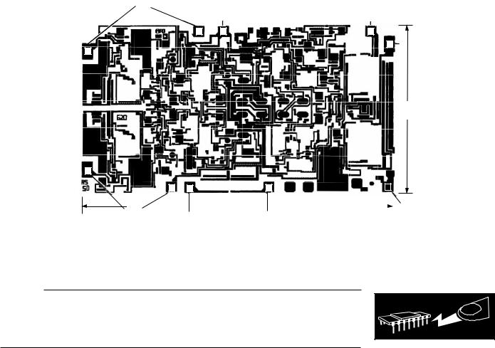
METALIZATION PHOTOGRAPH
Dimensions shown in inches and (mm).
Contact factory for latest dimensions.
RG* |
+VS |
OUTPUT |
|||||
|
|
|
|
|
|
|
|
|
|
|
|
|
|
|
|
8 |
7 |
|
6 |
|
|||
5 
 REFERENCE
8
0.0708
(1.799)
1
1 |
2 |
|
3 |
4 |
|
|
||
|
|
|
|
|
|
|
|
|
|
|
|
|
|
|
|
|
|
|
|
|
0.125 |
|
|
|
|
–V |
RG* |
|
|
(3.180) |
+IN |
|
|
|
S |
|
|
|
||||||
|
–IN |
|
|
|
|
|||
|
|
|
|
|
|
|||
*FOR CHIP APPLICATIONS: THE PADS 1RG AND 8RG MUST BE CONNECTED IN PARALLEL TO THE EXTERNAL GAIN REGISTER RG. DO NOT CONNECT THEM IN SERIES TO RG. FOR UNITY GAIN APPLICATIONS WHERE RG IS NOT REQUIRED, THE PADS 1RG MAY SIMPLY BE BONDED TOGETHER, AS WELL AS THE PADS 8RG.
CAUTION
ESD (electrostatic discharge) sensitive device. Electrostatic charges as high as 4000 V readily accumulate on the human body and test equipment and can discharge without detection. Although the AD620 features proprietary ESD protection circuitry, permanent damage may occur on devices subjected to high energy electrostatic discharges. Therefore, proper ESD precautions are recommended to avoid performance degradation or loss of functionality.
WARNING! |
ESD SENSITIVE DEVICE |
–4– |
REV. E |

AD620
Typical Characteristics (@ +258C, VS = 615 V, RL = 2 kV, unless otherwise noted)
PERCENTAGE OF UNITS
50
SAMPLE SIZE = 360
40
30
20
10
0 |
–80 |
–40 |
0 |
+40 |
+80 |
|
INPUT OFFSET VOLTAGE –mV |
|
||
INPUT BIAS CURRENT – nA
2.0
1.5
1.0
+IB
–I 0.5 B
0
–0.5
–1.0
–1.5
–2.0
–75 |
–25 |
25 |
75 |
125 |
175 |
|
TEMPERATURE –8C |
|
|
||
Figure 3. Typical Distribution of Input Offset Voltage |
Figure 6. Input Bias Current vs. Temperature |
50
SAMPLE SIZE = 850
|
40 |
|
|
|
|
UNITS |
30 |
|
|
|
|
OF |
|
|
|
|
|
|
|
|
|
|
|
PERCENTAGE |
20 |
|
|
|
|
10 |
|
|
|
|
|
|
|
|
|
|
|
|
0 |
|
|
|
|
|
–1200 |
–600 |
0 |
+600 |
+1200 |
|
|
INPUT BIAS CURRENT – pA |
|
||
Figure 4. Typical Distribution of Input Bias Current
|
50 |
|
|
|
|
|
SAMPLE SIZE = 850 |
|
|
|
|
|
40 |
|
|
|
|
UNITS |
30 |
|
|
|
|
OF |
|
|
|
|
|
|
|
|
|
|
|
PERCENTAGE |
20 |
|
|
|
|
|
10 |
|
|
|
|
|
0 |
–200 |
0 |
+200 |
+400 |
|
–400 |
||||
|
|
INPUT OFFSET CURRENT – pA |
|
||
Figure 5. Typical Distribution of Input Offset Current
|
2 |
|
–mV |
1.5 |
|
VOLTAGE |
||
|
||
OFFSETIN |
1 |
|
|
||
CHANGE |
0.5 |
|
|
||
|
0 |
0 |
1 |
2 |
3 |
4 |
5 |
WARM-UP TIME – Minutes
Figure 7. Change in Input Offset Voltage vs. Warm-Up Time
1000 |
|
|
|
|
|
|
|
|
|
GAIN = 1 |
|
|
|
nV/!Hz |
100 |
|
|
|
|
|
|
|
|
|
|
|
|
– |
|
|
GAIN = 10 |
|
|
|
NOISE |
|
|
|
|
|
|
|
|
|
|
|
|
|
VOLTAGE |
10 |
|
|
|
|
|
|
GAIN = 100, 1,000 |
|
|
|
||
|
|
|
|
|
||
|
|
|
|
GAIN = 1000 |
|
|
|
|
|
|
BW LIMIT |
|
|
|
1 |
10 |
|
|
|
|
|
1 |
100 |
1k |
10k |
100k |
|
|
|
|
FREQUENCY – Hz |
|
|
|
Figure 8. Voltage Noise Spectral Density vs. Frequency, (G = 1–1000)
REV. E |
–5– |
 Loading...