


Analog Devices AMP01NBS, AMP01GS-REEL, AMP01GS, AMP01GBC, AMP01FX Datasheet
...a |
Low Noise, Precision |
Instrumentation Amplifier |
FEATURES
Low Offset Voltage: 50 mV Max
Very Low Offset Voltage Drift: 0.3 mV/8C Max Low Noise: 0.12 mV p-p (0.1 Hz to 10 Hz) Excellent Output Drive: 610 V at 650 mA Capacitive Load Stability: to 1 mF
Gain Range: 0.1 to 10,000
Excellent Linearity: 16-Bit at G = 1000 High CMR: 125 dB min (G = 1000) Low Bias Current: 4 nA Max
May Be Configured as a Precision Op Amp Output-Stage Thermal Shutdown Available in Die Form
GENERAL DESCRIPTION
The AMP01 is a monolithic instrumentation amplifier designed for high-precision data acquisition and instrumentation applications. The design combines the conventional features of an instrumentation amplifier with a high current output stage. The output remains stable with high capacitance loads (1 µF), a unique ability for an instrumentation amplifier. Consequently, the AMP01 can amplify low level signals for transmission through long cables without requiring an output buffer. The output stage may be configured as a voltage or current generator.
Input offset voltage is very low (20 µV), which generally eliminates the external null potentiometer. Temperature changes have minimal effect on offset; TCVIOS is typically 0.15 µV/°C. Excellent low-frequency noise performance is achieved with a minimal compromise on input protection. Bias current is very low, less than 10 nA over the military temperature range. High common-mode rejection of 130 dB, 16-bit linearity at a gain of 1000, and 50 mA peak output current are achievable simultaneously. This combination takes the instrumentation amplifier one step further towards the ideal amplifier.
AC performance complements the superb dc specifications. The AMP01 slews at 4.5 V/µs into capacitive loads of up to 15 nF, settles in 50 µs to 0.01% at a gain of 1000, and boasts a healthy 26 MHz gain-bandwidth product. These features make the AMP01 ideal for high speed data acquisition systems.
Gain is set by the ratio of two external resistors over a range of 0.1 to 10,000. A very low gain temperature coefficient of 10 ppm/°C is achievable over the whole gain range. Output voltage swing is guaranteed with three load resistances; 50 Ω, 500 Ω, and 2 kΩ. Loaded with 500 Ω, the output delivers
± 13.0 V minimum. A thermal shutdown circuit prevents destruction of the output transistors during overload conditions.
The AMP01 can also be configured as a high performance operational amplifier. In many applications, the AMP01 can be used in place of op amp/power-buffer combinations.
REV. D
Information furnished by Analog Devices is believed to be accurate and reliable. However, no responsibility is assumed by Analog Devices for its use, nor for any infringements of patents or other rights of third parties which may result from its use. No license is granted by implication or otherwise under any patent or patent rights of Analog Devices.
AMP01*
PIN CONFIGURATIONS
18-Lead Cerdip
RG |
1 |
18 |
+IN |
RG |
2 |
17 |
VIOS NULL |
–IN 3 |
16 |
VIOS NULL |
|
VOOS NULL |
4 |
15 |
RS |
VOOS NULL |
5 |
14 |
RS |
TEST PIN* |
6 |
13 |
+VOP |
SENSE |
7 |
12 |
V+ |
REFERENCE |
8 |
11 |
V– |
OUTPUT |
9 |
10 |
–V |
|
|
AMP01 |
OP |
|
|
|
|
TOP VIEW (Not to Scale)
*MAKE NO ELECTRICAL CONNECTION
AMP01 BTC/883
28-Terminal LCC
|
|
|
|
|
|
|
|
|
|
|
|
NULL |
|
|
|
|
–IN |
G |
G |
|
NC |
+IN |
NC |
IOS |
|||
|
|
|
R |
R |
|
V |
|||||||
|
|
4 |
3 |
2 |
1 |
|
28 |
27 |
26 |
|
|||
NC 5 |
|
|
|
|
|
|
|
|
|
|
|
25 VIOS NULL |
|
|
|
|
|
|
|
|
|
|
|
|
|||
|
|
|
|
|
|
|
|
|
|
|
|||
VOOS NULL 6 |
|
|
|
|
|
|
|
|
|
|
|
24 NC |
|
NC 7 |
|
|
|
AMP01 |
|
|
23 RS |
||||||
VOOS NULL |
8 |
|
|
|
TOP VIEW |
|
|
22 RS |
|||||
NC |
9 |
|
|
(Not to Scale) |
|
21 +VOP |
|||||||
TEST PIN* 10 |
|
|
|
|
|
|
|
|
|
|
|
20 NC |
|
NC 11 |
|
|
|
|
|
|
|
|
|
|
|
19 V+ |
|
|
|
|
|
|
|
|
|
|
|
|
|
|
|
|
|
12 |
13 |
14 |
15 |
|
16 |
17 |
18 |
|
|||
|
|
|
SENSE |
REF |
OUT |
|
NC |
–V |
NC |
V– |
|||
NC = NO CONNECT |
|
|
|
|
|
|
|
|
OP |
|
|
|
|
|
|
|
|
|
|
|
|
|
|
|
|
||
*MAKE NO ELECTRICAL CONNECTION |
|||||||||||||
|
|
|
20-Lead SOIC |
|
|
||||||||
|
RG |
|
|
|
|
|
|
|
|
|
|
RG |
|
|
|
|
|
|
|
|
|
|
|
|
|||
|
|
1 |
|
|
|
|
|
|
|
20 |
|||
TEST PIN* |
|
|
|
|
|
|
|
|
|
|
TEST PIN* |
||
|
2 |
|
|
|
|
|
|
|
19 |
||||
|
–IN |
|
|
|
|
|
|
|
|
|
+IN |
||
|
3 |
|
|
|
|
|
|
|
18 |
||||
VOOS NULL |
|
|
|
|
|
|
|
|
|
|
VIOS NULL |
||
|
4 |
|
|
|
|
|
|
|
17 |
||||
VOOS NULL |
|
|
AMP01 |
|
|
VIOS NULL |
|||||||
|
5 |
|
16 |
||||||||||
TEST PIN* |
|
|
TOP VIEW |
|
RS |
||||||||
|
6 |
15 |
|||||||||||
|
(Not to Scale) |
||||||||||||
SENSE |
|
|
|
RS |
|||||||||
|
7 |
|
|
|
|
|
|
|
14 |
||||
REFERENCE |
|
|
|
|
|
|
|
|
|
|
+VOP |
||
|
8 |
|
|
|
|
|
|
|
13 |
||||
OUTPUT |
|
|
|
|
|
|
|
|
|
|
V+ |
||
|
9 |
|
|
|
|
|
|
|
12 |
||||
|
–V |
|
|
|
|
|
|
|
|
|
|
V– |
|
|
|
10 |
|
|
|
|
|
|
|
11 |
|||
|
OP |
|
|
|
|
|
|
|
|
|
|
||
|
|
|
|
|
|
|
|
|
|
|
|
|
|
*MAKE NO ELECTRICAL CONNECTION
*Protected under U.S. Patent Numbers 4,471,321 and 4,503,381.
One Technology Way, P.O. Box 9106, Norwood, MA 02062-9106, U.S.A.
Tel: 781/329-4700 |
World Wide Web Site: http://www.analog.com |
Fax: 781/326-8703 |
© Analog Devices, Inc., 1999 |
AMP01–SPECIFICATIONS
ELECTRICAL CHARACTERISTICS (@ VS = 615 V, RS = 10 kV, RL = 2 kV, TA = +258C, unless otherwise noted)
|
|
|
|
AMP01A |
|
AMP01B |
|
|
||
Parameter |
Symbol |
Conditions |
|
Min |
Typ |
Max |
Min |
Typ |
Max |
Units |
|
|
|
|
|
|
|
|
|
|
|
OFFSET VOLTAGE |
|
TA = +25°C |
|
|
20 |
50 |
|
40 |
100 |
µV |
Input Offset Voltage |
VIOS |
|
|
|
||||||
|
|
–55°C ≤ TA |
≤ +125°C |
|
40 |
80 |
|
60 |
150 |
µV |
Input Offset Voltage Drift |
TCVIOS |
–55°C ≤ TA |
≤ +125°C |
|
0.15 |
0.3 |
|
0.3 |
1.0 |
µV/°C |
Output Offset Voltage |
VOOS |
TA = +25°C |
|
|
1 |
3 |
|
2 |
6 |
mV |
|
|
–55°C ≤ TA ≤ +125°C |
|
3 |
6 |
|
6 |
10 |
mV |
|
Output Offset Voltage Drift |
TCVOOS |
RG = ∞ |
|
|
|
|
|
|
|
|
|
|
–55°C ≤ TA ≤ +125°C |
|
20 |
50 |
|
50 |
120 |
µV/°C |
|
Offset Referred to Input |
PSR |
G = 1000 |
|
120 |
130 |
|
110 |
120 |
|
dB |
vs. Positive Supply |
|
G = 100 |
|
110 |
130 |
|
100 |
120 |
|
dB |
V+ = +5 V to +15 V |
|
G = 10 |
|
95 |
110 |
|
90 |
100 |
|
dB |
|
|
G = 1 |
|
75 |
90 |
|
70 |
80 |
|
dB |
|
|
–55°C ≤ TA ≤ +125°C |
|
|
|
|
|
|
|
|
|
|
G = 1000 |
|
120 |
130 |
|
110 |
120 |
|
dB |
|
|
G = 100 |
|
110 |
130 |
|
100 |
120 |
|
dB |
|
|
G = 10 |
|
95 |
110 |
|
90 |
100 |
|
dB |
|
|
G = 1 |
|
75 |
90 |
|
70 |
80 |
|
dB |
Offset Referred to Input |
PSR |
G = 1000 |
|
105 |
125 |
|
105 |
115 |
|
dB |
vs. Negative Supply |
|
G = 100 |
|
90 |
105 |
|
90 |
95 |
|
dB |
V– = –5 V to –15 V |
|
G = 10 |
|
70 |
85 |
|
70 |
75 |
|
dB |
|
|
G = 1 |
|
50 |
65 |
|
50 |
60 |
|
dB |
|
|
–55°C ≤ TA ≤ +125°C |
|
|
|
|
|
|
|
|
|
|
G = 1000 |
|
105 |
125 |
|
105 |
115 |
|
dB |
|
|
G = 100 |
|
90 |
105 |
|
90 |
95 |
|
dB |
|
|
G = 10 |
|
70 |
85 |
|
70 |
75 |
|
dB |
Input Offset Voltage Trim |
|
G = 1 |
|
50 |
85 |
|
50 |
60 |
|
dB |
|
VS = ± 4.5 V to ± 18 V1 |
|
± 6 |
|
|
± 6 |
|
mV |
||
Range |
|
|
|
|
|
|||||
Output Offset Voltage Trim |
|
VS = ± 4.5 V to ± 18 V1 |
|
± 100 |
|
|
± 100 |
|
|
|
Range |
|
|
|
|
|
mV |
||||
INPUT CURRENT |
|
TA = +25°C |
|
|
1 |
4 |
|
2 |
6 |
nA |
Input Bias Current |
IB |
≤ +125°C |
|
|
||||||
|
|
–55°C ≤ TA |
|
4 |
10 |
|
6 |
15 |
nA |
|
Input Bias Current Drift |
TCIB |
–55°C ≤ TA |
≤ +125°C |
|
40 |
|
|
50 |
|
pA/°C |
Input Offset Current |
IOS |
TA = +25°C |
≤ +125°C |
|
0.2 |
1.0 |
|
0.5 |
2.0 |
nA |
|
|
–55°C ≤ TA |
|
0.5 |
3.0 |
|
1.0 |
6.0 |
nA |
|
Input Offset Current Drift |
TCIOS |
–55°C ≤ TA |
≤ +125°C |
|
3 |
|
|
5 |
|
pA/°C |
INPUT |
|
Differential, G = 1000 |
|
1 |
|
|
1 |
|
GΩ |
|
Input Resistance |
RIN |
|
|
|
|
|||||
|
|
Differential, G ≤ 100 |
|
10 |
|
|
10 |
|
GΩ |
|
|
|
Common Mode, G = 1000 |
|
20 |
|
|
20 |
|
GΩ |
|
Input Voltage Range |
IVR |
TA = +25°C2 |
± 10.5 |
|
|
± 10.5 |
|
|
V |
|
|
|
–55°C ≤ TA ≤ +125°C |
± 10.0 |
|
|
± 10.0 |
|
|
V |
|
Common-Mode Rejection |
CMR |
VCM = ± 10 V, 1 kΩ |
|
|
|
|
|
|
|
|
|
|
Source Imbalance |
|
|
|
|
|
|
|
|
|
|
G = 1000 |
|
125 |
130 |
|
115 |
125 |
|
dB |
|
|
G = 100 |
|
120 |
130 |
|
110 |
125 |
|
dB |
|
|
G = 10 |
|
100 |
120 |
|
95 |
110 |
|
dB |
|
|
G = 1 |
|
85 |
100 |
|
75 |
90 |
|
dB |
|
|
–55°C ≤ TA ≤ +125°C |
|
|
|
|
|
|
|
|
|
|
G = 1000 |
|
120 |
125 |
|
110 |
120 |
|
dB |
|
|
G = 100 |
|
115 |
125 |
|
105 |
120 |
|
dB |
|
|
G = 10 |
|
95 |
115 |
|
90 |
105 |
|
dB |
|
|
G = 1 |
|
80 |
95 |
|
75 |
90 |
|
dB |
|
|
|
|
|
|
|
|
|
|
|
NOTES
1VIOS and VOOS nulling has minimal affect on TCVIOS and TCVOOS respectively. 2Refer to section on common-mode rejection.
Specifications subject to change without notice.
–2– |
REV. D |
|
|
|
|
|
|
|
|
|
|
AMP01 |
||
|
|
(@ VS = 615 V, RS = 10 kV, RL = 2 kV, TA = +258C, –258C ≤ TA ≤ +858C for E, F |
|
|
|
|||||||
ELECTRICAL CHARACTERISTICS grades, 08C ≤ TA ≤ +708C for G grade, unless otherwise noted) |
|
|
|
|
|
|||||||
|
|
|
|
AMP01E |
|
AMP01F/G |
|
|
|
|
||
Parameter |
Symbol |
Conditions |
Min |
Typ |
Max |
Min |
Typ |
Max |
|
Units |
|
|
OFFSET VOLTAGE |
|
TA = +25°C |
|
20 |
50 |
|
40 |
100 |
|
µV |
||
Input Offset Voltage |
VIOS |
|
|
|
||||||||
|
|
TMIN ≤ TA ≤ TMAX |
|
40 |
80 |
|
60 |
150 |
|
µV |
||
Input Offset Voltage Drift |
TCVIOS |
|
1 |
|
0.15 |
0.3 |
|
0.3 |
1.0 |
|
µV/°C |
|
TMIN ≤ TA ≤ TMAX |
|
|
|
|||||||||
Output Offset Voltage |
VOOS |
TA = +25°C |
|
1 |
3 |
|
2 |
6 |
|
mV |
||
|
|
TMIN ≤ TA ≤ TMAX |
|
3 |
6 |
|
6 |
10 |
|
mV |
||
Output Offset Voltage Drift |
TCVOOS |
RG = ∞1 |
|
|
|
|
|
|
|
|
|
|
|
|
TMIN ≤ TA ≤ TMAX |
|
20 |
100 |
|
50 |
120 |
|
µV/°C |
||
Offset Referred to Input |
PSR |
G = 1000 |
|
120 |
130 |
|
110 |
120 |
|
|
dB |
|
vs. Positive Supply |
|
G = 100 |
|
110 |
130 |
|
100 |
120 |
|
|
dB |
|
V+ = +5 V to +15 V |
|
G = 10 |
|
95 |
110 |
|
90 |
100 |
|
|
dB |
|
|
|
G = 1 |
|
75 |
90 |
|
70 |
80 |
|
|
dB |
|
|
|
TMIN ≤ TA ≤ TMAX |
|
|
|
|
|
|
|
|
|
|
|
|
G = 1000 |
|
120 |
130 |
|
110 |
120 |
|
|
dB |
|
|
|
G = 100 |
|
110 |
130 |
|
100 |
120 |
|
|
dB |
|
|
|
G = 10 |
|
95 |
110 |
|
90 |
100 |
|
|
dB |
|
|
|
G = 1 |
|
75 |
90 |
|
70 |
80 |
|
|
dB |
|
Offset Referred to Input |
PSR |
G = 1000 |
|
110 |
125 |
|
105 |
115 |
|
|
dB |
|
vs. Negative Supply |
|
G = 100 |
|
95 |
105 |
|
90 |
95 |
|
|
dB |
|
V– = –5 V to –15 V |
|
G = 10 |
|
75 |
85 |
|
70 |
75 |
|
|
dB |
|
|
|
G = 1 |
|
55 |
65 |
|
50 |
60 |
|
|
dB |
|
|
|
TMIN ≤ TA ≤ TMAX |
|
|
|
|
|
|
|
|
|
|
|
|
G = 1000 |
|
110 |
125 |
|
105 |
115 |
|
|
dB |
|
|
|
G = 100 |
|
95 |
105 |
|
90 |
95 |
|
|
dB |
|
|
|
G = 10 |
|
75 |
85 |
|
70 |
75 |
|
|
dB |
|
Input Offset Voltage Trim |
|
G = 1 |
|
55 |
85 |
|
50 |
60 |
|
|
dB |
|
|
VS = ± 4.5 V to ± 18 V2 |
|
± 6 |
|
|
± 6 |
|
|
mV |
|||
Range |
|
|
|
|
|
|
||||||
Output Offset Voltage Trim |
|
VS = ± 4.5 V to ± 18 V2 |
|
± 100 |
|
|
± 100 |
|
|
|
|
|
Range |
|
|
|
|
|
|
mV |
|
||||
INPUT CURRENT |
|
TA = +25°C |
|
1 |
4 |
|
2 |
6 |
|
mV |
||
Input Bias Current |
IB |
|
|
|
||||||||
|
|
TMIN ≤ TA |
≤ TMAX |
|
4 |
10 |
|
6 |
15 |
|
mV |
|
Input Bias Current Drift |
TCIB |
TMIN ≤ TA |
≤ TMAX |
|
40 |
|
|
50 |
|
|
pA/°C |
|
Input Offset Current |
IOS |
TA = +25°C |
|
0.2 |
1.0 |
|
0.5 |
2.0 |
|
mV |
||
|
|
TMIN ≤ TA |
≤ TMAX |
|
0.5 |
3.0 |
|
1.0 |
6.0 |
|
mV |
|
Input Offset Current Drift |
TCIOS |
TMIN ≤ TA |
≤ TMAX |
|
3 |
|
|
5 |
|
|
pA/°C |
|
INPUT |
|
Differential, G = 1000 |
|
1 |
|
|
1 |
|
|
GΩ |
||
Input Resistance |
RIN |
|
|
|
|
|
||||||
|
|
Differential, G ≤ 100 |
|
10 |
|
|
10 |
|
|
GΩ |
||
|
|
Common Mode, G = 1000 |
|
20 |
|
|
20 |
|
|
GΩ |
||
Input Voltage Range |
IVR |
TA = +25°C3 |
± 10.5 |
|
|
± 10.5 |
|
|
|
V |
||
|
|
TMIN ≤ TA ≤ TMAX |
± 10.0 |
|
|
± 10.0 |
|
|
|
V |
||
Common-Mode Rejection |
CMR |
VCM = ± 10 V, 1 kΩ |
|
|
|
|
|
|
|
|
|
|
|
|
Source Imbalance |
|
|
|
|
|
|
|
|
|
|
|
|
G = 1000 |
|
125 |
130 |
|
115 |
125 |
|
|
dB |
|
|
|
G = 100 |
|
120 |
130 |
|
110 |
125 |
|
|
dB |
|
|
|
G = 10 |
|
100 |
120 |
|
95 |
110 |
|
|
dB |
|
|
|
G = 1 |
|
85 |
100 |
|
75 |
90 |
|
|
dB |
|
|
|
TMIN ≤ TA ≤ TMAX |
|
|
|
|
|
|
|
|
|
|
|
|
G = 1000 |
|
120 |
125 |
|
110 |
120 |
|
|
dB |
|
|
|
G = 100 |
|
115 |
125 |
|
105 |
120 |
|
|
dB |
|
|
|
G = 10 |
|
95 |
115 |
|
90 |
105 |
|
|
dB |
|
|
|
G = 1 |
|
80 |
95 |
|
75 |
90 |
|
|
dB |
|
NOTES 1Sample tested.
2VIOS and VOOS nulling has minimal affect on TCVIOS and TCVOOS, respectively. 3Refer to section on common-mode rejection.
Specifications subject to change without notice.
REV. D |
–3– |
AMP01
ELECTRICAL CHARACTERISTICS
(@ VS = 615 V, RS = 10 kV, RL = 2 kV, TA = +258C, unless otherwise noted)
|
|
|
|
|
|
|
AMP01A/E |
AMP01B/F/G |
|
|||
Parameter |
Symbol |
Conditions |
Min |
Typ |
Max |
Min |
Typ |
Max |
Units |
|||
|
|
|
|
|
|
|
|
|
|
|
|
|
GAIN |
|
|
|
|
|
|
|
|
|
|
|
|
|
|
20 × RS |
|
|
|
|
|
|
|
|||
Gain Equation Accuracy |
|
G = |
|
|
|
|
0.3 |
0.6 |
|
0.5 |
0.8 |
% |
|
|
RG |
|
|
||||||||
|
|
|
|
|
|
|
|
|
|
|
||
|
|
Accuracy Measured |
|
|
|
|
|
|
|
|||
Gain Range |
G |
from G = 1 to 1000 |
0.1 |
|
10k |
0.1 |
|
10k |
V/V |
|||
G = 10001 |
|
|
||||||||||
Nonlinearity |
|
|
0.0007 0.005 |
|
0.0007 0.005 |
% |
||||||
|
|
G = 1001 |
|
|
0.005 |
|
|
0.005 |
% |
|||
|
|
G = 101 |
|
|
0.005 |
|
|
0.007 |
% |
|||
|
|
G = 11 |
|
|
|
|
0.010 |
|
|
0.015 |
% |
|
Temperature Coefficient |
GTC |
1 ≤ G ≤ 10001, 2 |
|
5 |
10 |
|
5 |
15 |
ppm°C |
|||
OUTPUT RATING |
|
RL = 2 kΩ |
± 13.0 |
± 13.8 |
|
± 13.0 |
± 13.8 |
|
V |
|||
Output Voltage Swing |
VOUT |
|
|
|||||||||
|
|
RL = 500 Ω |
± 13.0 |
± 13.5 |
|
± 13.0 |
± 13.5 |
|
V |
|||
|
|
RL = 50 Ω |
± 2.5 |
± 4.0 |
|
± 2.5 |
± 4.0 |
|
V |
|||
|
|
RL = 2 kΩ Over Temp. |
± 12.0 |
± 13.8 |
|
± 12.0 |
± 13.8 |
|
V |
|||
|
|
RL = 500 Ω3 |
± 12.0 |
± 13.5 |
|
± 12.0 |
± 13.5 |
|
V |
|||
Positive Current Limit |
|
Output-to-Ground Short |
60 |
100 |
120 |
60 |
100 |
120 |
mA |
|||
Negative Current Limit |
|
Output-to-Ground Short |
60 |
90 |
120 |
60 |
90 |
120 |
mA |
|||
Capacitive Load Stability |
|
1 ≤ G ≤ 1000 |
|
|
|
|
|
|
µF |
|||
Thermal Shutdown |
|
No Oscillations1 |
0.1 |
1 |
|
0.1 |
1 |
|
||||
|
|
|
|
|
|
|
|
|
|
|
°C |
|
Temperature |
|
Junction Temperature |
|
165 |
|
|
165 |
|
||||
|
|
|
|
|
|
|
|
|
|
|
|
|
NOISE |
|
fO = 1 kHz |
|
|
|
|
|
|
|
|||
Voltage Density, RTI |
en |
|
|
|
|
|
|
nV/√Hz |
||||
|
en |
G = 1000 |
|
5 |
|
|
5 |
|
||||
|
en |
G = 100 |
|
10 |
|
|
10 |
|
nV/√Hz |
|||
|
en |
G = 10 |
|
|
|
59 |
|
|
59 |
|
nV/√Hz |
|
|
en |
G = 1 |
|
|
|
540 |
|
|
540 |
|
nV/√Hz |
|
Noise Current Density, RTI |
in |
fO = 1 kHz, G = 1000 |
|
0.15 |
|
|
0.15 |
|
pA/√Hz |
|||
Input Noise Voltage |
en p-p |
0.1 Hz to 10 Hz |
|
|
|
|
|
|
µV p-p |
|||
|
en p-p |
G = 1000 |
|
0.12 |
|
|
0.12 |
|
||||
|
en p-p |
G = 100 |
|
0.16 |
|
|
0.16 |
|
µV p-p |
|||
|
en p-p |
G = 10 |
|
|
|
1.4 |
|
|
1.4 |
|
µV p-p |
|
|
en p-p |
G = 1 |
|
|
|
13 |
|
|
13 |
|
µV p-p |
|
Input Noise Current |
in p-p |
0.1 Hz to 10 Hz, G = 1000 |
|
2 |
|
|
2 |
|
pA p-p |
|||
DYNAMIC RESPONSE |
|
|
|
|
|
|
|
|
|
|
|
|
Small-Signal |
|
G = 1 |
|
|
|
570 |
|
|
570 |
|
kHz |
|
Bandwidth (–3 dB) |
BW |
G = 10 |
|
|
|
100 |
|
|
100 |
|
kHz |
|
|
|
G = 100 |
|
82 |
|
|
82 |
|
kHz |
|||
|
|
G = 1000 |
|
26 |
|
|
26 |
|
kHz |
|||
Slew Rate |
SR |
G = 10 |
|
|
3.5 |
4.5 |
|
3.0 |
4.5 |
|
V/µs |
|
Settling Time |
tS |
To 0.01%, 20 V step |
|
|
|
|
|
|
µs |
|||
|
|
G = 1 |
|
|
|
12 |
|
|
12 |
|
||
|
|
G = 10 |
|
|
|
13 |
|
|
13 |
|
µs |
|
|
|
G = 100 |
|
15 |
|
|
15 |
|
µs |
|||
|
|
G = 1000 |
|
50 |
|
|
50 |
|
µs |
|||
|
|
|
|
|
|
|
|
|
|
|
|
|
NOTES
1Guaranteed by design.
2Gain tempco does not include the effects of gain and scale resistor tempco match.
3–55°C ≤ TA ≤ +125°C for A/B grades, –25°C ≤ TA ≤ +85°C for E/F grades, 0°C ≤ TA ≤ 70°C for G grades. Specifications subject to change without notice.
–4– |
REV. D |

ELECTRICAL CHARACTERISTICS (@ VS = 615 V, RS = 10 kV, RL = 2 kV, TA = +258C, unless otherwise noted) |
AMP01 |
|||||||||||||||
|
||||||||||||||||
|
|
|
|
|
|
|
|
|
|
|
|
|||||
|
|
|
|
|
|
|
AMP01A/E |
|
AMP01B/F/G |
|
||||||
Parameter |
|
Symbol |
Conditions |
|
Min |
Typ |
Max |
|
Min |
Typ |
Max |
Units |
||||
|
|
|
|
|
|
|
|
|
|
|
|
|
|
|
|
|
SENSE INPUT |
|
|
|
|
|
|
35 |
50 |
65 |
|
35 |
50 |
|
65 |
kΩ |
|
Input Resistance |
|
RIN |
|
|
|
|
|
|||||||||
Input Current |
|
IIN |
Referenced to V– |
|
|
280 |
|
|
|
|
280 |
|
µA |
|||
Voltage Range |
|
|
|
(Note 1) |
|
–10.5 |
|
+15 |
|
–10.5 |
|
|
+15 |
V |
||
|
|
|
|
|
|
|
|
|
|
|
|
|
|
|
|
|
REFERENCE INPUT |
|
|
|
|
|
|
35 |
50 |
65 |
|
35 |
50 |
|
65 |
kΩ |
|
Input Resistance |
|
RIN |
|
|
|
|
|
|||||||||
Input Current |
|
IIN |
Referenced to V– |
|
|
280 |
|
|
|
|
280 |
|
µA |
|||
Voltage Range |
|
|
|
(Note 1) |
|
–10.5 |
|
+15 |
|
–10.5 |
|
|
+15 |
V |
||
Gain to Output |
|
|
|
|
|
|
|
1 |
|
|
|
|
1 |
|
|
V/V |
|
|
|
|
|
|
|
|
|
|
|
|
|
|
|||
POWER SUPPLY –25°C ≤ TA ≤ +85°C for E/F Grades, –55°C ≤ TA ≤ +125°C for A/B Grades |
|
|
|
|
|
|
||||||||||
Supply Voltage Range |
|
VS |
|
+V linked to +VOP |
|
± 4.5 |
|
± 18 |
|
± 4.5 |
|
|
± 18 |
V |
||
|
|
|
|
|
|
|
||||||||||
|
|
VS |
|
–V linked to –VOP |
|
± 4.5 |
|
± 18 |
|
± 4.5 |
|
|
± 18 |
V |
||
Quiescent Current |
|
IQ |
|
+V linked to +VOP |
|
|
3.0 |
4.8 |
|
|
3.0 |
4.8 |
mA |
|||
|
|
IQ |
|
–V linked to –VOP |
|
|
3.4 |
4.8 |
|
|
3.4 |
4.8 |
mA |
|||
NOTE |
|
|
|
|
|
|
|
|
|
|
|
|
|
|
|
|
1Guaranteed by design. |
|
|
|
|
|
|
|
|
|
|
|
|
|
|
|
|
Specifications subject to change without notice. |
|
|
|
|
|
|
|
|
|
|
|
|
|
|||
|
|
|
|
|
ORDERING GUIDE |
|
|
|
|
|
|
|
|
|
||
|
|
|
|
|
|
|
|
|
|
|
|
|
||||
|
Model |
|
Temperature Range |
Package Description |
Package Option |
|
|
|||||||||
|
|
|
|
|
|
|
|
|
|
|
|
|
|
|
|
|
|
AMP01AX |
|
–55°C to +125°C |
18-Lead Cerdip |
|
Q-18 |
|
|
|
|
|
|||||
|
AMP01AX/883C |
|
–55°C to +125°C |
18-Lead Cerdip |
|
Q-18 |
|
|
|
|
|
|||||
|
AMP01BTC/883C |
|
–55°C to +125°C |
28-Terminal LCC |
|
E-28A |
|
|
|
|
|
|||||
|
AMP01BX |
|
–55°C to +125°C |
18-Lead Cerdip |
|
Q-18 |
|
|
|
|
|
|||||
|
AMP01BX/883C |
|
–55°C to +125°C |
18-Lead Cerdip |
|
Q-18 |
|
|
|
|
|
|||||
|
AMP01EX |
|
–25°C to +85°C |
18-Lead Cerdip |
|
Q-18 |
|
|
|
|
|
|||||
|
AMP01FX |
|
–25°C to +85°C |
18-Lead Cerdip |
|
Q-18 |
|
|
|
|
|
|||||
|
AMP01GBC |
|
0°C to +70°C |
Die |
|
|
|
|
|
|
|
|
|
|||
|
AMP01GS |
|
20-Lead SOIC |
|
R-20 |
|
|
|
|
|
||||||
|
AMP01GS-REEL |
|
0°C to +70°C |
13" Tape and Reel |
|
R-20 |
|
|
|
|
|
|||||
|
AMP01NBC |
|
–55°C to +125°C |
Die |
|
|
|
|
|
|
|
|
|
|||
|
5962-8863001VA* |
18-Lead Cerdip |
|
Q-18 |
|
|
|
|
|
|||||||
|
5962-88630023A* |
–55°C to +125°C |
28-Terminal LCC |
|
E-28A |
|
|
|
|
|||||||
|
5962-8863002VA* |
–55°C to +125°C |
18-Lead Cerdip |
|
Q-18 |
|
|
|
|
|
||||||
*Standard military drawing available.
DICE CHARACTERISTICS
Die Size 0.111 × 0.149 inch, 16,539 sq. mils (2.82 × 3.78 mm, 10.67 sq. mm)
1. |
RG |
10. |
V– (OUTPUT) |
|
2. |
RG |
11. |
V– |
|
3. |
–INPUT |
12. |
V+ |
|
13. |
V+ (OUTPUT) |
|||
4. |
VOOS NULL |
|||
14. |
RS |
|||
5. |
VOOS NULL |
|||
15. |
RS |
|||
6. |
TEST PIN* |
|||
16. |
VIOS NULL |
|||
7. |
SENSE |
|||
8. |
REFERENCE |
17. |
VIOS NULL |
|
9. |
OUTPUT |
18. |
+INPUT |
* MAKE NO ELECTRICAL CONNECTION
REV. D |
–5– |
AMP01
WAFER TEST LIMITS
(@ VS = 615 V, RS = 10 kV, RL = 2 kV, TA = +258C, unless otherwise noted)
|
|
|
|
|
|
AMP01NBC |
AMP01GBC |
|
Parameter |
Symbol |
Conditions |
Limit |
Limit |
Units |
|||
|
|
|
|
|
|
|
|
|
Input Offset Voltage |
VIOS |
|
|
|
|
60 |
120 |
µV max |
Output Offset Voltage |
VOOS |
|
|
|
|
4 |
8 |
mV max |
Offset Referred to Input |
PSR |
V+ = +5 V to +15 V |
|
|
dB min |
|||
vs. Positive Supply |
|
G = 1000 |
120 |
110 |
dB min |
|||
|
|
G = 100 |
110 |
100 |
dB min |
|||
|
|
G = 10 |
|
|
95 |
90 |
dB min |
|
|
|
G = 1 |
|
|
75 |
70 |
dB min |
|
Offset Referred to Input |
PSR |
V– = –5 V to –15 V |
|
|
dB min |
|||
vs. Negative Supply |
|
G = 1000 |
105 |
105 |
dB min |
|||
|
|
G = 100 |
90 |
90 |
dB min |
|||
|
|
G = 10 |
|
|
70 |
70 |
dB min |
|
|
|
G = 1 |
|
|
50 |
50 |
dB min |
|
Input Bias Current |
IB |
|
|
|
|
4 |
8 |
nA max |
Input Offset Current |
IOS |
|
|
|
|
1 |
3 |
nA max |
Input Voltage Range |
IVR |
Guaranteed by CMR Tests |
± 10 |
± 10 |
V min |
|||
Common Mode Rejection |
CMR |
VCM = ± 10 V |
|
|
dB min |
|||
|
|
G = 1000 |
125 |
115 |
dB min |
|||
|
|
G = 100 |
120 |
110 |
dB min |
|||
|
|
G = 10 |
|
|
100 |
95 |
dB min |
|
|
|
G = 1 |
|
|
85 |
75 |
dB min |
|
Gain Equation Accuracy |
|
G = |
20 × RS |
|
0.6 |
0.8 |
% max |
|
|
|
RG |
||||||
|
|
|
|
|
|
|
||
Output Voltage Swing |
VOUT |
RL = 2 kΩ |
± 13 |
± 13 |
V min |
|||
|
VOUT |
RL = 500 Ω |
± 13 |
± 13 |
V min |
|||
|
VOUT |
RL = 50 Ω |
± 2.5 |
± 2.5 |
V min |
|||
Output Current Limit |
|
Output to Ground Short |
± 60 |
± 60 |
mA min |
|||
Output Current Limit |
|
Output to Ground Short |
± 120 |
± 120 |
mA max |
|||
Quiescent Current |
IQ |
+V Linked to +VOP |
4.8 |
4.8 |
mA max |
|||
|
|
–V Linked to –VOP |
4.8 |
4.8 |
mA max |
|||
NOTE
Electrical tests are performed at wafer probe to the limits shown. Due to variations in assembly methods and normal yield loss, yield after packaging is not guaranteed for standard product dice. Consult factory to negotiate specifications based on dice lot qualification through sample lot assembly and testing.
|
|
|
V+ |
|
VIOS |
|
+VOP |
|
NULL |
|
|
|
|
A1 |
OUTPUT |
250V |
|
|
–V |
–IN |
|
|
|
|
|
OP |
|
250V |
|
|
|
+IN |
Q1 |
Q2 |
|
REFERENCE |
|
|
|
R1 |
|
|
|
47.5kV |
RGAIN |
|
R3 |
|
|
47.5kV |
|
|
|
|
SENSE |
A2 |
|
A3 |
|
|
RSCALE |
|
|
R2 |
VOOS |
|
R4 |
2.5kV |
NULL |
|
2.5kV |
|
|
|
|
|
|
|
V– |
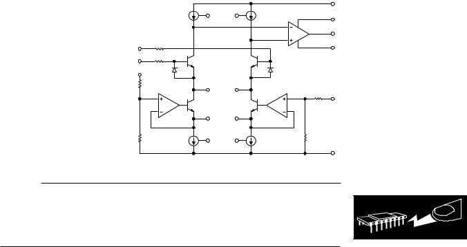
Figure 1. Simplified Schematic
CAUTION
ESD (electrostatic discharge) sensitive device. Electrostatic charges as high as 4000 V readily accumulate on the human body and test equipment and can discharge without detection. Although the AMP01 features proprietary ESD protection circuitry, permanent damage may occur on devices subjected to high energy electrostatic discharges. Therefore, proper ESD precautions are recommended to avoid performance degradation or loss of functionality.
WARNING! |
ESD SENSITIVE DEVICE |
–6– |
REV. D |
|
|
|
|
|
AMP01 |
|
ELECTRICAL CHARACTERISTICS (@ VS = 615 V, RS = 10 kV, RL = 2 kV, TA = +258C, unless otherwise noted) |
|
|
||||
|
|
|
|
|
|
|
|
|
|
AMP01NBC |
AMP01GBC |
|
|
Parameter |
Symbol |
Conditions |
Typical |
Typical |
Units |
|
|
|
|
|
|
|
|
Input Offset Voltage Drift |
TCVIOS |
RG = ∞ |
0.15 |
0.30 |
V/°C |
|
Output Offset Voltage Drift |
TCVOOS |
20 |
50 |
V/°C |
||
Input Bias Current Drift |
TCIB |
|
40 |
50 |
pA/°C |
|
Input Offset Current Drift |
TCIOS |
|
3 |
5 |
pA/°C |
|
Nonlinearity |
|
G = 1000 |
0.0007 |
0.0007 |
% |
|
Voltage Noise Density |
en |
G = 1000 |
|
|
nV/√Hz |
|
|
in |
fO = 1 kHz |
5 |
5 |
||
Current Noise Density |
G = 1000 |
|
|
pA/√Hz |
||
|
en p-p |
fO = 1 kHz |
0.15 |
0.15 |
||
Voltage Noise |
G = 1000 |
|
|
V p-p |
||
|
|
0.1 Hz to 10 Hz |
0.12 |
0.12 |
||
Current Noise |
in p-p |
G = 1000 |
2 |
2 |
pA p-p |
|
|
|
0.1 Hz to 10 Hz |
|
|
|
|
Small-Signal Bandwidth (–3 dB) |
BW |
G = 1000 |
26 |
26 |
kHz |
|
Slew Rate |
SR |
G = 10 |
4.5 |
4.5 |
V/ s |
|
Settling Time |
tS |
To 0.01%, 20 V Step |
|
|
s |
|
|
|
G = 1000 |
50 |
50 |
||
|
|
|
|
|
|
|
NOTE
Electrical tests are performed at wafer probe to the limits shown. Due to variations in assembly methods and normal yield loss, yield after packaging is not guaranteed for standard product dice. Consult factory to negotiate specifications based on dice lot qualification through sample lot assembly and testing.
REV. D |
–7– |
 Loading...