


AME8816CEHAADJ
Analog Microelectronics AME8816CEHAADJ, AME8816BEHAADJ, AME8816BEDVADJ, AME8816AEHA500, AME8816AEHA475 Datasheet
...
AME, Inc.
AME8816
nn
n General Description
nn
The AME8816 family of positive, linear regulators feature low quiescent current (45µA typ.) with low dropout
voltage, making them ideal for battery applications.
Output voltages are set at the factory and trimmed to
1.5% accuracy.
These rugged devices have both Thermal Shutdown,
and Current Fold-back to prevent device failure under
the "Worst" of operating conditions.
In applications requiring a low noise, regulated supply,
place a 1000pF capacitor between Bypass and Ground.
The AME8816 is stable with an output capacitance of
4.7µF or greater .
nn
n Features
nn
1.5A CMOS LDO
nn
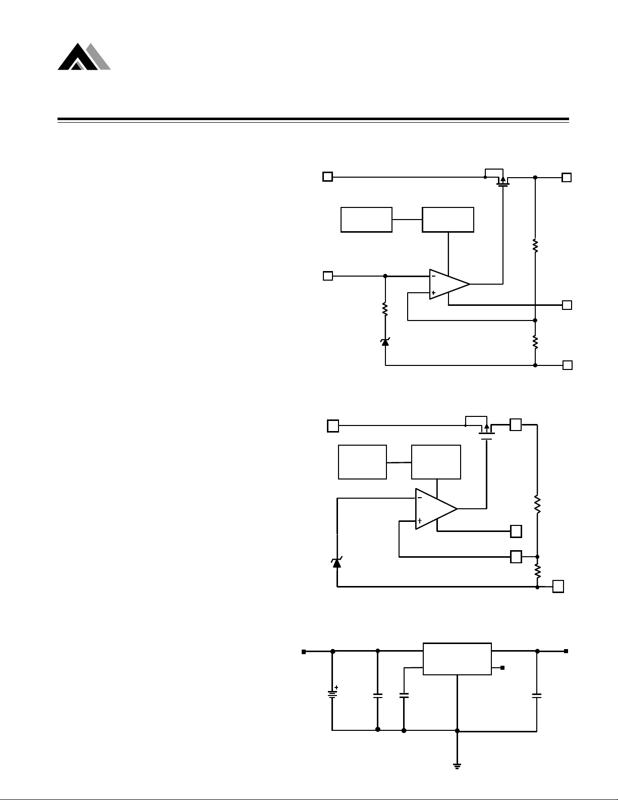
nFunctional Block Diagram
nn
(Fixed Versions)
Overcurrent
Shutdown
BYPASS
1.242V
nn
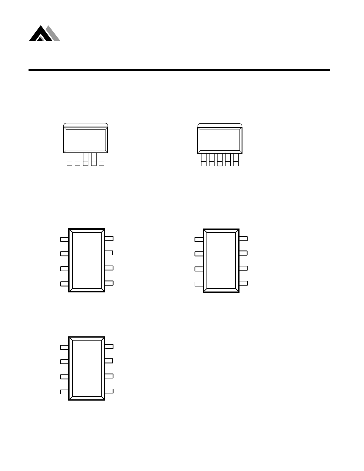
nFunctional Block Diagram
nn
Thermal
Shutdown
AMP
OUTIN
R1
EN
R2
GND
l Very Low Dropout Voltage
l Guaranteed 1.5A Output
l Accurate to within 1.5%
l 45µA Quiescent Current Typically
l Over-Temperature Shutdown
l Current Limiting
l Short Circuit Current Fold-back
l Noise Reduction Bypass Capacitor (Fixed
Versions)
l Power-Saving Shutdown Mode
l Space-Saving DDPAK-5 Package
l 6 Factory Pre-set Output Voltages
l Low Temperature Coef ficient
l Adjustable Version
nn
n Applications
nn
l Instrumentation
l Portable Electronics
l Wireless Devices
l PC Peripherals
l Battery Powered Widgets
(Adjustable Version)
IN
Overcurrent
Shutdown
1.242V
nn
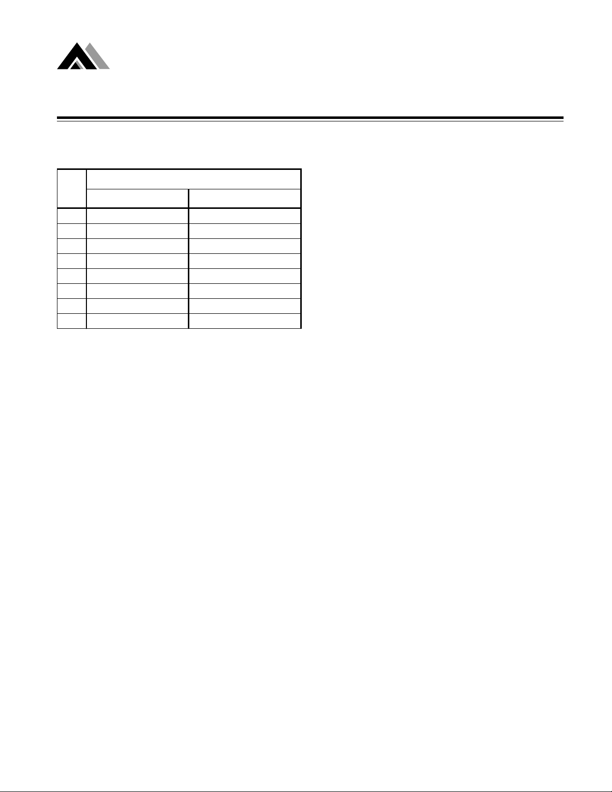
n T ypical Application
nn
IN
C1
5V
1µF
C2
1nF
Thermal
Shutdown
AMP
IN
BYP
AME8816
OUT
GND
EN
OUT
EN
ADJ
R1
(external)
R2
(external)
GND
OUT
C3
4.7µ
F
1
AME, Inc.
AME8816
nn
n Pin Configuration
nn
AME8816
AEDVXXX
YYWW
12345
TO-263(DDPAK-5) Top View
1. EN
2. V
IN
3. GND
4. V
OUT
5. BYP
AME8816
BEDV ADJ
YYWW
12345
SO-8 Top View
1.5A CMOS LDO
1. EN
2. V
IN
3. GND
4. V
OUT
5. ADJ
8
7
6
5
1. ADJ
2. GND
3. GND
4. EN
5. V
IN
6. GND
7. GND
8. V
OUT
1
O
8
2. GND
1
O
3. GND
1. BYP
2
8816
AEHAXXX
3
4
YYWW
7
6
4. EN
5. V
IN
6. GND
5
7. GND
8. V
OUT
2
3
4
8816
BEHAADJ
YYWW
1. EN
1
2
O
8816
CEHAADJ
3
4
YYWW
8
2. V
IN
3. V
7
6
OUT
4. ADJ
5. GND
6. GND
7. GND
5
8. GND
2
AME, Inc.
AME8816
nnnn
AME8816 Ordering Information
1.5A CMOS LDO
Package Type
V
OUT
DDPAK-5 SO-8
1.50 AM E 8816A EDV150 AM E 8816A EHA150
1.80 AM E 8816A EDV180 AM E 8816A EHA180
2.50 AM E 8816A EDV250 AM E 8816A EHA250
3.30 AM E 8816A EDV330 AM E 8816A EHA330
4.75 AM E 8816A EDV475 AM E 8816A EHA475
5.00 AM E 8816A EDV500 AM E 8816A EHA500
ADJ AME8816B EDVA DJ AM E 8816B EHAA DJ
ADJ AM E 8816CE HA A DJ
Please c ons ult A ME sal es office or authorized Rep./ Distr. F or ot her out put voltage and pack age t ype or pinout
availabili t y.
3
AME, Inc.
AME8816
Absolute Maximum Ratings:
nnnn
Parameter Maximum Unit
Inpu t Vo l ta ge 8 V
Output Current
Output V olt age GND - 0.3 to V
ESD Class i fic at i on B
Caution: S t res s above the lis t ed abs olut e m aximum rati ng may c aus e permanent damage t o t he device.
Recommended operating Conditions:
nnnn
Parameter Rating Un it
Am bient Temperature Range -40 to +85
PD / (VIN - VO)
+ 0.3 V
IN
1.5A CMOS LDO
mA
o
C
Junction Temperature -40 to +125
Thermal Information
nnnn
Parame ter
TO-263 (DDPAK -5) 5
Thermal Resistance (
Internal Power Diss ipat ion (P
o
(∆T = 100
Max im um Junct i on Temperature
Max im um Lead Temperature ( 10 Sec)
C)*
)
θ
jc
)
D
SO-8 20**
TO-263 (DDPAK -5) 3.00
SO-8 2.50
o
C
Maximum Unit
o
C / W
W
150
300
o
C
o
C
* As s um ing a heat s ink c apable of twice t imes (
** Estimated
4
)
θ
jc
AME, Inc.
AME8816
nn
n Electrical Specifications
nn
V
= V
IN
Input Voltage V
Output Voltage Accuracy V
Dropout Voltage V
Output C urrent I
Current Limit I
Short Circuit Current I
Quiescent Current I
M inimun Load Current
(For ADJ Option)
Ground Pin Current I
Line Regulation RE G
Load Regulation RE G
+2V, VEN = VIN, TA = 25oC unless otherwise noted
O(nom)
Para mete r Symb ol Min Typ Ma x Units
IN
O
DROPOUT
O
LIM
SC
Q
I
MIN
GND
LINE
LOAD
IO=1.5A
V
O=VONOM
IO=1mA
V
IN=VO
Te st Condition
V
= VEHmin, IO=1mA
EN
-2.0%
V
O
V
O
V
O
I
O
=1m A to 1.5A
I
O
+1 to VO+2
I
=1m A to 1.5A
O
1.5V < V
2.0V <V
>1.2V
>1.2V
<0.4V
=0mA
Note 1 7 V
-1.5 1. 5 %
<= 2.0V 1300
O(NOM)
<= 2.8V 800
O(NOM)
2.8V <V
O(NOM)
1500 m A
1500 2000 m A
< 2.0V -0.15 0.15 %
V
O
4.0 > V
>= 2.0V -0.1 0.02 0.1 %
O
4.0V <= V
O
-0.4 0. 4 %
1.5A CMOS LDO
See
chart
750 m A
1mA
-1 0. 2 1 %
Over Temerature Shut down OTS 150
Over Temerature Hys terisis OTH 30
Temperature Coefficient TC 30
V
O
AD J Input Bias C urrent I
AD J Reference V oltage V
ADJ
REF
V
= 5V , V
IN
= 1.24 2V
ADJ
1.223 1.242 1.261 V
f=1kHz 50
I
=100mA
Pow er Supply Rejec tion
Pow er Supply Rejec tion
PS RR f=10kHz 20 dB
PS RR f=10kHz 55 dB
Output V oltage Nois e eN
O
=4.7µF ceramic
C
O
I
=100mA
O
=4.7µF ceramic
C
O
=0.01µF
C
BY P
f=10Hz t o 100k Hz
I
=10mA ,C
O
BY P
=0µF
f=100kHz 15
f=1kHz 75
f=100kHz 30
Co=4.7µF30
600
45 70
45
1
mV
µ
µ
o
o
ppm /
µ
Vrms
µ
A
A
C
C
o
C
A
Output V oltage Nois e eN
EN Input Threshold
EN Input Bias Current
Shut down S upply Current I
Note1.V
Note2.V
IN(min)=VOUT+VDROPOUT
O(nom) :
nom inal output voltage of fixed version
V
V
I
EH
I
EL
SD
EH
EL
f=10Hz t o 100k Hz
I
=10mA ,C
O
BY P
=0.01µF
V
V
= 5V , VO=0V, VEN=0V
IN
VIN= 7V
=0V, VIN= 7V
EN
Co=4.7µF30
Vrms
µ
2.0 Vin V
00.4V
0.1
0.5
0.5 2
A
µ
A
µ
A
µ
5
 Loading...