


MACH110-12

Publication# 14127 Rev. I Amendment/0
Issue Date: May 1995
Advanced
Micro
Devices
MACH110-12/15/20
High-Density EE CMOS Programmable Logic
FINAL
COM’L: -12/15/20 IND: -14/18/24
DISTINCTIVE CHARACTERISTICS
■ 44 Pins
■ 32 Macrocells
■ 12 ns t
PD
Commercial
14 ns t
PD
Industrial
■ 77 MHz f
CNT
■ 38 Inputs
■ 32 Outputs
■ 32 Flip-flops; 2 clock choices
■ 2 “PAL22V16” Blocks
■ Pin-compatible with MACH111, MACH210,
MACH211, MACH215
GENERAL DESCRIPTION
The MACH110 is a member of AMD’s high-performance
EE CMOS MACH 1 family. This device has approxi-
mately three times the logic macrocell capability of the
popular PAL22V10 without loss of speed.
The MACH110 consists of two PAL blocks intercon-
nected by a programmable switch matrix. The two PAL
blocks are essentially “PAL22V16” structures complete
with product-term arrays and programmable macro-
cells. The switch matrix connects the PAL blocks to
each other and to all input pins, providing a high degree
of connectivity between the fully-connected PAL blocks.
This allows designs to be placed and routed efficiently.
The MACH110 macrocell provides either registered or
combinatorial outputs with programmable polarity. If a
registered configuration is chosen, the register can be
configured as D-type or T-type to help reduce the
number of product terms. The register type decision can
be made by the designer or by the software. All
macrocells can be connected to an I/O cell. If a buried
macrocell is desired, the internal feedback path from the
macrocell can be used, which frees up the I/O pin for use
as an input.
查询MACH110-14供应商
AMD
2 MACH110-12/15/20
BLOCK DIAGRAM
44 x 70
AND Logic Array
and
Logic Allocator
44 x 70
AND Logic Array
and
Logic Allocator
I/O
0
– I/O
15
I
0
– I
1,
I
3
– I
4
I/O
Cells
Macrocells
Switch Matrix
Macrocells
I/O
Cells
I/O
16
– I/O
31
CLK
1
/I
5,
CLK
0
/I
2
14127I-1
16
16
16
16
22
22
16
16
16
16
2
4
2
2
2
OE
OE
AMD
3MACH110-12/15/20
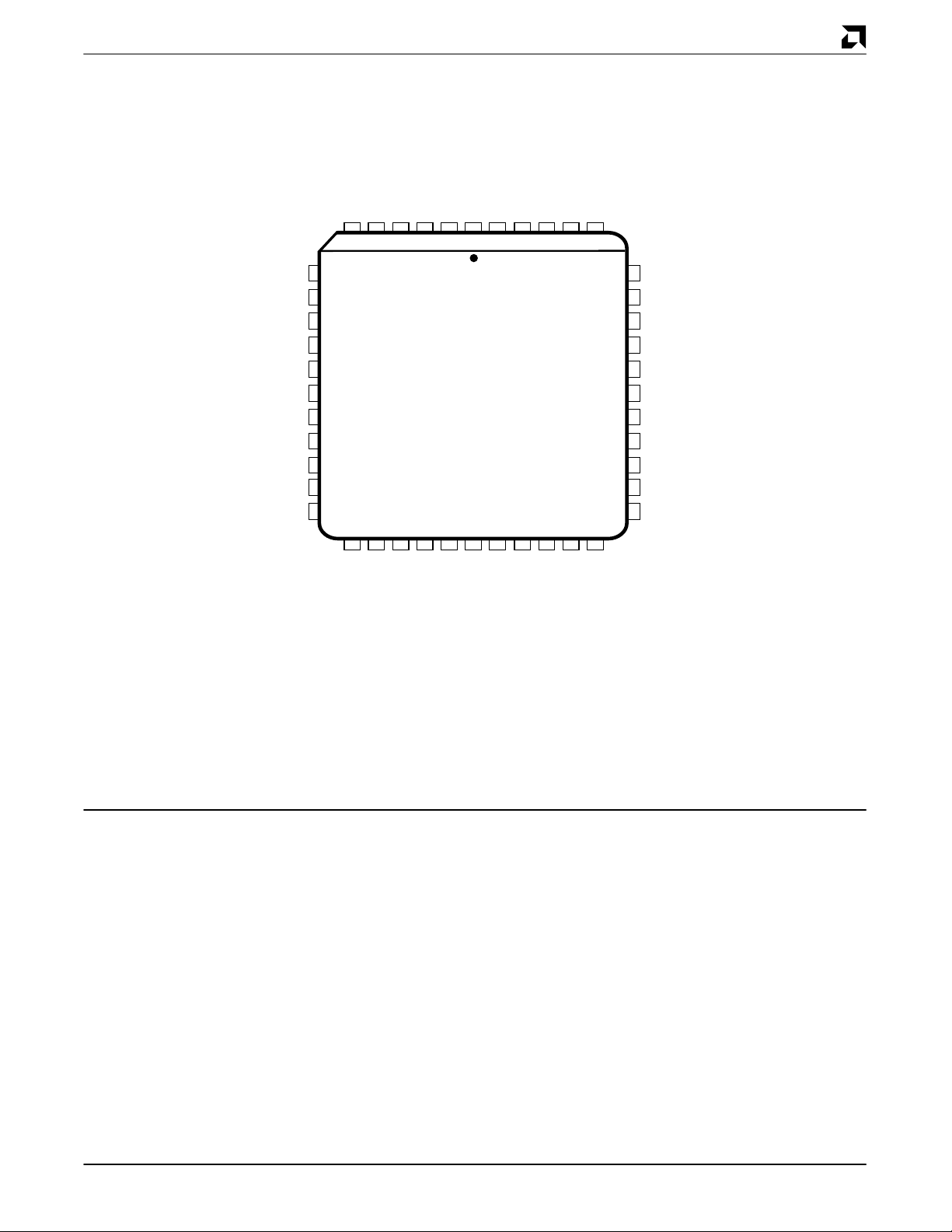
CONNECTION DIAGRAM
Top View
PLCC
14127I-2
I/O
5
I/O
6
I/O
7
I
0
I
1
CLK
0
/I
2
I/O
8
I/O
9
GND
I/O
10
I/O
11
I/O
4
I/O
3
I/O
2
I/O
1
I/O
0
GND
V
CC
I/O
31
I/O
30
I/O
29
I/O
28
I/O
27
I/O
26
I/O
25
I
3
I
4
I/O
24
CLK
1
/I
5
GND
I/O
23
I/O
22
I/O
21
I/O
12
I/O
13
I/O
14
V
CC
GND
I/O
16
I/O
15
I/O
17
I/O
18
I/O
19
I/O
20
7
8
9
10
11
12
13
15
16
14
17
561324 4443424140
29
30
31
32
33
34
35
36
37
38
39
18 282726252423222119 20
PIN DESIGNATIONS
CLK/I = Clock or Input
GND = Ground
I = Input
I/O = Input/Output
V
CC
= Supply Voltage
Note:
Pin-compatible with MACH111, MACH210, MACH211, and MACH215.
AMD
MACH110-12/15/20 (Com’l)4
ORDERING INFORMATION
Commercial Products
Valid Combinations
The Valid Combinations table lists configurations
planned to be supported in volume for this device.
Consult the local AMD sales office to confirm availability
of specific valid combinations and to check on newly
released combinations.
AMD programmable logic products for commercial applications are available with several ordering options. The order number
(Valid Combination) is formed by a combination of:
OPERATING CONDITIONS
C = Commercial (0
°C to +70°C)
FAMILY TYPE
MACH = Macro Array CMOS High-Speed
SPEED
-12 = 12 ns t
PD
-15 = 15 ns t
PD
-20 = 20 ns t
PD
MACH110-12
MACH110-15
MACH110-20
MACH -12 J C
Valid Combinations
OPTIONAL PROCESSING
Blank = Standard Processing
110
DEVICE NUMBER
110 = 32 Macrocells, 44 Pins
PACKAGE TYPE
J = 44-Pin Plastic Leaded
Chip Carrier (PL 044)
JC
AMD
5MACH110-14/18/25 (Ind)
ORDERING INFORMATION
Industrial Products
Valid Combinations
The Valid Combinations table lists configurations
planned to be supported in volume for this device.
Consult the local AMD sales office to confirm availability
of specific valid combinations and to check on newly
released combinations.
AMD programmable logic products for Industrial applications are available with several ordering options. The order number (Valid
Combination) is formed by a combination of:
OPERATING CONDITIONS
I = Industrial (–40°C to +85°C)
FAMILY TYPE
MACH = Macro Array CMOS High-Speed
SPEED
-14 = 14 ns t
PD
-18 = 18 ns t
PD
-24 = 24 ns t
PD
MACH110-14
MACH110-18 JI
MACH110-24
MACH -14 I
Valid Combinations
OPTIONAL PROCESSING
Blank = Standard Processing
110
DEVICE NUMBER
110 = 32 Macrocells, 44 Pins
J
PACKAGE TYPE
J = 44-Pin Plastic Leaded Chip
Carrier (PL 044)
AMD
6 MACH110-12/15/20
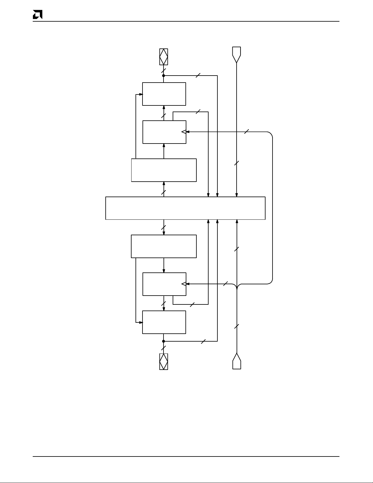
FUNCTIONAL DESCRIPTION
The MACH110 consists of two PAL blocks connected by
a switch matrix. There are 32 I/O pins and 6 dedicated
input pins feeding the switch matrix. These signals are
distributed to the two PAL blocks for efficient design
implementation. There are two clock pins that can also
be used as dedicated inputs.
The PAL Blocks
Each PAL block in the MACH110 (Figure 1) contains a
64-product-term logic array, a logic allocator, 16 macro-
cells and 16 I/O cells. The switch matrix feeds each PAL
block with 22 inputs. This makes the PAL block look
effectively like an independent “PAL22V16”.
There are four additional output enable product terms in
each PAL block. For purposes of output enable, the 16
I/O cells are divided into 2 banks of 8 macrocells. Each
bank is allocated two of the output enable product terms.
An asynchronous reset product term and an asynchro-
nous preset product term are provided for flip-flop
initialization. All flip-flops within the PAL block are
initialized together.
The Switch Matrix
The MACH110 switch matrix is fed by the inputs and
feedback signals from the PAL blocks. Each PAL block
provides 16 internal feedback signals and 16 I/O
feedback signals. The switch matrix distributes these
signals back to the PAL blocks in an efficient manner
that also provides for high performance. The design
software automatically configures the switch matrix
when fitting a design into the device.
The Product-Term Array
The MACH110 product-term array consists of 64
product terms for logic use, and 6 special-purpose
product terms. Four of the special-purpose product
terms provide programmable output enable, one
provides asynchronous reset, and one provides a
synchronous preset. Two of the output enable product
terms are used for the first eight I/O cells; the other two
control the last eight macrocells.
The Logic Allocator
The logic allocator in the MACH110 takes the 64 logic
product terms and allocates them to the 16 macrocells
as needed. Each macrocell can be driven by up to
12 product terms. The design software automatically
configures the logic allocator when fitting the design into
the device.
Table 1 illustrates which product term clusters are
available to each macrocell within a PAL block. Refer to
Figure 1 for cluster and macrocell numbers.
Table 1. Logic Allocation
Available
Output Macrocell Clusters
M
0
C
0
, C
1
M
1
C
0
, C
1
, C
2
M
2
C
1
, C
2
, C
3
M
3
C
2
, C
3
, C
4
M
4
C
3
, C
4
, C
5
M
5
C
4
, C
5
, C
6
M
6
C
5
, C
6
, C
7
M
7
C
6
, C
7
M
8
C
8
, C
9
M
9
C
8
, C
9
, C
10
M
10
C
9
, C
10
, C
11
M
11
C
10
, C
11
, C
12
M
12
C
11
, C
12
, C
13
M
13
C
12
, C
13
, C
14
M
14
C
13
, C
14
, C
15
M
15
C
14
, C
15
The Macrocell
The MACH110 macrocells can be configured as either
registered or combinatorial, with programmable polar-
ity. The macrocell provides internal feedback whether
configured as registered or combinatorial. The flip-flops
can be configured as D-type or T-type, allowing for
product-term optimization.
The flip-flops can individually select one of two clock
pins, which are also available as data inputs. The regis-
ters are clocked on the LOW-to-HIGH transition of the
clock signal. The flip-flops can also be asynchronously
initialized with the common asynchronous reset and
preset product terms.
The I/O Cell
The I/O cell in the MACH110 consists of a three-state
output buffer. The three-state buffer can be configured
in one of three ways: always enabled, always disabled,
or controlled by a product term. If product term control is
chosen, one of two product terms may be used to
provide the control. The two product terms that are
available are common to eight I/O cells. Within each
PAL block, two product terms are available for selection
by the first eight three-state outputs; two other product
terms are available for selection by the last eight
three-state outputs.
These choices make it possible to use the macrocell as
an output, an input, a bidirectional pin, or a three-state
output for use in driving a bus.
AMD
7MACH110-12/15/20
14127I-3
0 4 8 12 16 20 24 28 4032
43
36
0 4 8 12 16 20 24 28 4032
43
36
I/O
Cell
I/O
I/O
I/O
I/O
I/O
I/O
I/O
I/O
I/O
I/O
I/O
I/O
I/O
I/O
I/O
I/O
Switch
Matrix
Output Enable
Output Enable
Asynchronous Reset
Asynchronous Preset
Output Enable
Output Enable
CLK
16
I/O
Cell
I/O
Cell
I/O
Cell
I/O
Cell
I/O
Cell
I/O
Cell
I/O
Cell
I/O
Cell
I/O
Cell
I/O
Cell
I/O
Cell
I/O
Cell
I/O
Cell
I/O
Cell
I/O
Cell
Output
Macro
Cell
Output
Macro
Cell
Output
Macro
Cell
Output
Macro
Cell
Output
Macro
Cell
Output
Macro
Cell
Output
Macro
Cell
Output
Macro
Cell
16
Output
Macro
Cell
Output
Macro
Cell
Output
Macro
Cell
Output
Macro
Cell
Output
Macro
Cell
Output
Macro
Cell
Output
Macro
Cell
Output
Macro
Cell
4
0
Logic Allocator
63
C
0
C
1
C
2
C
3
C
4
C
5
C
6
C
7
C
8
C
9
C
10
C
11
C
12
C
13
C
14
C
15
M
3
M
6
M
5
M
4
M
2
M
1
M
0
M
9
M
8
M
7
M
10
M
11
M
12
M
13
M
14
M
15
Figure 1. MACH110 PAL Block
AMD
MACH110-12/15/20 (Com’l)8
ABSOLUTE MAXIMUM RATINGS
Storage Temperature –65°C to +150°C. . . . . . . . . . .
Ambient Temperature
With Power Applied –55°C to +125°C. . . . . . . . . . . . .
Supply Voltage with
Respect to Ground –0.5 V to +7.0 V. . . . . . . . . . . . .
DC Input Voltage –0.5 V to V
CC
+ 0.5 V. . . . . . . . . . . .
DC Output or I/O
Pin Voltage –0.5 V to V
CC
+ 0.5 V. . . . . . . . . . . . . . . .
Static Discharge Voltage 2001 V. . . . . . . . . . . . . . . .
Latchup Current
(T
A
= 0°C to 70°C) 200 mA. . . . . . . . . . . . . . . . . . . . .
Stresses above those listed under Absolute Maximum Ratings
may cause permanent device failure. Functionality at or above
these limits is not implied. Exposure to Absolute Maximum
Ratings for extended periods may affect device reliability. Pro-
gramming conditions may differ.
OPERATING RANGES
Commercial (C) Devices
Ambient Temperature (T
A
)
Operating in Free Air 0°C to +70°C. . . . . . . . . . . .
Supply Voltage (V
CC
)
with Respect to Ground +4.75 V to +5.25 V. . . . .
Operating ranges define those limits between which the func-
tionality of the device is guaranteed.
DC CHARACTERISTICS over COMMERCIAL operating ranges unless otherwise specified
Parameter
Symbol Parameter Description Test Conditions Min Typ Max Unit
V
OH
Output HIGH Voltage I
OH
= –3.2 mA, V
CC
= Min 2.4 V
V
IN
= V
IH
or V
IL
V
OL
Output LOW Voltage I
OL
= 16 mA, V
CC
= Min 0.5 V
V
IN
= V
IH
or V
IL
V
IH
Input HIGH Voltage Guaranteed Input Logical HIGH 2.0 V
Voltage for all Inputs (Note 1)
V
IL
Input LOW Voltage Guaranteed Input Logical LOW 0.8 V
Voltage for all Inputs (Note 1)
I
IH
Input HIGH Current V
IN
= 5.25 V, V
CC
= Max (Note 2) 10 µA
I
IL
Input LOW Current V
IN
= 0 V, V
CC
= Max (Note 2) –10 µA
I
OZH
Off-State Output Leakage V
OUT
= 5.25 V, V
CC
= Max 10 µA
Current HIGH V
IN
= V
IH
or V
IL
(Note 2)
I
OZL
Off-State Output Leakage V
OUT
= 0 V, V
CC
= Max –10 µA
Current LOW V
IN
= V
IH
or V
IL
(Note 2)
I
SC
Output Short-Circuit Current V
OUT
= 0.5 V, V
CC
= Max (Note 3) –30 –160 mA
I
CC
Supply Current (Typical) V
CC
= 5 V, T
A
=25°C, 95 mA
f = 25 MHz (Note 4)
Notes:
1. These are absolute values with respect to device ground and all overshoots due to system and/or tester noise are included.
2. I/O pin leakage is the worst case of I
IL
and I
OZL
(or I
IH
and I
OZH
).
3. Not more than one output should be shorted at a time. Duration of the short-circuit should not exceed one second.
V
OUT
= 0.5 V has been chosen to avoid test problems caused by tester ground degradation.
4. Measured with a 16-bit up/down counter program. This pattern is programmed in each PAL block and is capable of being
loaded, enabled, and reset.
AMD
9MACH110-12/15/20 (Com’l)
CAPACITANCE (Note 1)
Parameter
Symbol Parameter Description Test Conditions Typ Unit
C
IN
Input Capacitance V
IN
= 2.0 V V
CC
= 5.0 V, T
A
= 25°C6 pF
C
OUT
Output Capacitance V
OUT
= 2.0 V f = 1 MHz 8 pF
SWITCHING CHARACTERISTICS over COMMERCIAL operating ranges (Note 2)
Parameter
Symbol Parameter Description Min Max Min Max Min Max Unit
t
PD
Input, I/O, or Feedback to Combinatorial 12 15 20 ns
Output (Note 3)
71013ns
81114ns
t
H
Hold Time 0 0 0 ns
t
CO
Clock to Output (Note 3) 8 10 12 ns
t
WL
668ns
t
WH
668ns
66.7 50 40 MHz
62.5 47.6 38.5 MHz
f
MAX
76.9 66.6 47.6 MHz
71.4 55.5 43.5 MHz
No Feedback 1/(t
WL
+ t
WH
) 83.3 83.3 62.5 MHz
t
AR
Asynchronous Reset to Registered Output 16 20 25 ns
t
ARW
Asynchronous Reset Width (Note 1) 12 15 20 ns
t
ARR
Asynchronous Reset Recovery Time (Note 1) 8 10 15 ns
t
AP
Asynchronous Preset to Registered Output 16 20 25 ns
t
APW
Asynchronous Preset Width (Note 1) 12 15 20 ns
t
APR
Asynchronous Preset Recovery Time (Note 1) 8 10 15 ns
t
EA
Input, I/O, or Feedback to Output Enable (Note 3) 12 15 20 ns
t
ER
Input, I/O, or Feedback to Output Disable (Note 3) 12 15 20 ns
Notes:
1. These parameters are not 100% tested, but are evaluated at initial characterization and at any time the design is modified
where capacitance may be affected.
2. See Switching Test Circuit, for test conditions.
3. Parameters measured with 16 outputs switching.
Setup Time from Input, I/O, or Feedback
to Clock
-12 -20
Clock Width
D-type
T-type
D-type
T-type
LOW
HIGH
D-type
T-type
Maximum
Frequency
(Note 1)
External Feedback 1/(t
S
+ t
CO
)
Internal Feedback (f
CNT
)
t
S
-15
 Loading...