


 Loading...
AMD M690T/E
Databook
Technical Reference Manual
Rev. 3.10
P/N: 42437_m690t_ds
© 2011 Advanced Micro Devices, Inc
Please note that in this databook, references to "DVI" and "HDMI" refer to the capability of the TMDS interface, multiplexed on the PCI Express® external graphics interface, to enable DVI or HDMI™ through passive enabling circuitries. Any statement in this databook on any DVI or HDMI-related functionality must be understood in that context.
This product incorporates copyright protection technology that is protected by U.S. patents and other intellectual property rights. The use of Rovi Corporation's copy protection technology in the device must be authorized by Rovi Corporation and is intended for home and other limited pay-per-view uses only, unless otherwise authorized in writing by Rovi Corporation. Reverse engineering or disassembly is prohibited.
This device may only be sold or distributed to: (i) a Rovi Authorized Buyer, (ii) a customer (PMA Customer) who has executed a Proprietary Materials Agreement (PMA) with Rovi Corporation that is still in effect, (iii) a contract manufacturer approved by Rovi Coporation to purchase this device on behalf of a Rovi Authorized Buyer or a PMA Customer, or (iv) a distributor who has executed a Rovi-specified distribution agreement with AMD.
Trademarks
AMD, the AMD Arrow logo, AMD Athlon, AMD Sempron, AMD Turion, Cool'n'Quiet, AMD PowerNow!, AMD Radeon, AMD Avivo, AMD HyperMemory, PowerPlay, PowerShift, AMD PowerXpress, and combinations thereof, are trademarks of Advanced Micro Devices, Inc.
HDMI is a trademark of HDMI Licensing, LLC.
HyperTransport is a licensed trademark of the HyperTransport Technology Consortium.
Microsoft, Windows, Windows Vista, and DirectX are registered trademarks of Microsoft Corporation.
PCI Express and PCIe are registered trademarks of PCI-SIG.
WinBench is a registered trademark of Ziff Davis, Inc.
Other product names used in this publication are for identification purposes only and may be trademarks of their respective companies.
Disclaimer
The contents of this document are provided in connection with Advanced Micro Devices, Inc. ("AMD") products. AMD makes no representations or warranties with respect to the accuracy or completeness of the contents of this publication and reserves the right to make changes to specifications and product descriptions at any time without notice. AMD assumes no liability whatsoever, and disclaims any express or implied warranty, relating to this document including, but not limited to, the implied warranty of merchantability, fitness for a particular purpose, or infringement of any intellectual property right. AMD shall not be liable for any damage, loss, expense, or claim of loss of any kind or character (including without limitation direct, indirect, consequential, exemplary, punitive, special, incidental or reliance damages) arising from use of or reliance on this document. No license, whether express, implied, arising by estoppel, or otherwise, to any intellectual property rights are granted by this publication. Except for AMD product purchased pursuant to AMD's Standard Terms and Conditions of Sale, and then only as expressly set forth therein, AMD's products are not designed, intended, authorized or warranted for use as components in systems intended for surgical implant into the body, or in other applications intended to support or sustain life, or in any other application in which the failure of AMD's product could create a situation where personal injury, death, or severe property or environmental damage may occur. AMD reserves the right to discontinue or make changes to its products at any time without notice.
© 2011 Advanced Micro Devices, Inc. All rights reserved.

Table of Contents
Chapter 1: Overview
1.1 |
Introducing the M690T ....................................................................................................................................................... |
1-1 |
|
1.2 |
M690E |
................................................................................................................................................................................. |
1-2 |
1.3 |
M690T ..................................................................................................................................................................Features |
1-2 |
|
|
1.3.1 ......................................................................................................................... |
CPU HyperTransport™ Interface |
1-2 |
|
1.3.2 ................................................................................................................................................. |
Memory Interface |
1-2 |
|
1.3.3 .................................................................................................................... |
AMD HyperMemory™ Technology |
1-2 |
|
1.3.4 ....................................................................................................................................... |
PCI Express® Interface |
1-2 |
|
1.3.5 .................................................................................................................................. |
A - Link Express II Interface |
1-3 |
|
1.3.6 ..................................................................................................................................... |
2D Acceleration Features |
1-3 |
|
1.3.7 ..................................................................................................................................... |
3D Acceleration Features |
1-3 |
|
1.3.8 .................................................................................................................... |
Motion Video Acceleration Features |
1-4 |
|
1.3.9 .................................................................................................................................... |
Multiple Display Features |
1-4 |
|
1.3.10 .................................................................................................................................................. |
Integrated LVDS |
1-5 |
|
1.3.11 ....................................................................................................................................................... |
DVI/HDMI™ |
1-6 |
|
1.3.12 ...................................................................................................................... |
External Display Support via DVO |
1-6 |
|
1.3.13 ............................................................................................................................... |
Power Management Features |
1-6 |
|
1.3.14 .............................................................................................................................. |
PC Design Guide Compliance |
1-6 |
|
1.3.15 ....................................................................................................................................... |
Test Capability Features |
1-7 |
|
1.3.16 .............................................................................................................................................. |
Additional Features |
1-7 |
|
1.3.17 ............................................................................................................................................................. |
Packaging |
1-7 |
1.4 |
Software ................................................................................................................................................................Features |
1-7 |
|
1.5 |
Device ...........................................................................................................................................................................IDs |
1-8 |
|
1.6 |
Branding .............................................................................................................................................................Diagrams |
1-8 |
|
|
1.6.1 ......................................................................................................... |
Branding Diagram for ASIC Revision A11 |
1-8 |
|
1.6.2 ......................................................................................... |
Branding Diagram for ASIC Revision A12 and After |
1-8 |
1.7 |
Part Number .........................................................................................................................................................Legend |
1-10 |
|
1.8 |
Production .................................................................................................................Schedule, OPN, and Part Marking |
1-10 |
|
1.9 |
Conventions ...............................................................................................................................................and Notations |
1-10 |
|
|
1.9.1 ........................................................................................................................................................... |
Pin Names |
1-10 |
|
1.9.2 ............................................................................................................................................................ |
Pin Types |
1-10 |
|
1.9.3 ..................................................................................................................................... |
Numeric Representation |
1-11 |
|
1.9.4 ...................................................................................................................................................... |
Register Field |
1-11 |
|
1.9.5 .......................................................................................................................................................... |
Hyperlinks |
1-11 |
|
1.9.6 ............................................................................................................................. |
Acronyms and Abbreviations |
1-11 |
Chapter 2: Functional Descriptions
2.1 |
Host Interface...................................................................................................................................................................... |
2-2 |
|
2.2 |
Side-port Memory Interface................................................................................................................................................ |
2-3 |
|
|
2.2.1 |
DDR2 Memory Interface...................................................................................................................................... |
2-3 |
2.3 |
LVDS Interface ................................................................................................................................................................... |
2-6 |
|
|
2.3.1 |
LVDS Data Mapping............................................................................................................................................ |
2-6 |
© 2011 Advanced Micro Devices, Inc. |
42437 AMD M690T/E Databook 3.10 |
Proprietary |
Table of Contents-1 |

|
2.3.2 LVDS Spread Spectrum ...................................................................................................................................... |
2-8 |
2.4 |
DVI/HDMI™ ..................................................................................................................................................................... |
2-9 |
|
2.4.1 DVI/HDMI™ Data Transmission Order and Signal Mapping............................................................................ |
2-9 |
|
2.4.2 Support for HDMI™ Packet Types................................................................................................................... |
2-12 |
2.5 |
VGA DAC Characteristics ............................................................................................................................................... |
2-13 |
2.6 |
External Clock Chip ......................................................................................................................................................... |
2-13 |
Chapter 3: Pin Descriptions and Strap Options
3.1 |
Pin Assignment .................................................................................................................................................................. |
3-2 |
|
|
3.1.1 |
M690T Pin Assignment....................................................................................................................................... |
3-2 |
3.2 |
Interface Block Diagram .................................................................................................................................................... |
3-4 |
|
3.3 |
CPU HyperTransport™ Interface .................................................................................................................................... |
3-5 |
|
3.4 |
DDR2 Side-port Memory Interface.................................................................................................................................... |
3-5 |
|
3.5 |
PCI Express® Interfaces .................................................................................................................................................... |
3-6 |
|
|
3.5.1 |
1 x 8 Lane Interface for External Graphics ......................................................................................................... |
3-6 |
|
3.5.2 |
A-Link Express II to Southbridge........................................................................................................................ |
3-6 |
|
3.5.3 |
4 x 1 Lane Interface for General Purpose External Devices .............................................................................. |
3-6 |
|
3.5.4 |
Miscellaneous PCI Express® Signals ................................................................................................................. |
3-7 |
3.6 |
Clock Interface ................................................................................................................................................................... |
3-7 |
|
3.7 |
CRT and TV Interface........................................................................................................................................................ |
3-7 |
|
3.8 |
LVDS Interface (24 Bits) ................................................................................................................................................... |
3-8 |
|
3.9 |
DVO Interface for External Display .................................................................................................................................. |
3-9 |
|
3.10 TMDS Interface Multiplexed on the PCI Express® Graphics Lanes ............................................................................ |
3-10 |
||
3.11 |
Power Management Pins................................................................................................................................................ |
3-11 |
|
3.12 |
Miscellaneous Pins.......................................................................................................................................................... |
3-11 |
|
3.13 Power Pins...................................................................................................................................................................... |
3-12 |
||
3.14 Ground Pins.................................................................................................................................................................... |
3-13 |
||
3.15 |
Debug Port Signals......................................................................................................................................................... |
3-13 |
|
3.16 |
Strapping Options........................................................................................................................................................... |
3-14 |
|
Chapter 4: Timing Specifications
4.1 |
CPU HyperTransport™ Bus Timing.................................................................................................................................. |
4-1 |
4.2 |
HyperTransport™ Reference Clock Timing Parameters ................................................................................................... |
4-1 |
4.3 |
PCI Express® Differential Clock AC Specifications......................................................................................................... |
4-1 |
4.4 |
Side-port Memory Timing ................................................................................................................................................. |
4-1 |
|
4.4.1 Read Cycle DQ/DQS Delay ................................................................................................................................ |
4-1 |
|
4.4.2 Write Cycle DQ/DQS Delay ............................................................................................................................... |
4-2 |
4.5 |
LVDS Timing..................................................................................................................................................................... |
4-2 |
4.6 |
OSCIN Timing ................................................................................................................................................................... |
4-2 |
4.7 |
Power Rail Power Up Sequence......................................................................................................................................... |
4-4 |
4.8 |
LCD Panel Power Up/Down Timing ................................................................................................................................. |
4-5 |
42437 AMD M690T/E Databook 3.10 |
© 2011 Advanced Micro Devices, Inc. |
Table of Contents-2 |
Proprietary |

Chapter 5: Electrical Characteristics and Physical Data
5.1 |
Electrical Characteristics..................................................................................................................................................... |
5-1 |
|
|
5.1.1 |
Maximum and Minimum Ratings ........................................................................................................................ |
5-1 |
|
5.1.2 |
DC Characteristics................................................................................................................................................ |
5-2 |
5.2 |
M690T Thermal Characteristics ......................................................................................................................................... |
5-5 |
|
|
5.2.1 |
M690T Thermal Limits ........................................................................................................................................ |
5-5 |
|
5.2.2 |
Thermal Diode Characteristics............................................................................................................................. |
5-6 |
5.3 |
Package Information ........................................................................................................................................................... |
5-7 |
|
|
5.3.1 |
Physical Dimensions ............................................................................................................................................ |
5-7 |
|
5.3.2 |
Pressure Specification .......................................................................................................................................... |
5-9 |
|
5.3.3 |
Board Solder Reflow Process Recommendations ................................................................................................ |
5-9 |
Chapter 6: Power Management and ACPI
6.1 |
ACPI Power Management Implementation ........................................................................................................................ |
6-1 |
|
6.2 |
Power Management for the Graphics Controller ................................................................................................................ |
6-2 |
|
|
6.2.1 |
PCI Function Power States................................................................................................................................... |
6-2 |
|
6.2.2 |
PCI Power Management Interface........................................................................................................................ |
6-2 |
|
6.2.3 |
Capabilities List Data Structure in PCI Configuration Space .............................................................................. |
6-2 |
|
6.2.4 |
Register Block Definition..................................................................................................................................... |
6-3 |
|
6.2.5 |
Capability Identifier: Cap_ID (Offset = 0)........................................................................................................... |
6-4 |
|
6.2.6 |
Next Item Pointer ................................................................................................................................................. |
6-5 |
|
6.2.7 |
PMC - Power Management Capabilities (Offset = 2) .......................................................................................... |
6-5 |
Chapter 7: Testability
7.1 |
Test Capability Features...................................................................................................................................................... |
7-1 |
|
7.2 |
Test Interface....................................................................................................................................................................... |
7-1 |
|
7.3 |
XOR Tree............................................................................................................................................................................ |
7-1 |
|
|
7.3.1 Brief Description of an XOR Tree ....................................................................................................................... |
7-1 |
|
|
7.3.2 Description of the XOR Tree for the M690T....................................................................................................... |
7-2 |
|
|
7.3.3 |
XOR Tree Activation ........................................................................................................................................... |
7-2 |
|
7.3.4 XOR Chain for the M690T................................................................................................................................... |
7-2 |
|
7.4 |
VOH/VOL Test................................................................................................................................................................... |
7-4 |
|
|
7.4.1 Brief Description of a VOH/VOL Tree................................................................................................................ |
7-4 |
|
|
7.4.2 |
VOH/VOL Tree Activation.................................................................................................................................. |
7-4 |
|
7.4.3 |
VOH/VOL Pin List............................................................................................................................................... |
7-5 |
Appendix A: Pin Listings
A.1 |
M690T |
Pin List Sorted by Ball Reference........................................................................................................................ |
1-2 |
A.2 |
M690T |
Pin List Sorted by Pin Name................................................................................................................................ |
1-6 |
Appendix B: AMD M690E
B.1 |
Introduction ....................................................................................................................................................................... |
2-1 |
B.2 |
Feature Differences between the M690T and M690E ...................................................................................................... |
2-1 |
B.3 |
DVI-I Support.................................................................................................................................................................... |
2-3 |
B.4 |
HDMI™ ............................................................................................................................................................................ |
2-3 |
© 2011 Advanced Micro Devices, Inc. |
42437 AMD M690T/E Databook 3.10 |
Proprietary |
Table of Contents-3 |

B.5 |
HDCP................................................................................................................................................................................. |
2-4 |
B.6 |
M690E Display Options .................................................................................................................................................... |
2-4 |
B.7 |
The LVTM Interface in TMDS Mode............................................................................................................................... |
2-5 |
Appendix C: Revision History
42437 AMD M690T/E Databook 3.10 |
© 2011 Advanced Micro Devices, Inc. |
Table of Contents-4 |
Proprietary |

List of Figures
Figure 1-1: M690T Branding Diagram for ASIC Revision A11 ..................................................................................................... |
1-8 |
Figure 1-2: M690T Branding Diagram for ASIC Revision A12 ..................................................................................................... |
1-9 |
Figure 1-3: M690T ASIC Part Number Legend ............................................................................................................................ |
1-10 |
Figure 2-1: M690T Internal Block Diagram .................................................................................................................................... |
2-1 |
Figure 2-2: Host Interface Block Diagram ...................................................................................................................................... |
2-2 |
Figure 2-3: M690T Host Bus Interface Signals .............................................................................................................................. |
2-3 |
Figure 2-4: M690T Side-port Memory Interface ............................................................................................................................. |
2-4 |
Figure 2-5: Single/Dual Channel 24-bit LVDS Data Transmission Ordering ................................................................................. |
2-6 |
Figure 2-6: Data Transmission Ordering for the TMDS Interface .................................................................................................. |
2-9 |
Figure 3-1: M690T Pin Assignment (Left) ...................................................................................................................................... |
3-2 |
Figure 3-2: M690T Pin Assignment (Right) .................................................................................................................................... |
3-3 |
Figure 3-3: M690T Interface Block Diagram .................................................................................................................................. |
3-4 |
Figure 4-1: Power Rail Power Up Sequence for the M690T ........................................................................................................... |
4-4 |
Figure 4-2.: LCD Panel Power Up/Down Timing ........................................................................................................................... |
4-5 |
Figure 5-1: DC Characteristics of the TMDS Interface ................................................................................................................... |
5-4 |
Figure 5-2: DC Characteristics of the LVDS Interface ................................................................................................................... |
5-5 |
Figure 5-3: M690T Package Outline ............................................................................................................................................... |
5-7 |
Figure 5-4: M690T Ball Arrangement ............................................................................................................................................. |
5-8 |
Figure 5-5: Stencil Opening Recommendations .............................................................................................................................. |
5-9 |
Figure 5-6: RoHS/Lead-Free Solder (SAC305/405 Tin-Silver-Copper) Reflow Profile .............................................................. |
5-10 |
Figure 6-1: Linked List for Capabilities .......................................................................................................................................... |
6-5 |
Figure 7-1: An Example of a Generic XOR Tree ............................................................................................................................ |
7-1 |
Figure 7-2: Sample of a Generic VOH/VOL Tree ........................................................................................................................... |
7-4 |
Figure B-1: M690E Branding Diagram for ASIC Revision A12 .................................................................................................... |
2-1 |
Figure B-2: M690T and M690E Analog Display Output Signals ................................................................................................... |
2-2 |
Figure B-3: M690E LVTM Interface .............................................................................................................................................. |
2-3 |
Figure B-4: Pins for Analog Output on the DVI-I Connector ......................................................................................................... |
2-3 |
Figure B-5: M690E Display Options ............................................................................................................................................... |
2-4 |
Figure B-6: DC Characteristics of the LVTM Interface in TMDS Mode ....................................................................................... |
2-7 |
42437 AMD M690T/E Databook 3.10 |
© 2011 Advanced Micro Devices, Inc. |
List of Figures-1 |
Proprietary |

This page is left blank intentionally.
42437 AMD M690T/E Databook 3.10 |
© 2011 Advanced Micro Devices, Inc. |
List of Figures-2 |
Proprietary |

List of Tables
Table 1-1: M690T Device IDs ........................................................................................................................................................ |
1-8 |
Table 1-2: M690T Planned production Schedule, OPN, and Part Marking ................................................................................. |
1-10 |
Table 1-3: Pin Type Codes ........................................................................................................................................................... |
1-11 |
Table 1-4: Acronyms and Abbreviations ...................................................................................................................................... |
1-11 |
Table 2-1: Supported DDR2 Components ...................................................................................................................................... |
2-4 |
Table 2-2: DDR2 Memory Row and Column Addressing ............................................................................................................. |
2-4 |
Table 2-3: LVDS 24-bit TFT Single Pixel per Clock (Single Channel) Signal Mapping .............................................................. |
2-7 |
Table 2-4: LVDS 24-bit TFT Dual Pixel per Clock (Dual Channel) Signal Mapping ................................................................... |
2-8 |
Table 2-5: Single-Link Signal Mapping for DVI/HDMI™ ......................................................................................................... |
2-10 |
Table 2-6: Dual-Link Signal Mapping for DVI ............................................................................................................................ |
2-11 |
Table 2-7: Support for HDMI™ Packet Type .............................................................................................................................. |
2-12 |
Table 2-8: VGA DAC Characteristics .......................................................................................................................................... |
2-13 |
Table 3-1: CPU HyperTransport™ Interface .................................................................................................................................. |
3-5 |
Table 3-2: DDR2 Side-port Memory Interface ............................................................................................................................... |
3-5 |
Table 3-3: 1 x 8 Lane PCI Express® Interface for External Graphics ........................................................................................... |
3-6 |
Table 3-4: 1 x 4 Lane A-Link Express II Interface for Southbridge .............................................................................................. |
3-6 |
Table 3-5: 4 x 1 Lane PCI Express® Interface for General Purpose External Devices ................................................................. |
3-6 |
Table 3-6: PCI Express® Interface for Miscellaneous PCI Express® Signals .............................................................................. |
3-7 |
Table 3-7: Clock Interface .............................................................................................................................................................. |
3-7 |
Table 3-8: CRT and TV Interface ................................................................................................................................................... |
3-7 |
Table 3-9: LVDS Interface ............................................................................................................................................................. |
3-8 |
Table 3-10: DVO Interface ............................................................................................................................................................. |
3-9 |
Table 3-11: TMDS Interface Multiplexed on the PCI Express® Graphics Interface ................................................................... |
3-10 |
Table 3-12: Power Management Pins ........................................................................................................................................... |
3-11 |
Table 3-13: Miscellaneous Pins .................................................................................................................................................... |
3-11 |
Table 3-14: Power Pins ................................................................................................................................................................. |
3-12 |
Table 3-15: Ground Pins ............................................................................................................................................................... |
3-13 |
Table 3-16: M690T Debug Port Signals ....................................................................................................................................... |
3-13 |
Table 3-17: Strap Definitions for the M690T ............................................................................................................................... |
3-14 |
Table 3-18: Strap Definition for GPPSB_LINK_CONFIG .......................................................................................................... |
3-15 |
Table 4-1: HTREFCLK Pad (66.66MHz) Timing Parameters ....................................................................................................... |
4-1 |
Table 4-2: PCI Express® Differential Clock (GFX_CLK, SB_CLK) AC Characteristics ............................................................ |
4-1 |
Table 4-3: Timing Requirements for the LVDS Interface .............................................................................................................. |
4-2 |
Table 4-4: Timing Requirements for the OSCIN Pad .................................................................................................................... |
4-2 |
Table 4-5: M690T Power Rail Power Up Sequence Requirements ............................................................................................... |
4-4 |
Table 4-6: LCD Power Up/Down Timing ...................................................................................................................................... |
4-5 |
Table 5-1: Maximum and Minimum Ratings ................................................................................................................................. |
5-1 |
Table 5-2: DC Characteristics for 3.3V TTL Signals ..................................................................................................................... |
5-2 |
Table 5-3: DC Characteristics for 1.8V TTL Signals ..................................................................................................................... |
5-2 |
Table 5-4: DC Characteristics for the HTREFCLK Pad (66.66MHz) ............................................................................................ |
5-2 |
Table 5-5: DC Characteristics for the OSCIN Pad (14.3181818MHz) .......................................................................................... |
5-2 |
Table 5-6: DC Characteristics for the DDR2 Interface .................................................................................................................. |
5-3 |
Table 5-7: DC Characteristics for the TMDS Interface Multiplexed on the PCI Express® Gfx Lanes ......................................... |
5-3 |
Table 5-8: Electrical Requirements for the LVDS Interface .......................................................................................................... |
5-4 |
Table 5-9: M690T Thermal Limits ................................................................................................................................................. |
5-5 |
Table 5-10: M690T 465-Pin FCBGA Package Physical Dimensions ............................................................................................ |
5-7 |
Table 5-11: Recommended Board Solder Reflow Profile - RoHS/Lead-Free Solder .................................................................. |
5-10 |
Table 6-1: ACPI States Supported by the M690T .......................................................................................................................... |
6-1 |
Table 6-2: ACPI Signal Definitions ................................................................................................................................................ |
6-1 |
42437 AMD M690T/E Databook 3.10 |
© 2011 Advanced Micro Devices, Inc. |
List of Tables-1 |
Proprietary |

Table 6-3: Standard PCI Configuration Space Header Type 0 ...................................................................................................... |
6-2 |
Table 6-4: PCI Status Register ....................................................................................................................................................... |
6-3 |
Table 6-5: Capabilities Pointer (CAP_PTR) .................................................................................................................................. |
6-3 |
Table 6-6: Power Management Register Block .............................................................................................................................. |
6-3 |
Table 6-7: Power Management Control/Status Register (PMCSR) ............................................................................................... |
6-4 |
Table 6-8: Capability Identifier (Cap_ID) ...................................................................................................................................... |
6-4 |
Table 6-9: Next Item Pointer (NEXT_ITEM_PTR) ....................................................................................................................... |
6-5 |
Table 6-10: Power Management Capabilities – PMC .................................................................................................................... |
6-5 |
Table 7-1: Pins on the Test Interface .............................................................................................................................................. |
7-1 |
Table 7-2: Example of an XOR Tree .............................................................................................................................................. |
7-2 |
Table 7-3: M690T XOR Tree ......................................................................................................................................................... |
7-2 |
Table 7-4: Truth Table for the VOH/VOL Tree Outputs ............................................................................................................... |
7-4 |
Table 7-5: M690T VOH/VOL Tree ............................................................................................................................................... |
7-5 |
42437 AMD M690T/E Databook 3.10 |
© 2011 Advanced Micro Devices, Inc. |
List of Tables-2 |
Proprietary |
Chapter 1
Overview
1.1Introducing the M690T
The M690T is a seventh generation Integrated Graphics Processor (IGP) that integrates a DirectX® 9.0 compliant 2D/3D graphics core and a system controller in a single chip. It is designed to support the AMD Athlon™ 64, AMD Athlon 64 FX, AMD Athlon 64 X2, AMD Sempron™, and AMD Turion™ 64 processors, including both AM2 and S1 socket CPUs. The CPUs are supported on both high performance and value platforms.
The M690T integrates an AMD Radeon™ X1270 graphics engine, dual display, a TV encoder, an LVDS interface, an integrated TMDS controller, and Northbridge functionality in a single BGA package. This high level of integration and scalability is designed to enable manufacturers to offer enthusiast level capabilities and performance while minimizing board space and system cost.
Robust and Flexible Core Logic Features
The M690T combines graphics and system logic functions in a single chip using a 21mm-body FCBGA package, minimizing overall solution area. For optimal system and graphics performance, the M690T supports a high speed HyperTransport™ interface to the AMD processor, running at a data rate of up to 2GT/s and supporting the new generation of AM2 and S1 socket processors. The M690T is ideally suited to 64-bit operating systems, and supports
platform configurations with greater than 4GB of system memory. The rich PCI Express® expansion capabilities of M690T, including support for PCI Express external graphics and up to four other PCI Express peripherals, are complemented by the advanced I/O features of AMD's SB600 Southbridge.
Support for Windows Vista®
The M690T delivers an excellent Windows Vista® experience of any integrated graphics and core logic product for the AMD platform. It incorporates an AMD Radeon™ X700-based graphics core, which provides 3D rendering power to generate the Windows Vista desktop even under demanding circumstances. In addition, dedicated hardware acceleration is provided for key new Windows Vista features such as ClearType. This AMD Radeon X700-based graphics technology also enables great 3D application performance through SmartShader HD, SmoothVision HD, and 3Dc technologies.
Multimedia Capabilities
The M690T incorporates the innovative AMD Avivo™* display architecture, providing users with excellent visual quality. Advanced scaling and color correction capabilities, along with precision through the entire display pipeline, ensure an optimal image on CRT monitors, LCD panels, and any other display devices. A TV encoder provides superior quality, and a TMDS interface, configurable to support DVI/HDMI™ and HDCP, allows compatibility with modern high definition televisions.
*Note: AMD Avivo™ is a technology platform that includes a broad set of capabilities offered by certain AMD Radeon products. Full enablement of some AMD Avivo capabilities may require complementary products.
Low Power Consumption and Industry Leading Power Management
The M690T is manufactured using a power efficient 80nm technology, and it supports a wide range of industry standards and proprietary power management features. In addition to comprehensive support for the ACPI specification and AMD features such as AMD PowerNow!™, the PowerPlay™ technology (enhanced with new adaptive frame buffer compression and PowerShift™ features) minimizes the M690T's power consumption by adjusting graphics core performance and core voltage to the task and usage environment.
Software Compatibility
The graphics driver for the M690T is compatible with AMD Radeon class graphics controllers from AMD. A single driver can support multiple graphics configurations across AMD's product lines, including the AMD Radeon family and the AMD chipset family. In addition, this driver compatibility allows the M690T to benefit immediately from AMD's
© 2011 Advanced Micro Devices, Inc. |
42437 AMD M690T/E Databook 3.10 |
Proprietary |
1-1 |

M690E
software optimization and from the advanced Windows® XP and Windows Vista support available in the AMD Radeon family drivers.
Note: In some reference documents, the M690T is referred to by its code name "RS690T," which signifies the same device.
1.2M690E
The M690T and M690E are the same device with respect to their form, fit, and functionally, except for the differences described in Appendix B, “AMD M690E.” All information in this databook, unless superseded by the information given in Appendix B, is applicable to the M690E.
1.3M690T Features
1.3.1CPU HyperTransport™ Interface
•Supports the mobile and desktop AMD Athlon 64/AMD Athlon 64 FX/AMD Athlon X2/AMD Sempron/AMD Turion 64 processors, including both AM2 and S1 socket CPUs.
•Supports 200, 400, 600, 800, and 1000MHz HyperTransport (HT) interface speeds.
•Supports LDTSTP interface, CPU throttling, and stutter mode.
1.3.2Memory Interface
•Supports an optional dedicated local frame buffer (side-port) of up to 128MB through a 16-bit interface.
•Highly flexible memory architecture allows asymmetric side-port and shared system memory frame buffer sizes.
•Dynamic memory allocation scheme improves performance and reduces power.
•Support for DDR2 system memories up to DDR2-800, with a maximum memory clock speed of 400MHz. Memory clock is independent of any other clock source and can therefore be set to any frequency equal to or less than 400MHz (DDR2-800), allowing the use of lower speed side-port memories.
•Support for 16Mx16, 32Mx8, 32Mx16, 64Mx8, and 64Mx16 memory devices.
•Asynchronous HyperTransport and memory controller interface speeds.
•Supports DDR SDRAM self refresh mechanism.
•Supports dynamic CKE and ODT for power conservation.
1.3.3AMD HyperMemory™ Technology
•Supports AMD HyperMemory™* technology.
* Note: The amount of HyperMemory available includes both dedicated and shared memory and is determined by various factors. For details, please refer to the product advisory numbered PA_IGPGenC5, available on AMD’s OEM Resource Center or from your AMD CSS representative.
1.3.4PCI Express® Interface
•Compliant with the PCI Express (PCIe®) 1.1a Specification.
•Highly flexible PCIe implementation to suit a variety of platform needs.
•A x8 graphics interface, configurable to any of the following modes of support:
•An external graphics device utilizing all 8 lanes (see section 1.3.11“DVI/HDMI™” on page 1-6 for details).
•A TMDS interface, enabling DVI/HDMI.
•A single x1, x2, x4, or x8 general purpose PCIe link.
•Supports programmable lane reversal for the graphics link to ease motherboard layout when the end device does not support lane reversal.
•A four-port, x4 PCI Express general purpose interface, configurable to one of the following modes of support:
42437 AMD M690T/E Databook 3.10 |
© 2011 Advanced Micro Devices, Inc. |
1-2 |
Proprietary |

M690T Features
•Four x1 links.
•Two x2 links.
•One x2 and two x1 links.
•One x4 link.
1.3.5A-Link Express II Interface
•One x4 A-Link Express II interface (PCI Express 1.1 compliant) for connection to an AMD Southbridge, providing more bandwidth than the older A-Link Express interface.
1.3.62D Acceleration Features
•Highly-optimized 128-bit engine, capable of processing multiple pixels per clock.
•Hardware acceleration of Bitblt, Line Draw, Polygon / Rectangle Fill, Bit Masking, Monochrome Expansion, Panning/Scrolling, Scissoring, and full ROP support (including ROP3).
•Optimized handling of fonts and text using AMD proprietary techniques.
•Hardware acceleration for ClearType font rendering.
•Game acceleration including support for Microsoft's DirectDraw: Double Buffering, Virtual Sprites, Transparent Blit, and Masked Blit.
•Acceleration in 1/8/15/16/32 bpp modes:
•ClearType mode for 1bpp
•Pseudocolor mode for 8bpp
•ARGB1555 and RGB565 modes for 16bpp
•ARGB8888 mode for 32bpp
•Significant increase in the High-End Graphics WinBench® score due to capability for C18 color expansion.
•Setup of 2D polygons and lines.
•Support for GDI extensions in Windows XP and Windows Vista: Alpha BLT, Transparent BLT, Gradient Fill.
•Hardware cursor (up to 64x64x32bpp), with alpha channel for direct support of Windows XP and Windows Vista alpha cursor.
1.3.73D Acceleration Features
•Multi-texturing via one texture blending unit per pixel pipes, allowing up to 512 texel reads per pixel in a single pass.
•3D texture support, including projective 3D textures.
•Comprehensive support for bump mapping: emboss, dot-product, and environment bump maps.
•Precision in anisotropic filtering and bilinear filtering.
•3D primitive support: points, lines, triangles, lists, strips and quadrilaterals and BLTs with Z compare.
•Texture compositing.
•Hidden surface removal using 16, 24, or 32-bit Z-buffering (maximum Z-buffer depth is 24 bits when stencil buffer enabled) and Early Z hardware.
•8-bit stencil buffer.
•Bilinear and trilinear texture filtering.
•Support of Direct3D texture lighting.
•Dithering support in 16bpp for near 24bpp quality in less memory.
•Extensive 3D mode support.
•Anti-aliasing using multi-sampling algorithm with support for 2, 4, and 6 samples.
•Optimized for performance in true color triple buffered 32bpp acceleration modes.
© 2011 Advanced Micro Devices, Inc. |
42437 AMD M690T/E Databook 3.10 |
Proprietary |
1-3 |

M690T Features
•New generation rendering engine provides top 3D performance.
•Support for OpenGL format for Indirect Vertices in Vertex Walker.
•DirectX 9.0 support (Vertex Shader version 2.0 and Pixel Shader version 2.0):
•Full precision floating point pixel pipeline.
•Support for up to 4 MRTs (Multiple-Render-Targets).
•Support for writing all texture formats from render pipe in floating points (including cube mapes and 3D textures).
•Support for up to 512bpp formats (4 color case).
•Advanced setup engine, capable of processing 1 polygon (lit and textured) per cycle.
1.3.8Motion Video Acceleration Features
•Enhanced MPEG-2 hardware decode acceleration (SD contents only), including support for:
•Integrated general purpose iDCT engine for MPEG2 and DV decode acceleration.
•Integrated MPEG motion compensation engine for decode acceleration.
•Parallel operation of the iDCT and MC and high processing rates with minimal software overhead.
•Supports Microsoft® DirectX Video Acceleration (DirectX VA) 2.0 (for SD contents only).
•Provides reduced CPU utilization without incurring the cost of a full MPEG-2 decoder.
•MPEG-4 simple profile support.
•Supports top quality DVD with low CPU usage.
•Hardware-based adaptive de-interlacing filter and scaler provide high quality full-screen and full-speed video playback. Minimizes the aliasing artifacts along edges usually caused by a conventional deinterlacer/scaler.
1.3.9Multiple Display Features
General
•Dual independent displays. Possible configurations include:
•CRT and LVDS
•CRT and DVI/HDMI*
•LVDS and DVI/HDMI*
•LVDS and TV (component, composite, or S-Video)
•DVI/HDMI and TV (component, composite, or S-Video)*
•Dual CRT**
•Dual TV**
•CRT and TV**
Notes: * The options require implementation of the TMDS interface that is multiplexed on the PCIe external graphics interface; see section 1.3.11, “DVI/HDMI™,” on page 1-6.
** The options require implementation of the DVO interface for an external display; see section 1.3.12, “External Display Support via DVO,” on page 1-6.
•Resolution, refresh rates, and display data can be completely independent for the two display paths.
•Each display controller supports true 30bpp throughout the display pipeline.
•Each display path supports VGA and accelerated modes, video overlay, hardware cursor, hardware icon, and palette gamma correction.
•Supports both interlaced and non-interlaced displays.
42437 AMD M690T/E Databook 3.10 |
© 2011 Advanced Micro Devices, Inc. |
1-4 |
Proprietary |

M690T Features
•Full ratiometric expansion ability is supported for source desktop modes up to 1920 pixels/line.
•Maximum DAC frequency of 400MHz.
•Supports 8, 16, 32 & 64-bpp depths for the main graphics layer:
•For 32-bpp depth, supports xRGB 8:8:8:8, xRGB 2:10:10:10, sCrYCb 8:8:8:8, and xCrYCb 2:10:10:10 data formats.
•For 64-bpp depth, supports xRGB 16:16:16:16 data format.
•Independent gamma, color conversion and correction controls for main graphics layer.
•Support for DDC1 and DDC2B+ for plug and play monitors.
•8-bit alpha blending of graphics and video overlay.
•Hardware cursor up to 64x64 pixels in 2bpp, full color AND/XOR mix, and full color 8-bit alpha blend.
•Hardware icon up to 128x128 pixels in 2bpp, with two colors, transparent, and inverse transparent. AND/XOR mixing. Supports 2x2 icon magnification.
•Virtual desktop support.
•Configurable to support flat panel displays or TVs via DVI/HDMI.
•Integrated HD Audio Controller for HDMI audio data.
VGA Output
•Maximum resolutions supported by the VGA output for different refresh rates are:
•2048x1536 @85Hz (pixel clock at 388.5MHz) for 4:3 format
•2560x1440 @75Hz (pixel clock at 397.25MHz) for 16:9 format
•2456x1536 @60Hz (pixel clock at 320MHz) for 16:10 format
TV Out
•An integrated TV encoder with an on-chip DAC (shared with the CRT analog output) (Note: Simultaneous output for TV and CRT is not supported).
•10-bit DAC with 10-tap filter producing scaled, flicker removed, artifact suppressed display on a PAL or NTSC TV with composite, S-Video, component, and RGB output.
•With the proper BIOS implementation, supports different TV standards including NTSC, NTSC-J, PAL-M, PAL-CN, PAL-B, PAL-G, PAL-D, PAL-H, PAL-I, PAL-K, and PAL-N.
•Supports Macrovision 7.1 copy protection standard (required by DVD players).
•Supports a maximum resolution of 1024x768 by S-video or composite video output.
•Supports 480i and 576i YUV/YCbCr component output.
•Supports the following formats of YPbPr component output: 480i, 480p, 576i, 576p, 720p, and 1080i.
•Internal adaptive flicker filtering available on both display paths for interlaced TV outputs.
•Supports fully-programmable 2D, adaptive comb filter for composite output.
•TV-out power management support.
•Line 21 Closed Caption and Extended Data Service support for encoding in Vertical Blanking Interval (VBI) of TV signal.
•CGMS copy management support in VBI through Line-20 and/or Extended Data Service (Line-21 Field 2) for NTSC, and through Wide Screen Signaling data (WSS) for PAL.
1.3.10Integrated LVDS
•Integrated dual-link 24-bit LVDS interface.
•805 Mbps/channel with 115MHz pixel clock rate per link (230MHz maximum pixel clock).
•FPDI-2 compliant; compatible with receivers from National Semiconductor, Texas Instruments, and THine.
© 2011 Advanced Micro Devices, Inc. |
42437 AMD M690T/E Databook 3.10 |
Proprietary |
1-5 |

M690T Features
•OpenLDI compliant excluding DC balancing.
•Programmable internal spread spectrum controller for the signals.
1.3.11DVI/HDMI™
•Supports a TMDS interface, enabling DVI or HDMI*, which is multiplexed on the PCIe external graphics interface (only available if no external graphics card is attached to the PCIe external graphics interface).
•Supports industry standard EIA-861B video modes including 480p, 720p, and 1080i. For a full list of currently supported modes, contact your AMD CSS representative. Maximum resolutions supported by various modes are:
•Single-link DVI: 1600x1200 @60Hz with pixel clock at 162 MHz and standard timings; 1920x1200 @60Hz with pixel clock at 154MHz and reduced blanking timings.
•Dual-link DVI: 2560x1600 @60Hz, with pixel clock at 268 MHz (DVI clock at 134 MHz).
•HDMI: 1080i, with pixel clock at 74MHz.
•HDMI basic audio support at 32, 44.1, and 48 kHz. Supports two-channel uncompressed audio and multi-channel audio compressed to two channels like 5.1 DTS, AC3, etc, for audio bit rates up to 1.5 Mbits/s. HD Audio device compatible with Microsoft’s HD audio drivers.
•HD Audio device compatible with Microsoft’s HD audio drivers.
•HDCP support on data stream for single-link transmission, with on-chip key storage.**
Notes: * CEC is not supported.
** HDCP content protection is only available to licensed buyers of the technology and can only be enabled when connected to an HDCP-capable receiver.
1.3.12External Display Support via DVO
•Supports an external display via a DVO port (multiplexed with the side-port memory interface and only available if side-port memory is not implemented).
1.3.13Power Management Features
•Supports ACPI states S1, S3, S4, and S5.
•The chip power management support logic supports four device power states defined for the OnNow Architecture— On, Standby, Suspend, and Off. Each power state can be achieved by software control bits.
•Hardware controlled intelligent clock gating enables clocks only to active functional blocks, and is completely transparent to software.
•Dynamic self-refresh for the side-port memory.
•Support for AMD Cool'n'Quiet™ technology via FID/VID change.
•Support for AMD PowerNow!™ technology.
•Clocks to every major functional block are controlled by a unique dynamic clock switching technique that is completely transparent to the software. By turning off the clock to the block that is idle or not used at that point, the power consumption is significantly reduced during normal operation.
•Supports AMD PowerExpress™, and PowerPlay™ (enhanced with the new PowerShift™ feature).
•Support dynamic lane reduction for the PCIe interfaces, adjusting lane width according to required bandwidth (not available on the PCIe graphics link when lane reversal is in effect).
1.3.14PC Design Guide Compliance
The M690T complies with all relevant Windows Logo Program (WLP) requirements from Microsoft for WHQL certification.
42437 AMD M690T/E Databook 3.10 |
© 2011 Advanced Micro Devices, Inc. |
1-6 |
Proprietary |

Software Features
1.3.15Test Capability Features
The M690T has a variety of test modes and capabilities that provide a very high fault coverage and low DPM (Defect Per Million) ratio:
•Full scan implementation on the digital core logic through ATPG (Automatic Test Pattern Generation) vectors.
•Dedicated test logic for the on-chip custom memory macros to provide complete coverage on these modules.
•A JTAG test mode to allow board level testing of neighboring devices.
•An EXOR tree test mode on all the digital I/O's to allow for proper soldering verification at the board level.
•A VOH/VOL test mode on all digital I/O’s to allow for proper verification of output high and output low values at the board level.
•Improved access to the analog modules to allow full evaluation and characterization.
•Improved IDDQ mode support to allow chip evaluation through current leakage measurements.
These test modes can be accessed through the settings on the instruction register of the JTAG circuitry.
1.3.16Additional Features
• Integrated spread spectrum PLLs on the memory and LVDS interface.
1.3.17Packaging
•Single chip solution in 80nm, 1.0-1.2V low power CMOS technology.
•465-FCBGA package, 21mmx21mm.
1.4Software Features
•Supports Microsoft Windows XP and Windows Vista operating systems.
•BIOS ability to read EDID 1.1, 1.2, and 1.3.
•Ability to selectively enable and disable several devices including CRT, LCD, TV, and DFP.
•Register-compatible with VGA standards, BIOS-compatible with VESA VBE2.0.
•Supports corporate manageability requirements such as DMI.
•ACPI support.
•Full Write Combining support for maximum performance of the CPU.
•Full-featured, yet simple Windows utilities:
•Calibration utility for WYSIWYG color
•Independent brightness control of desktop and overlay
•End user diagnostics
•Drivers meet Microsoft's rigorous WHQL criteria and are suitable for systems with the "Designed for Windows" logos.
•Comprehensive OS and API support.
•Hot-key support (Windows ACPI 1.0b or AMD Event Handler Utility where appropriate).
•Extensive power management support.
•Rotation mode support in software.
•Dual CRTC, simultaneous view, extended desktop support (Windows XP and Windows Vista)
•DirectX 9.0 support.
•Switchable overlay support.
•H.264 playback support.
© 2011 Advanced Micro Devices, Inc. |
42437 AMD M690T/E Databook 3.10 |
Proprietary |
1-7 |
Device IDs
1.5 |
Device IDs |
|
|
|
Table 1-1 M690T Device IDs |
|
|
|
|
|
|
|
|
|
Value |
|
NB Host ID |
|
0x7910 |
|
|
|
|
|
Internal Graphics ID |
|
0x791F |
|
|
|
|
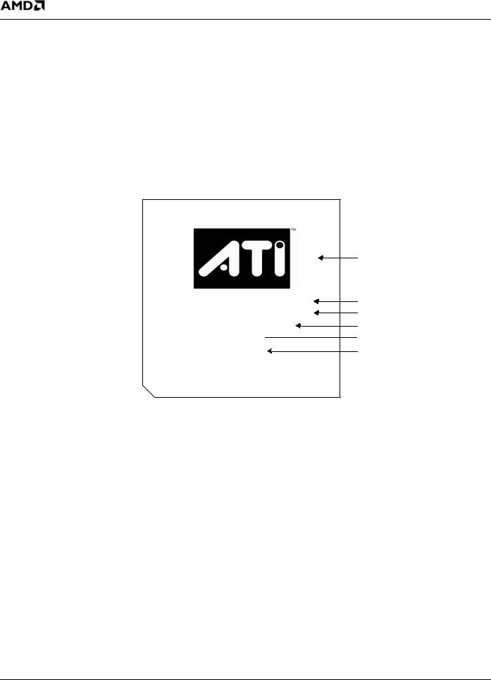
1.6Branding Diagrams
1.6.1Branding Diagram for ASIC Revision A11
RS690T
216TQA6AVA11FG GGGGG YYWWXXV  TAIWAN
o
Artwork
AMD Code Name
Part Number (for ASIC revision A11)
Wafer Foundry’s Lot Number
Date and Other Codes*
Country of Origin
*YY - Assembly Start Year
WW- Assembly Start Week
XX- Assembly Location
V - Substrate Vendor Code
Figure 1-1 M690T Branding Diagram for ASIC Revision A11
1.6.2Branding Diagram for ASIC Revision A12 and After
Note: The branding diagram below does not necessarily contain the latest ASCI revision number for the M690T. Unless specified otherwise, no information in this databook is specific to the ASIC revision number given in the diagram.
42437 AMD M690T/E Databook 3.10 |
© 2011 Advanced Micro Devices, Inc. |
1-8 |
Proprietary |
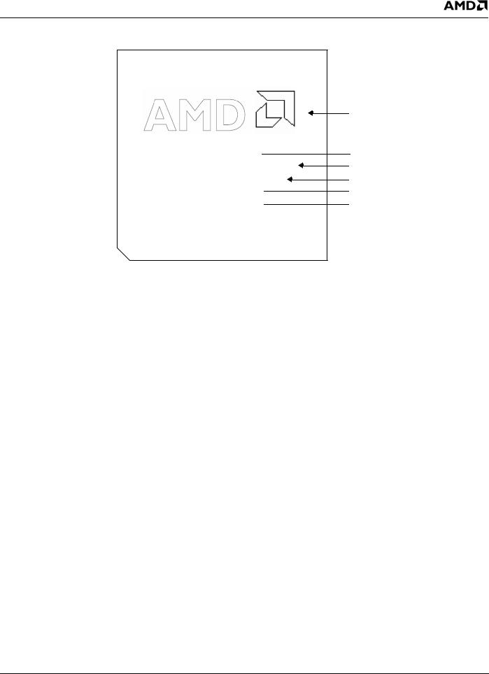
Branding Diagrams
CHIPSET  216TQA6AVA12FG GGGGGG YYWWXXV
  COO
COO 
o
AMD Logo
AMD Product Type
Part Number (for ASIC revision A12)
Wafer Foundry’s Lot Number
Date and Other Codes*
Country of Origin
*YY - Assembly Start Year
WW- Assembly Start Week
XX- Assembly Location
V - Substrate Vendor Code
“o” indicates pin A1.
Figure 1-2 M690T Branding Diagram for ASIC Revision A12
© 2011 Advanced Micro Devices, Inc. |
42437 AMD M690T/E Databook 3.10 |
Proprietary |
1-9 |
Part Number Legend
1.7Part Number Legend
Marketing
Brand Name
TQA6 - M690T
Foundry Code
N – UMC Fab 8F
M– IBM
C – TSMC Fab 3
S – TSMC Fab 4
F – TSMC Fab 5
G – TSMC Fab6
K – TSMC Fab 12
L – TSMC Fab14
W– TSMC WSMC
Q – TSMC WSMC(8B)
T – TSMC Wafer Tech
V – UMC Fab 12A
Flip Chip
Blank – No
F – Yes
216 TQA6 |
A |
V |
A12 |
F |
G |
Product Type |
|
Substrate |
|
ASIC |
|
Package BOM |
||
215– |
Desktop |
|
Revision |
|
Revision |
|
K– |
High Temp |
216– |
Mobile |
|
|
|
|
|
G – |
Lead Free |
Figure 1-3 M690T ASIC Part Number Legend
1.8Production Schedule, OPN, and Part Marking
The part marking, planned production schedule, and AMD OPN (ordering numbering) for the M690T are shown in
Table 1-2.
Table 1-2 M690T Planned production Schedule, OPN, and Part Marking
Component |
Production Availability Date |
OPN |
Part Marking |
M690T |
In production now |
100-CG1292 |
216TQA6AVA12FG |
|
|
|
|
1.9Conventions and Notations
The following conventions are used throughout this manual.
1.9.1Pin Names
Pins are identified by their pin names or ball references. Multiplexed pins assume alternate “functional names” when they perform their alternate functions, and these “functional names” are given in Chapter 3, “Pin Descriptions and Strap Options.”
All active-low signals are identified by the suffix ‘#’ in their names (e.g., LDTSTOP#).
1.9.2Pin Types
The pins are assigned different codes according to their operational characteristics. These codes are listed in Table 1-3.
42437 AMD M690T/E Databook 3.10 |
© 2011 Advanced Micro Devices, Inc. |
1-10 |
Proprietary |
Conventions and Notations
Table 1-3 Pin Type Codes
Code |
Pin Type |
I |
Digital Input |
|
|
O |
Digital Output |
|
|
OD |
Open Drain |
|
|
I/O |
Bi-Directional Digital Input or Output |
|
|
M |
Multifunctional |
|
|
Pwr |
Power |
|
|
Gnd |
Ground |
|
|
A-O |
Analog Output |
|
|
A-I |
Analog Input |
|
|
A-I/O |
Analog Bi-Directional Input/Output |
|
|
A-Pwr |
Analog Power |
|
|
A-Gnd |
Analog Ground |
|
|
Other |
Pin types not included in any of the categories above |
|
|
1.9.3Numeric Representation
Hexadecimal numbers are appended with “h” (Intel assembly-style notation) whenever there is a risk of ambiguity. Other numbers are in decimal.
Pins of identical functions but different trailing integers (e.g., “CPU_D0, CPU_D1,... CPU_D7”) are referred to collectively by specifying their integers in square brackets and with colons (i.e., “CPU_D[7:0]”). A similar short-hand notation is used to indicate bit occupation in a register. For example, NB_COMMAND[15:10] refers to the bit positions 10 through 15 of the NB_COMMAND register.
1.9.4Register Field
A field of a register is referred to by the format of [Register Name].[Register.Field]. For example, “NB_MC_CNTL.DISABLE_BYPASS” is the “DISABLE_BYPASS” field of the register “NB_MC_CNTL.”
1.9.5Hyperlinks
Phrases or sentences in blue italic font are hyperlinks to other parts of the manual. Users of the PDF version of this manual can click on the links to go directly to the referenced sections, tables, or figures.
1.9.6Acronyms and Abbreviations
The following is a list of the acronyms and abbreviations used in this manual.
Table 1-4 Acronyms and Abbreviations
Acronym |
Full Expression |
|
ACPI |
Advanced Configuration and Power Interface |
|
|
|
|
A-Link-E II |
A-Link Express II interface between the IGP and the Southbridge. |
|
|
|
|
BGA |
Ball Grid Array |
|
|
|
|
BIOS |
Basic Input Output System. Initialization code stored in a ROM or Flash RAM used to start up a |
|
system or expansion card. |
||
|
||
|
|
|
BIST |
Built In Self Test. |
|
|
|
|
BLT |
Blit |
|
|
|
|
bpp |
bits per pixel |
|
|
|
|
CEC |
Consumer Electronic Control |
|
|
|
|
CPIS |
Common Panel Interface Specification |
|
|
|
|
CRT |
Cathode Ray Tube |
|
|
|
|
CSP |
Chip Scale Package |
|
|
|
© 2011 Advanced Micro Devices, Inc. |
42437 AMD M690T/E Databook 3.10 |
Proprietary |
1-11 |

Conventions and Notations
Table 1-4 Acronyms and Abbreviations (Continued)
Acronym |
Full Expression |
|
DAC |
Digital to Analog Converter |
|
|
|
|
DBI |
Dynamic Bus Inversion |
|
|
|
|
DDC |
Display Data Channel. A VESA standard for communicating between a computer system and |
|
attached display devices. |
||
|
||
|
|
|
DDR |
Double Data Rate |
|
|
|
|
DFP |
Digital Flat Panel. Monitor connection standard from VESA. |
|
|
|
|
DPM |
Defects per Million |
|
|
|
|
DTV |
Digital TV |
|
|
|
|
DVD |
Digital Video Disc |
|
|
|
|
DVI |
Digital Video Interface. Monitor connection standard from the DDWG (Digital Display Work |
|
Group). |
||
|
||
|
|
|
DVS |
Digital Video Stream |
|
|
|
|
EPROM |
Erasable Programmable Read Only Memory |
|
|
|
|
FIFO |
First In, First Out |
|
|
|
|
FPDI |
Flat Panel Display Interface |
|
|
|
|
GDI |
Graphics Device Interface |
|
|
|
|
GND |
Ground |
|
|
|
|
GPIO |
General Purpose Input/Output |
|
|
|
|
GTL+ |
Gunning Transceiver Logic |
|
|
|
|
HDCP |
High-Bandwidth Digital Content Protection |
|
|
|
|
HDMI |
High Definition Multimedia Interface |
|
|
|
|
HDTV |
High Definition TV. The 1920x1080 and the 1280x720 modes defined by ATSC. |
|
|
|
|
HPD |
Hot Plug Detect |
|
|
|
|
iDCT |
inverse Discrete Cosine Transform |
|
|
|
|
IDDQ |
Direct Drain Quiescent Current |
|
|
|
|
IGP |
Integrated Graphics Processor. A single device that integrates a graphics processor and a |
|
system controller. |
||
|
||
|
|
|
JTAG |
Joint Test Access Group. An IEEE standard. |
|
|
|
|
LVDS |
Low Voltage Differential Signaling |
|
|
|
|
MB |
Mega Byte |
|
|
|
|
MPEG |
Motion Pictures Experts Group. Refers to compressed video image streams in either MPEG-1 |
|
or MPEG-2 formats. |
||
|
||
|
|
|
NTSC |
National Television Standards Committee. The standard definition TV system used in North |
|
America and other areas. |
||
|
||
|
|
|
PAL |
Phase Alternate Line. The standard definition TV system used in Europe and other areas. |
|
|
|
|
PCI |
Peripheral Component Interface |
|
|
|
|
PCIe |
PCI Express |
|
|
|
|
PCMCIA |
Personal Computer Memory Card International Association. It is also the name of a standard |
|
for PC peripherals promoted by the Association. |
||
|
||
|
|
|
PLL |
Phase Locked Loop |
|
|
|
|
POST |
Power On Self Test |
|
|
|
|
PD |
Pull-down Resistor |
|
|
|
|
PU |
Pull-up Resistor |
|
|
|
|
ROP |
Raster Operation |
|
|
|
|
SDRAM |
Synchronous Dynamic RAM |
|
|
|
|
TMDS |
Transition Minimized Differential Signaling |
|
|
|
|
UMA |
Unified Memory Architecture |
|
|
|
|
UV |
Chrominance (also CrCb). Corresponds to the color of a pixel. |
|
|
|
|
UXGA |
Ultra Extended Graphics Array |
|
|
|
|
VBI |
Vertical Blank Interval |
|
|
|
|
VESA |
Video Electronics Standards Association |
|
|
|
42437 AMD M690T/E Databook 3.10 |
© 2011 Advanced Micro Devices, Inc. |
1-12 |
Proprietary |

Conventions and Notations
Table 1-4 Acronyms and Abbreviations (Continued)
Acronym |
Full Expression |
VGA |
Video Graphics Adapter |
|
|
VRM |
Voltage Regulation Module |
|
|
© 2011 Advanced Micro Devices, Inc. |
42437 AMD M690T/E Databook 3.10 |
Proprietary |
1-13 |

Conventions and Notations
This page is left blank intentionally.
42437 AMD M690T/E Databook 3.10 |
© 2011 Advanced Micro Devices, Inc. |
1-14 |
Proprietary |
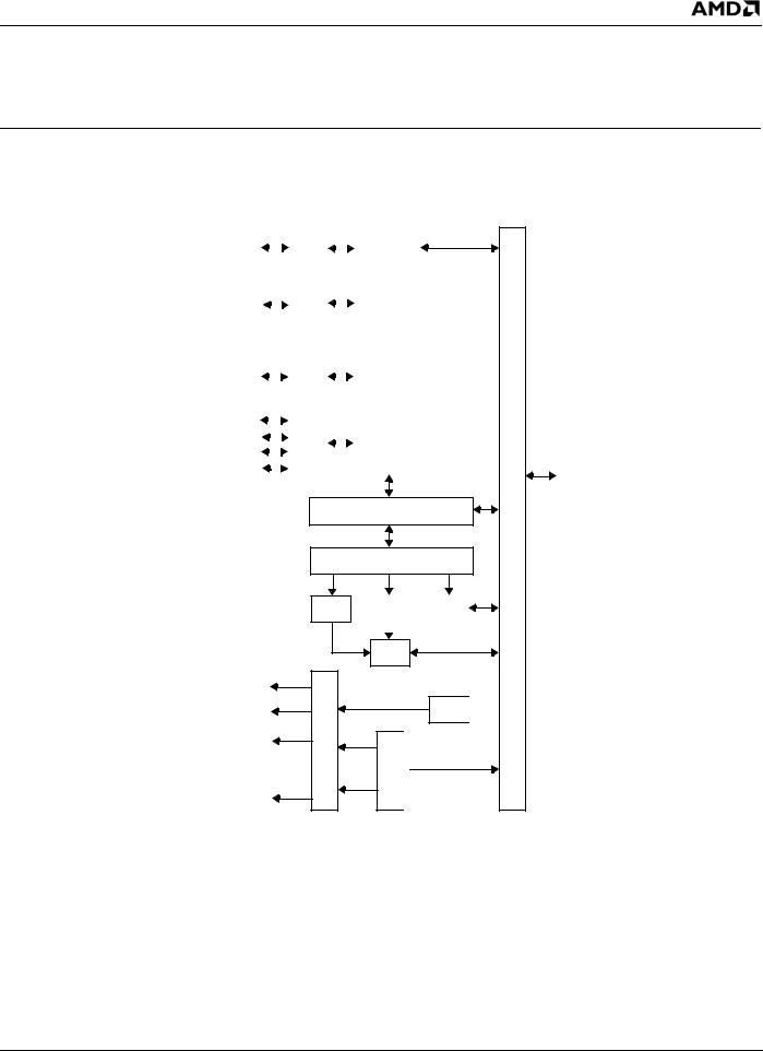
Chapter 2
Functional Descriptions
This chapter describes the functional operation of the major interfaces of the M690T system logic chip. Figure 2-1, “M690T Internal Block Diagram,” illustrates the M690T internal blocks and interfaces.
|
|
|
|
|
|
|
|
|
|
|
Interface |
|
|
|
HyperTransport™ |
|
|
|
|
|
|
|
|
|
|
|
|
|
CPU |
|
|
|
|
AMD CPU |
|
|
|
|
|
|
|
|
|
|
|
|
|
Unit |
||
|
|
|
|
|
|
|
|
|
|
|
|
|
|
|||
|
|
|
|
|
|
|
|
|
|
|
|
|
|
|
||
|
|
|
|
|
|
|
|
|
|
|
|
|
|
|
|
|
SB |
|
|
|
|
|
IIE-Link-A Interface Lanes)4 x (1 |
|
|
|
|
||||||
|
|
|
|
|
|
|
|
|
|
|
||||||
|
|
|
|
|
|
|
|
|
||||||||
|
|
|
|
|
|
|
|
|
|
|
|
|
|
|
|
|
|
|
|
|
|
|
|
|
|
|
|
|
|
|
|
|
|
|
|
|
|
|
|
|
|
|
|
Interface Gfx Lanes) 8 x (1 |
|
|
|
|
Root |
|
External |
PCIe |
|
|
|
Complex |
|||||||||||
|
|
|
|
|||||||||||||
Graphics |
|
|
|
|
|
|
|
|
|
|
||||||
|
|
|
|
|
|
|
|
|
|
|||||||
|
|
|
|
|
|
|
|
|
|
® |
|
|
|
|
||
|
|
|
|
|
|
|
|
|
|
|
|
|
|
|
||
|
|
|
|
|
|
|
|
|
|
|
||||||
Expansion |
|
|
|
|
Lanes)1 x (4 |
InterfaceGPP |
PCIe |
|
|
|
|
|||||
|
|
|
|
|
|
|
||||||||||
Slots or |
|
|
|
|
|
|
|
|||||||||
|
|
|
|
|
|
|||||||||||
On-board |
|
|
|
|
|
|
|
|
||||||||
Devices |
® |
|
|
|
|
|||||||||||
|
|
|
|
|
|
|
|
|
|
|
|
|
|
|
|
|
|
|
|
|
|
|
|
|
|
|
|
|
|
|
|
|
|
BIF
Register Interface
TMDS, enabling DVI/HDM™I (Multiplexed on PCIe® Gfx lanes)
External Display via DVO
TV-Out
LVDS 
CRT
iDCT
MUX
Setup |
|
2D |
|
Engine |
|
Engine |
|
|
|
|
|
3D Engine
Overlay

 2 1& Display
Controller Memory
Optional 16-bit DDR2
Memory Channel
Figure 2-1 M690T Internal Block Diagram
© 2011 Advanced Micro Devices, Inc. |
42437 AMD M690T/E Databook 3.10 |
Proprietary |
2-1 |
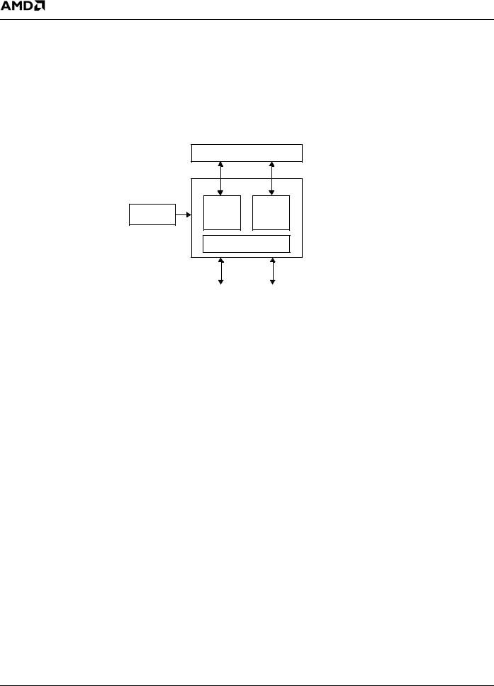
Host Interface
2.1Host Interface
The M690T is designed to interface with the AMD Athlon 64/AMD Athlon 64 FX/AMD Athlon X2/AMD Sempron/AMD Turion 64 processors, including both AM2 and S1 socket CPUs. This section presents an overview of the HyperTransport™ interface. For a detailed description of the interface, please refer to the HyperTransport I/O Link Specification from the HyperTransport Consortium. Figure 2-2, “Host Interface Block Diagram,” illustrates the basic blocks of the host bus interface of the M690T.
|
HT Interface to CPU (PHY) |
|
Configuration |
LTA |
LRA |
Registers |
|
|
|
|
SCH |
Data Link Layer
Protocol/Transaction Layer
Root Complex |
|
Memory Controller |
|
|
|
Figure 2-2 Host Interface Block Diagram
The HyperTransport (HT) Interface is a high speed, packet-based link implemented on two unidirectional buses. It is a point-to-point interface where data can flow both upstream and downstream at the same time. The commands, addresses, and data travel in packets on the HyperTransport link. Lengths of packets are in multiples of four bytes. The HT link consists of three parts: the physical layer (PHY), the data link layer, and the protocol/transaction layer. The PHY is the physical interface between the M690T and the CPU. The data link layer includes the initialization and configuration sequences, periodic redundancy checks, connect/disconnect sequences, and information packet flow controls. The protocol layer is responsible for maintaining strict ordering rules defined by the HT protocol.
The M690T HyperTransport bus interface consists of 17 unidirectional differential data/control pairs and two differential clock pairs in each of the upstream and downstream direction. On power up, the HT link is 8 bits wide and runs at a default speed of 200MT/s. After negotiation, carried out by the HW and SW together, the link width can be brought up to 16 bits and the interface can run up to 2GT/s. The interface is illustrated in Figure 2-3, “M690T Host Bus Interface Signals,” on page 2-3. The signal name and direction for each signal is shown with respect to the processor. Please note that the signal names may be different from those used in the pin listing of the M690T. Detailed descriptions of the signals are given in section 3.3, “CPU HyperTransport™ Interface‚’ on page 3-5.
42437 AMD M690T/E Databook 3.10 |
© 2011 Advanced Micro Devices, Inc. |
2-2 |
Proprietary |
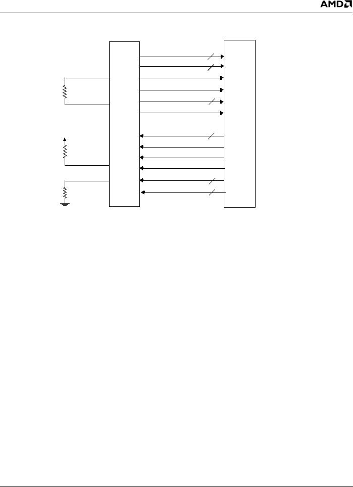
Side-port Memory Interface
HT_TXCALN
HT_TXCALP
M690T
VDD_HT
HT_RXCALN
HT_RXCALP
HT_TXCLKP 2
HT_TXCLKN 2
HT_TXCTLP
HT_TXCTLN
HT_TXCADP 16
HT_TXCADN 16
HT_RXCLKP 2
HT_RXCLKN 2
HT_RXCTLP
HT_RXCTLN
HT_RXCADP 16
HT_RXCADN 16
CPU AMD
Figure 2-3 M690T Host Bus Interface Signals
2.2Side-port Memory Interface
In order to significantly decrease system power and increase graphics performance, the M690T provides an optional side-port memory interface for dedicated frame buffer memory, to be used exclusively for the integrated graphics core. The side-port memory interface is designed to significantly reduce system power by allowing the CPU to stay in its lowest power state during periods of inactivity. Screen refreshes are fetched from the side-port memory, and there is no need to "wake up" the CPU to fetch screen refresh data.
The M690T memory controller operates in 16-bit mode at very high speed (up to DDR2-800), and has a new programmable interleaved mode that significantly increases the memory bandwidth and reduces data latency to the integrated graphics core.
2.2.1DDR2 Memory Interface
Figure 2-4, “M690T Side-port Memory Interface,” on page 2-4, illustrates the side-port memory interface of the M690T.
The M690T memory controller supports up to 128MB of dedicated side-port frame buffer memory. It controls a single rank of DDR2 devices in 16-bit memory configuration. It supports device sizes of 256, 512, and 1024 Mbit, and device widths of x8 and x16. Because the memory controller supplies only one chip select signal, only DDR2 devices with one chip select are supported. A wide range of DDR2 timing parameters, configurations, and loadings are programmable via the M690T memory controller configuration registers
© 2011 Advanced Micro Devices, Inc. |
42437 AMD M690T/E Databook 3.10 |
Proprietary |
2-3 |
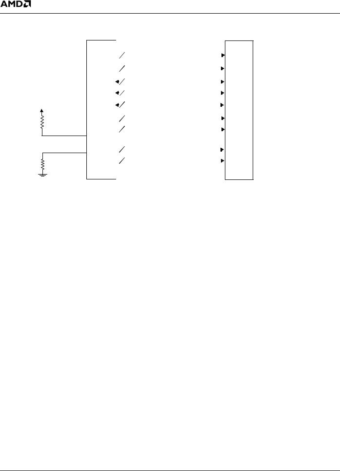
Side-port Memory Interface
VDD_MEM
MEM_CALN
MEM_CALP
Interface
|
|
|
14 |
Address MEM_A[13:0] |
||
|
|
|
3 |
Bank Address MEM_BA[2:0] |
||
M690T |
16 |
Data MEM_DQ[15:0] |
||||
|
|
|
||||
|
4 |
Data Strobes MEM_DQS[1:0]P/N |
||||
|
|
|
||||
-Side |
2 |
Data Mask MEM_DM[1:0] |
||||
|
2 Differential Clocks MEM_CKP/MEM_CKN |
|||||
port |
|
|
|
|||
|
1 |
Chip Select MEM_CS# |
||||
Memory |
|
|
|
|||
|
|
MEM_CKE, MEM_RAS#, |
||||
|
|
|
4 |
MEM_CAS#, MEM_WE# |
||
|
|
|
|
|
||
|
|
|
1 |
On-Die Termination MEM_ODT |
||
|
|
|
|
|
|
|
SDRAM DDR2 buffered-Un
Figure 2-4 M690T Side-port Memory Interface
2.2.1.1 Supported DDR2 Components
The memory controller supports DDR2 SDRAM chips in several configurations. These chips are organized in banks, rows (or pages), and columns. The supported DDR2 components have four or eight banks. Table 2-1 lists the supported memory components.
Table 2-1 Supported DDR2 Components |
|
|
|
||||
|
|
|
|
|
|
|
|
|
|
DDR2 SDRAM |
|
|
Mbytes |
||
Config |
Mbits |
CS Mode |
Bank Bits |
Row Bits |
Col Bits |
||
|
|||||||
16Mbits x 16 |
256 |
4 |
2 |
13 |
9 |
32 |
|
|
|
|
|
|
|
|
|
32Mbits x 8 |
256 |
5 |
2 |
13 |
10 |
64 |
|
|
|
|
|
|
|
|
|
32Mbits x 16 |
512 |
10 |
2 |
13 |
10 |
64 |
|
|
|
|
|
|
|
|
|
64Mbits x 8 |
512 |
6 |
2 |
14 |
10 |
128 |
|
|
|
|
|
|
|
|
|
64Mbits x 16 |
1024 |
11 |
3 |
13 |
10 |
128 |
|
|
|
|
|
|
|
|
|
2.2.1.2 Row and Column Addressing
Table 2-2 shows how the physical address P (after taking out the bank bit) is used to provide the row and column addressing for each size of DDR2 memories.
Table 2-2 DDR2 Memory Row and Column Addressing
|
|
|
|
|
|
|
Address |
|
|
|
|
|
|
||
|
A13 |
A12 |
A11 |
A10 |
A9 |
A8 |
A7 |
A6 |
A5 |
A4 |
A3 |
A2 |
A1 |
A0 |
|
|
|
|
|
|
|
16Mbits x16 devices |
|
|
|
|
|
|
|||
Row |
|
P10 |
P14 |
P13 |
P12 |
P11 |
P22 |
P21 |
|
P20 |
P19 |
P18 |
P17 |
P16 |
P15 |
Column |
|
- |
- |
PC |
- |
P9 |
P8 |
P7 |
|
P6 |
P5 |
P4 |
P3 |
P2 |
P1 |
|
|
|
|
|
|
32Mbits x8 devices |
|
|
|
|
|
|
|||
Row |
|
P23 |
P14 |
P13 |
P12 |
P11 |
P22 |
P21 |
|
P20 |
P19 |
P18 |
P17 |
P16 |
P15 |
Column |
|
- |
- |
PC |
P10 |
P9 |
P8 |
P7 |
|
P6 |
P5 |
P4 |
P3 |
P2 |
P1 |
42437 AMD M690T/E Databook 3.10 |
© 2011 Advanced Micro Devices, Inc. |
2-4 |
Proprietary |

Side-port Memory Interface
|
|
|
|
|
|
|
|
Address |
|
|
|
|
|
|
|
||
|
A13 |
|
A12 |
A11 |
A10 |
A9 |
A8 |
A7 |
A6 |
A5 |
A4 |
A3 |
A2 |
|
A1 |
A0 |
|
|
|
|
|
|
|
|
32Mbits x16 devices |
|
|
|
|
|
|
|
|||
Row |
|
|
P23 |
P14 |
P13 |
P12 |
P11 |
P22 |
P21 |
|
P20 |
P19 |
P18 |
P17 |
|
P16 |
P15 |
Column |
|
- |
- |
PC |
P10 |
P9 |
P8 |
P7 |
|
P6 |
P5 |
P4 |
P3 |
|
P2 |
P1 |
|
|
|
|
|
|
|
|
64Mbits x8 devices |
|
|
|
|
|
|
|
|||
Row |
P24 |
|
P23 |
P14 |
P13 |
P12 |
P11 |
P22 |
P21 |
|
P20 |
P19 |
P18 |
P17 |
|
P16 |
P15 |
|
|
|
|
|
|
|
|
|
|
|
|
|
|
|
|
|
|
Column |
|
|
- |
- |
PC |
P10 |
P9 |
P8 |
P7 |
|
P6 |
P5 |
P4 |
P3 |
|
P2 |
P1 |
|
|
|
|
|
|
|
|
|
|
|
|
|
|
|
|
|
|
|
|
|
|
|
|
|
64Mbits x16 devices |
|
|
|
|
|
|
|
|||
Row |
|
|
P23 |
P14 |
P13 |
P12 |
P11 |
P22 |
P21 |
|
P20 |
P19 |
P18 |
P17 |
|
P16 |
P15 |
|
|
|
|
|
|
|
|
|
|
|
|
|
|
|
|
|
|
Column |
|
|
- |
- |
PC |
P10 |
P9 |
P8 |
P7 |
|
P6 |
P5 |
P4 |
P3 |
|
P2 |
P1 |
|
|
|
|
|
|
|
|
|
|
|
|
|
|
|
|
|
|
Note: PC = precharge flag |
|
|
|
|
|
|
|
|
|
|
|
|
|
||||
© 2011 Advanced Micro Devices, Inc. |
42437 AMD M690T/E Databook 3.10 |
Proprietary |
2-5 |

LVDS Interface
2.3LVDS Interface
The M690T contains a dual-channel 24-bit LVDS interface. Notice that for designs implementing only a single LVDS channel, the LOWER channel of the interface should be used.
2.3.1 LVDS Data Mapping
Figure 2-5 below shows the transmission ordering of the LVDS signals on the lower and the upper data channels. The signal mappings for single and dual channel transmission are shown in Table 2-3 and Table 2-4 respectively.
T Cycle
TXCLK_L-/+
TXOUT_L0-/+
TXOUT_L1-/+
TXOUT_L2-/+
TXOUT_L3-/+
TXCLK_U-/+
LP1C7  LP1C6
LP1C6  LP1C5
LP1C5  LP1C4
LP1C4  LP1C3
LP1C3  LP1C2
LP1C2  LP1C1
LP1C1
LP2C7  LP2C6
LP2C6  LP2C5
LP2C5  LP2C4
LP2C4  LP2C3
LP2C3  LP2C2
LP2C2  LP2C1
LP2C1
LP3C7  LP3C6
LP3C6  LP3C5
LP3C5  LP3C4
LP3C4  LP3C3
LP3C3  LP3C2
LP3C2  LP3C1
LP3C1
LP4C7  LP4C6
LP4C6  LP4C5
LP4C5  LP4C4
LP4C4  LP4C3
LP4C3  LP4C2
LP4C2  LP4C1
LP4C1
T Cycle
TXOUT_U0-/+
TXOUT_U1-/+
TXOUT_U2-/+
TXOUT_U3-/+
UP1C7  UP1C6
UP1C6  UP1C5
UP1C5  UP1C4
UP1C4  UP1C3
UP1C3  UP1C2
UP1C2  UP1C1
UP1C1
UP2C7  UP2C6
UP2C6  UP2C5
UP2C5  UP2C4
UP2C4  UP2C3
UP2C3  UP2C2
UP2C2  UP2C1
UP2C1
UP3C7  UP3C6
UP3C6  UP3C5
UP3C5  UP3C4
UP3C4  UP3C3
UP3C3  UP3C2
UP3C2  UP3C1
UP3C1
UP4C7  UP4C6
UP4C6  UP4C5
UP4C5  UP4C4
UP4C4  UP4C3
UP4C3  UP4C2
UP4C2  UP4C1
UP4C1
Figure 2-5 Single/Dual Channel 24-bit LVDS Data Transmission Ordering
42437 AMD M690T/E Databook 3.10 |
© 2011 Advanced Micro Devices, Inc. |
2-6 |
Proprietary |
Loading...