


 Loading...
& K D S W H U
System Board
The V55LA-2 is a high-performance system board with a 64-bit architecture. It supports the Intel P54C and P55C CPUs running at 75/90/100/120/133/150/166/200 MHz. It also supports Cyrix M1/M2 and AMD K5/K6 CPUs. The system board utilizes the Peripheral Component Interconnect (PCI) local bus architecture that maximizes the system performance by enabling high-speed peripherals to match the speed of the microprocessor with its 120 MB or 132 MB per second transfer rate in burst mode.
The board incorporates a Sound Blaster Pro-compatible audio subsystem that consists of CD-audio, WaveTable, and fax/modem line-in interfaces.
A standard 1-MB video DRAM comes onboard and is upgradable up to 2 MB. Two DRAM banks composed of four 72-pin sockets come with the board to support singleand double-density SIMMs for a maximum system memory of 128 MB. The SIMM sockets accommodate both the standard page mode and extended data output (EDO) type SIMMs. The board supports 256-KB or 512-KB pipeline burst secondlevel cache.
The system board includes a 188-pin connector for the slot board that contains the PCI and ISA bus slots. The two onboard PCI-enhanced IDE interfaces with a zero-wait state and 16.6 MB per second transfer rate support up to four IDE devices. Onboard I/O interfaces comprise of two UART 16550 serial ports, a parallel port with ECP/EPP feature, and PS/2 keyboard and mouse ports.
System Board |
1-1 |

1.1Major Features
The system board has the following major features:
∙A zero-insertion force (ZIF) socket for Intel P54C and P55C, Cyrix M1/M2, or AMD K5/K6
∙Two DRAM banks composed of four 72-pin SIMM sockets that support 4/8/16/32-MB 60/70ns SIMMs
∙256-KB or 512-KB write-back pipeline burst second-level cache (manufacturing option)
∙256-KB boot block mode Flash ROM for system BIOS, VGA BIOS, and PnP ESCD
∙Two PCI-enhanced IDE interfaces that support up to four IDE devices
∙System clock/calendar with 256-byte CMOS RAM
∙Interfaces for CD-audio, fax/voice modem, and WaveTable support
∙Standard 1-MB video DRAM onboard plus two upgrade sockets for up to 2-MB video memory
∙188-pin connector for PCI/ISA slot board
∙Feature socket for multimedia or Ethernet solution
∙External ports:
∙PS/2 keyboard and mouse ports
∙Two buffered high-speed serial ports
∙One ECP/EPP high-speed parallel port
∙Video port
1-2 |
User’s Guide |
1.1.1System Board
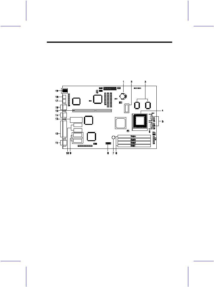
Figure 1-1 shows the locations of the system board major components.
1 |
Battery |
11 |
Video port |
2 |
Tag SRAM |
12 |
Parallel port |
3 |
Pipeline burst second-level cache |
13 |
BIOS |
4 |
Pentium CPU socket |
14 |
Serial port 2 |
5 |
CPU voltage regulators |
15 |
Slot board connector |
6 |
SIMM sockets |
16 |
Serial port 1 |
7 |
Buzzer |
17 |
Mouse port |
8 |
Switch 2 (SW2) |
18 |
Keyboard port |
9 |
Video RAM upgrade sockets |
19 |
USB connector |
10 |
Video RAM |
|
|
Figure 1-1 System Board Layout
System Board |
1-3 |
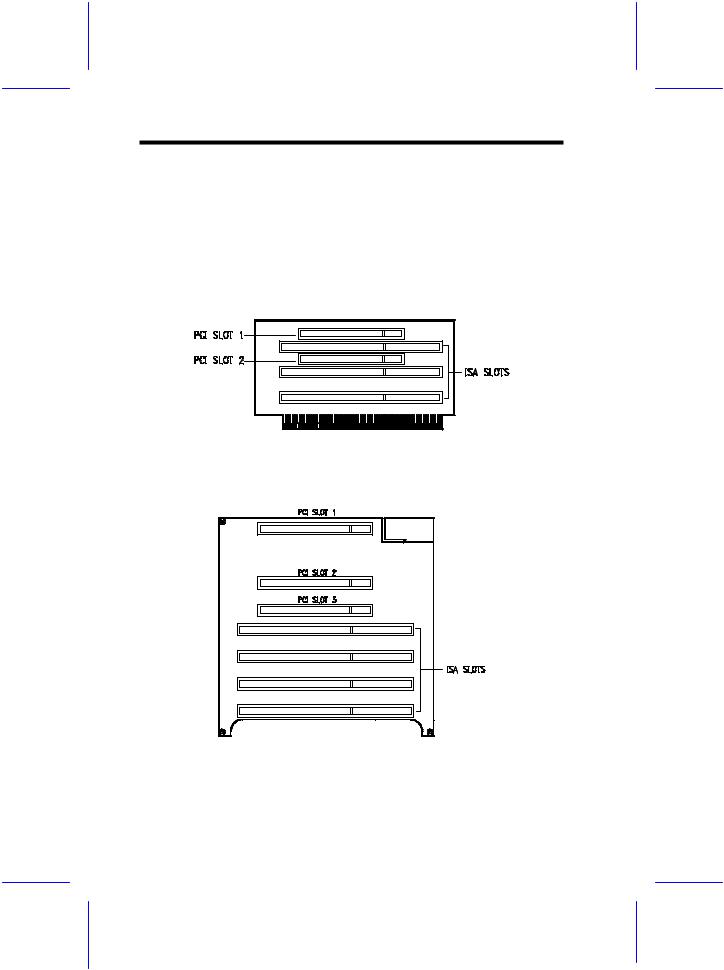
1.1.2Slot Boards
The system board comes with a slot board already installed. The slot board carries the PCI and ISA bus slots for system enhancements and future expansion.
The slot board may vary in size and layout depending on your system housing. Figures 1-2 and 1-3 show the two kinds of slot boards.
Figure 1-2 2-PCI/3-ISA Slot Board (for Aspire desktop systems)
Figure 1-3 3-PCI/4-ISA Slot Board
(for Aspire minitower systems)
1-4 |
User’s Guide |

1.2Jumpers and Connectors
1.2.1Jumper and Connector Locations
Figure 1-4 shows the jumper and connector locations on the system board.
Figure 1-4 System Board Jumper and Connector Locations
The blackened pin of a jumper represents pin 1.
System Board |
1-5 |

1.2.2Jumper Settings
Table 1-1 lists the system board jumpers with their corresponding settings and functions.
Table 1-1 |
System Board Jumper Settings |
||
|
|
|
|
Jumper |
|
Setting |
Function |
BIOS Type |
|
|
|
JP1 |
|
1-2 |
For models with Acer BIOS |
|
|
2-3 |
For models with OEM BIOS |
|
|
|
|
LED Function |
|
|
|
JP2 |
|
1-2 |
LED for IDE and FDD |
|
|
2-3 |
LED for IDE only |
|
|
|
|
Second-level Cache |
|
|
|
JP3, JP4 |
|
1-2, 1-2 |
256 KB |
|
|
1-2, 2-3 |
512 KB |
|
|
2-3, 2-3 |
1 MB |
|
|
|
|
Regulator |
|
|
|
JP7 |
|
Closed |
For single-voltage CPUs (P54C, K5, M1) |
|
|
Open |
For dual-voltage CPUs (P55C, K6, M2) |
|
|
|
|
SMM/Reset Switch |
|
|
|
JP11 |
|
1-2 |
CN19 pins 19-20 support SMM switch |
|
|
2-3 |
Reserved |
|
|
|
|
Software Shutdown |
|
|
|
JP16 |
|
1-2 |
UPS enabled |
|
|
2-3 |
UPS disabled |
|
|
|
|
CPU Voltage |
|
|
|
JP43 (for I/O) |
1-2 |
3.5V |
|
|
|
2-3 |
3.3V |
JP44 (for core) |
1-2 |
3.2V |
|
|
|
2-3 |
2.8V |
|
|
|
|
1-6 |
User’s Guide |

Tables 1-2 to 1-4 show the settings of DIP switch 2 (SW2), JP7, JP43, and JP44 for CPU selection.
Table 1-2 SW2, JP7, JP43, and JP44 Settings
CPU Freq. |
Host Bus |
|
|
|
|
|
|
|
(MHz) |
Freq. (MHz) |
SW1 SW2 SW3 SW4 |
JP7 |
JP43 |
JP44 |
|||
Intel P54C |
|
|
|
|
|
|
|
|
P75 |
50 |
On |
On |
Off |
Off |
Closed |
2-3 |
2-3 |
|
|
|
|
|
|
|
|
|
P90 |
60 |
On |
Off |
Off |
Off |
Closed |
2-3 |
2-3 |
|
|
|
|
|
|
|
|
|
P100 |
66 |
Off |
On |
Off |
Off |
Closed |
2-3 |
2-3 |
|
|
|
|
|
|
|
|
|
P120 |
60 |
On |
Off |
On |
Off |
Closed |
2-3 |
2-3 |
|
|
|
|
|
|
|
|
|
P133 |
66 |
Off |
On |
On |
Off |
Closed |
2-3 |
2-3 |
|
|
|
|
|
|
|
|
|
P150 |
60 |
On |
Off |
On |
On |
Closed |
2-3 |
2-3 |
|
|
|
|
|
|
|
|
|
P166 |
66 |
Off |
On |
On |
On |
Closed |
2-3 |
2-3 |
|
|
|
|
|
|
|
|
|
P200 |
66 |
Off |
On |
Off |
On |
Closed |
2-3 |
2-3 |
|
|
|
|
|
|
|
|
|
Intel P55C |
|
|
|
|
|
|
|
|
P150 |
60 |
On |
Off |
On |
On |
Open |
2-3 |
2-3 |
|
|
|
|
|
|
|
|
|
P166 |
66 |
Off |
On |
On |
On |
Open |
2-3 |
2-3 |
|
|
|
|
|
|
|
|
|
P200 |
66 |
Off |
On |
Off |
On |
Open |
2-3 |
2-3 |
|
|
|
|
|
|
|
|
|
Cyrix M1 (6x86) |
|
|
|
|
|
|
|
|
P120+ |
50 |
On |
On |
On |
Off |
Closed |
2-3 |
2-3 |
|
|
|
|
|
|
|
|
|
P150+ |
60 |
On |
Off |
On |
Off |
Closed |
2-3 |
2-3 |
|
|
|
|
|
|
|
|
|
P166+ |
66 |
Off |
On |
On |
Off |
Closed |
2-3 |
2-3 |
|
|
|
|
|
|
|
|
|
Cyrix M1 (6x86L) |
|
|
|
|
|
|
|
|
P120+ |
50 |
On |
On |
On |
Off |
Open |
2-3 |
2-3 |
|
|
|
|
|
|
|
|
|
P150+ |
60 |
On |
Off |
On |
Off |
Open |
2-3 |
2-3 |
|
|
|
|
|
|
|
|
|
P166+ |
66 |
Off |
On |
On |
Off |
Open |
2-3 |
2-3 |
|
|
|
|
|
|
|
|
|
Cyrix M2 |
|
|
|
|
|
|
|
|
PR166 |
66 |
Off |
On |
On |
On |
Open |
2-3 |
2-3 |
|
|
|
|
|
|
|
|
|
PR180 |
60 |
On |
Off |
Off |
On |
Open |
2-3 |
2-3 |
|
|
|
|
|
|
|
|
|
PR200 |
66 |
Off |
On |
Off |
On |
Open |
2-3 |
2-3 |
|
|
|
|
|
|
|
|
|
System Board |
1-7 |

Table 1-2 SW2, JP7, JP43, and JP44 Settings (continued)
CPU Freq. |
Host Bus |
|
|
|
|
|
|
|
(MHz) |
Freq. (MHz) |
SW1 SW2 SW3 SW4 |
JP7 |
JP43 |
JP44 |
|||
AMD K5 |
|
|
|
|
|
|
|
|
PR75 |
50 |
On |
On |
Off |
Off |
Closed |
1-2 |
2-3 |
|
|
|
|
|
|
|
|
|
PR90 |
60 |
On |
Off |
Off |
Off |
Closed |
1-2 |
2-3 |
|
|
|
|
|
|
|
|
|
PR100 |
66 |
Off |
On |
Off |
Off |
Closed |
1-2 |
2-3 |
|
|
|
|
|
|
|
|
|
PR120 |
60 |
On |
Off |
On |
Off |
Closed |
1-2 |
2-3 |
|
|
|
|
|
|
|
|
|
PR133 |
66 |
Off |
On |
On |
Off |
Closed |
1-2 |
2-3 |
|
|
|
|
|
|
|
|
|
PR166 |
66 |
Off |
On |
On |
On |
Closed |
1-2 |
2-3 |
|
|
|
|
|
|
|
|
|
AMD K6 |
|
|
|
|
|
|
|
|
PR166 |
66 |
Off |
On |
On |
On |
Open |
2-3 |
1-2 |
|
|
|
|
|
|
|
|
|
PR200 |
66 |
Off |
On |
Off |
On |
Open |
2-3 |
1-2 |
|
|
|
|
|
|
|
|
|
PR233 |
66 |
Off |
On |
Off |
Off |
Open |
2-3 |
1-2 |
|
|
|
|
|
|
|
|
|
Table 1-3 |
SW2 Settings (Onboard Sound Chip) |
||
|
|
|
|
|
Setting 5 |
|
Function |
|
ON |
|
Onboard sound chip disabled |
|
|
|
|
|
OFF |
|
Onboard sound chip enabled |
|
|
|
|
Table 1-4 |
SW2 Settings (Password Security) |
||
|
|
|
|
|
Setting 6 |
|
Function |
|
ON |
|
Password bypass |
|
|
|
|
|
OFF |
|
Password check |
|
|
|
|
1-8 |
User’s Guide |

1.2.3Connector Functions
Table 1-5 lists the different connectors on the system board and their respective functions.
Table 1-5 Connector Functions
Connector |
Function |
CN1 |
Feature connector for multimedia or |
|
Ethernet solution |
|
|
CN2 |
CD-audio line-in connector |
|
|
CN3 |
Power connector |
|
|
CN5 |
USB connector |
|
|
CN6 |
WaveTable connector |
|
|
CN7 |
PS/2 keyboard connector |
|
|
CN8 |
PS/2 mouse connector |
|
|
CN9 |
Audio I/O board connector |
|
|
CN10 |
Diskette drive connector |
|
|
CN11 |
IDE connector 2 |
|
|
CN12 |
IDE connector 1 |
|
|
CN13 |
Serial port 1 |
|
|
CN14 |
Serial port 2 |
|
|
CN17 |
Parallel port |
|
|
CN18 |
CPU fan connector |
|
|
CN19 |
Multifunction connector |
|
|
CN21 |
Video port |
|
|
CN22 |
Fax/modem connector |
|
|
CN23 |
ATI multimedia connector |
|
|
System Board |
1-9 |

Table 1-5 Connector Functions (continued)
Connector |
Function |
CN31 |
Internal line-in connector |
|
|
JP48 |
Hard disk and message LED (pins 1-3-5) |
|
Power LED (pins 2-4-6) |
|
|
JP50 |
Power-on switch connector |
|
|
JP15 |
Standby power connector |
|
|
JP30 |
External battery connector |
|
|
See section 1.10.1 for details on power and LED cables to the connector JP48.
1.3ESD Precautions
Always observe the following electrostatic discharge (ESD) precautions before installing a system component:
1.Do not remove a component from its antistatic packaging until you are ready to install it.
2.Wear a wrist grounding strap before handling electronic components. Wrist grounding straps are available at most electronic component stores.
Do not attempt the procedures described in the following sections unless you are a qualified technician.
1-10 |
User’s Guide |
Loading...